Measuring the role of surface chemistry in silicon microphotonics
The silicon/silicon dioxide (Si/SiO2) interface plays a crucial role in the performance, cost, and reliability of most modern microelectronic devicesYablonovitch1 ; Chabal ; Fenner ; Yamashita ; Kobayashi ; Linnros ; Li ; Petitdidier , from the basic transistor to flash memory, digital cameras, and solar cells. Today the gate oxide thickness of modern transistors is roughly 5 atomic layers, with 8 metal wire layers required to transport all the signals within a microprocessor. In addition to the increasing latency of such reduced-dimension metal wires, further “Moore’s Law” scaling of transistor cost and density is predicted to saturate in the next decadeMuller2 . As a result, silicon-based microphotonics is being explored for the routing and generation of high-bandwidth signalsLiu ; Xu1 ; Boyraz ; Rong2 ; Notomi1 ; Notomi3 ; Song . In comparison to the extensive knowledge of the electronic properties of the Si/SiO2 interface, little is known about the optical properties of Si surfaces used in microphotonics. In this Letter, we explore the optical properties of the Si surface in the telecommunication-relevant wavelength band of - nm. Utilizing a high quality factor () optical microresonatorVahala1 to provide sensitivity down to a fractional surface optical loss of , we show that optical loss within Si microphotonic components can be dramatically altered by Si surface preparation, with measured for chemical oxide surfaces as compared to for hydrogen-terminated Si surfaces. These results indicate that the optical properties of Si surfaces can be significantly and reversibly altered by standard microelectronics treatments, and that stable, high optical quality surface passivation layers will be critical in future Si micro- and nano-photonic systems.
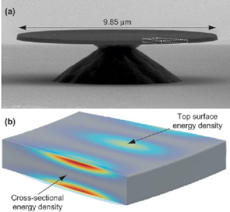
Historically, studies of Si surface and interface states have primarily focused on their electronic properties, with sensitive techniques such as deep-level transient spectroscopyLang1 or surface-sensitive minority carrier lifetime measurementsLinnros being employed. Three exceptions to this are deep-level optical spectroscopyChantre1 , cavity-ringdown spectroscopyAarts , and the ultra-sensitive technique of photothermal deflection spectroscopy (PDS)WB_Jackson1 ; Amato1 which can measure fractional optical absorption down to . None of the aforementioned techniques, however, is well suited for studying as-processed microphotonic elements. In this work we utilize a specially designed microdisk optical resonator to study the optical properties of surfaces typical in silicon-on-insulator (SOI) microphotonic elements in a noninvasive, rapid, and sensitive manner. Shown in Figure 1, the high quality factor () Si microdisk resonators used in this work provide surface-specific optical sensitivity due to the strong overlap of the top and bottom surfaces of the active Si layer with the electric field energy density of appropriately polarized bound optical modes of the microdisk. In addition, light within these micron-scale structures circulates tens of thousands of times, providing an effective path length approaching one meter.
A normalized measure of surface sensitivity for a guided-wave mode in a waveguide or resonator can be defined as , where is the fractional electric field energy overlap with a surface perturbation of physical depth . If optical loss is dominated by interactions with the surface, then the modal loss coefficient per unit length () measured from experiment can be related to a fractional loss per pass through the surface given by . As discussed in Ref. Blood1 , for a true two-dimensional surface in which the perturbation depth is infinitesimal, is the most relevant quantity describing the surface and is equivalent to the fraction of power lost for a normal incident plane wave propagating across the surface. is an important property of all surfaces in optics, yet it has historically rarely been measuredAmato1 , and is unknown today even for many important surfaces such as the -Si surfaces studied here. From finite-element method (FEM) simulationsSpillane3 , shown in Figure 1, the transverse magnetic (TM) polarization whispering-gallery-modes (WGMs) of the microdisk are more sensitive to the top and bottom Si surfaces than the etched sidewall at the microdisk periphery; specifically, nm-1 and nm-1. This implies that of the optical mode exists in a single monolayer at the top (bottom) Si surface, while little of the mode sees imperfections at the microdisk perimeter. At this level of sensitivity, a WGM with a (similar to the values measured in devices described below) can be used to measure fractional loss through the Si surface as small as . Such high- resonators can also be used to measure dispersive effectsTeraoka of the Si surface chemistry with a sensitivity corresponding to of a Si monolayer, or roughly Si atoms for a m radius microdisk.
The silicon microdisks studied in this work were fabricated from an SOI wafer commercially available from SOITEC, consisting of a nm thick silicon device layer (-type, cm resistivity, orientation) with a m SiO2 buried oxide (BOX) layer. Microdisks of and m radius were fabricatedBorselli2 , finishing with a minute acetone soak and Piranha etch to remove organic materials. A hour dilute hydrofluoric acid (HF) solution comprised of five parts M deionized (DI) water to one part concentrated aqueous HF (%) was used to remove a protective SiNx cap and partially undercut the disk, as shown in the SEM micrograph in Figure 1(a). The wafer was then rinsed in deionized water, dried with nitrogen (N2), and immediately transferred into an N2 purged testing enclosure.
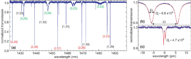
The microdisk resonators were characterized using a tunable external-cavity laser (- nm, linewidth MHz) connected to a computer-controlled fiber taper waveguide probeBorselli1 . The micron-scale fiber taper probe was formed from a standard single-mode optical fiber and was used to evanescently excite the WGMs of the microdisk with controllable loading. Figure 2 shows the normalized spectral transmission response of a 5 m radius microdisk resonator, illustrating clear families of modes having similar linewidth, , and free-spectral-range (FSR). By comparison to FEM simulations of the Si microdisk, each mode in Figure 2 was categorized and labelled as TMp,m, where and are the radial and azimuthal number, respectively.
Owing to their large surface sensitivity (see Figure 1), the spectral signature of the TM1,m modes was used to determine the quality of the optical surfaces. Figure 2(b) shows a high resolution scan across the TM1,31 mode. The observed double resonance dip, termed a doublet, is a result of surface roughness coupling of the normally degenerate clockwise (CW) and counter-clockwise (CCW) propagating WGMsGorodetsky ; Borselli2 ; Little2 . The rate at which photons are back-scattered is quantified by the doublet splitting, , while the rate at which photons are lost from the resonator is quantified by the intrinsic linewidth, , of the individual doublet modes. From a fit to the transmission spectrum of Fig. 2(b), pm and pm, corresponding to an intrinsic modal quality factor of for this TM1,31 mode. This should be contrasted with the transmission spectrum shown in Fig. 2(c) for a more confined, and less surface sensitive, TE WGM of a much larger m radius microdisk. From the fit parameters ( pm, pm), the of the buried TE mode is , corresponding to a loss per unit length of dB/cm. This is nearly an order of magnitude smaller optical loss than that of the as-processed TM1,m modes, and provides an upper bound on the bulk Si optical loss of the SOI material.
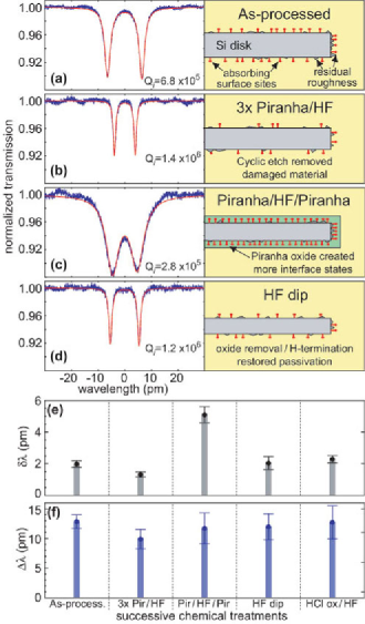
The stark difference between the surface-sensitive TM and bulk TE modes indicates that the as-processed Si surfaces are far from optimal. Etch-induced surface damage on the microdisk sidewall can only account for a small fraction of this difference due to the enhanced sensitivity of the TM1,m to the top and bottom Si surfaces (comparison of the TM and TE modes in the same microdisk and with similar modal overlap with the microdisk edge bear this out). Damage to the top and bottom Si surfaces can stem from a variety of possible sources including chemical mechanical polishing, native oxide formation during storage, or adventitious organic matterFenner . In an attempt to repair the Si surfaces a series of chemical oxidation treatments were performed on the devices. The well-known process Chabal ; Linnros ; Sparacin of repeated chemical oxidation in Piranha (H2SO4/H2O2) and HF oxide stripping was employed to controllably prepare the Si surfaces. Three cycles of the Piranha/HF process, recipe shown in Table 1, were applied to the as-processed devices. From the blue-shift in the WGM resonances due to the three cycles of the Piranha/HF process, an estimated nm of Si was removed from the surface of the microdisk. The fit to the TM1,31 transmission spectrum, shown in Figure 3(b), indicates that a significant improvement to the surfaces has also taken place, yielding a pm and pm.
To separate the effects of the Piranha oxidation and the HF etch, the sample was put through a Piranha/HF/Piranha treatment. The first cycle of Piranha/HF was used to “refresh” the hydrogen passivation before re-oxidizing the Si surface with Piranha. Figure 3(c) shows the fit to the now barely resolvable TM1,31 doublet yielding pm and pm. The five-fold increase in linewidth and a negligible increase in doublet splitting is indicative of a significant activation of absorbing surface states without an increase in surface scattering. Removing the chemical oxide with the HF dip listed in Table 1 and retesting indicated that an oxide film equivalent to nm of SiO2 had been present. The fit to the transmission spectrum of the TM1,31 mode in Figure 3(d) yielded fit parameters pm and pm, showing that the optical damage to the Si surfaces caused by Piranha oxidation was reversible.
As a final treatment to the m radii microdisks, we used the same oxidation and stripping process as described in Table 1, but with an HCl based chemistry (8:1:2 H20:HCl:H2O2, heated to C) instead of the H2SO4 based chemistry. Figure 3(e-f) shows a graphical representation of the average behavior of all TM1,m modes in the - nm span after each chemical treatment. The results reveal that the HCl oxidation was slightly less effective at passivating the silicon surface than the Piranha oxidation; however, it is expected that the optimum solution for chemical oxidation will depend upon the Si crystal orientation and previous chemical treatmentsPetitdidier ; Kobayashi .
| Step | Composition111All ratios are quoted by volume of standard concentration aqueous solutions | Temp. | Time |
|---|---|---|---|
| Piranha | 3:1 H2SO4/H2O2 | C | 10 min |
| Rinse | DI H2O | C | 30 sec |
| Rinse | DI H2O | C | 30 sec |
| Rinse | DI H2O | C | 30 sec |
| HF dip | 10:1 H2O/HF | C | 1 min |
| Rinse | DI H2O | C | 15 sec |
| Rinse | DI H2O | C | 15 sec |
Although it has recently been observedSparacin that repeated chemical oxidation and removal of silicon can provide a smoothing action on etched sidewalls, the large shifts in optical loss with chemical treatment described above can be linked to surface-state absorption as opposed to surface-scattering. Whereas the highly confined Si waveguide measurements to date have been sensitive to changes in loss as low as dB/cm, the microdisks of this work are sensitive to changes of loss more than an order of magnitude smaller ( dB/cm) where surface chemistry is more likely to play a role. Indeed, as mentioned above the TM-polarized microdisk WGMs are selectively sensitive to the top and bottom Si surfaces which are extremely smooth in comparison to etched surfaces. The negligible change in average mode-splitting, , with chemical treatment (Figure 3(f)) is also indicative of little change in surface roughness.
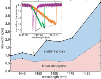
In order to confirm the above assumption, and to measure the efficacy of the surface-state passivation of the Piranha/HF chemistry, the wavelength dependent optical quality was measured on m radii disks subjected to a Piranha/HF treatment. FEM simulations show that m radii disk have approximately the same fractional energy overlap with the top/bottom Si surfaces ( nm-1) as m radii disks but have roughly half the fractional energy overlap with the etched sidewalls ( nm-1). Figure 4 shows a plot of the wavelength dependent loss across the full nm span for the TM1,m modes of a m radius disk, showing a strong trend towards increasing optical loss with wavelength. The black line indicates the intrinsic linewidth for each number, with an error bar of pm per point (not shown). The separation of scattering loss and linear absorption was obtained using a modified version of the power dependent measurements described in Reference Borselli2 . This technique uses the local temperature increase of the silicon microdisk to determine the absorption component of loss, similar to PDS, but without the need for a thermal model for heat flow; rather, the onset of two-photon absorption changes the fraction of absorption as a function of power, allowing the linear absorption coefficient to be ascertained directly. The inset to Fig. 4 shows three examples of power dependent transmission spectra for the nm mode (grey arrow), along with corresponding transmission minima versus wavelength (black dots).
From the optical loss measurements of Fig. 4 it is clear that a significant fraction of residual optical loss, after Piranha/HF treatment and hydrogen surface passivation, is still due to surface-state absorption (bulk absorption is negligible at this level). The strong trend of increasing optical loss with wavelength is seen to be dominated by elastic scattering and/or radiation loss, with the surface-state absorption being relatively constant across the - nm spectrum. Through measurements of the radiation limited quality factors of TM1,m modes in the longer wavelength - nm band, intrinsic radiation losses from the circular microdisk are found to contribute negligibly to the losses in Fig. 4. FEM simulations also show that on all of the surfaces changed less than over the - nm span. The most likely explanation for the observed wavelength dependant loss is improved phase-matching of surface-scattering into radiation modes with increasing wavelength.
By comparing the cavity before and after the Piranha oxide removal, a fractional surface absorption loss per pass of is estimated for the Piranha oxide. This large fractional absorption in the nm wavelength band ( eV) is attributed to single-photon absorption by mid-gap interface states. Such electronic interface states at the Si/(Piranha)SiOx interface have been observed in Ref. Yamashita , with three sets of state-density maxima in the bandgap of silicon occurring at , , and eV above the valence-band maximum. In comparison, from Figure 4, the modal absorption loss of the hydrogen-passivated Si surface is as small as cm-1, corresponding to a fractional surface absorption loss per pass of for the top (bottom) Si active layer surface.
All of the measurements described above were performed in a N2 purged environment over several weeks. Even in such an environment, however, changes in the hydrogen passivated surfaces were observed over times as short as a few days. Left in an unprotected air environment, degradation of the optical surface quality was evident in a matter of hours. Research and development of stable surface passivation techniques optimized for optical quality, akin to the gate oxides of CMOS microelectronics, will be a key ingredient in the future development of Si photonics. Our data suggests that surface chemistry as much as surface roughness will ultimately limit the performance of Si microphotonic devices, and further development of Si passivation techniques should be able to reduce optical losses by as much as an order of magnitude (towards the bulk -Si limit) while simultaneously improving the stability and manufacturability of future Si photonic components.
References
- (1) Yablonovitch, E., Allara, D. L., Chang, C. C., Gmitter, T. & Bright, T. B. Unusually low surface-recombination velocity on silicon and germanium surfaces. Phys. Rev. Lett. 57, 249–252 (1986).
- (2) Chabal, Y., Higashi, G. & Raghavachari, K. Infrared spectroscopy of si(111) and si(100) surfaces after hf treatment: Hydrogen termination and surface morphology. J. Vac. S. Tech. A 7, 2104–2109 (1989).
- (3) Fenner, D., Biegelsen, D. & Bringans, R. Silicon surface passivation by hydrogen termination: A comparative study of preparation methods. J. Appl. Phys. 66, 419–424 (1989).
- (4) Yamashita, Y., Asano, A., Nishioka, Y. & Kobayashi, H. Dependence of interface states in the si band gap on oxide atomic density and interfacial roughness. Phys. Rev. B 59, 872–881 (1999).
- (5) Kobayashi, H., Yamashita, Y., Nakato, Y., Komeda, T. & Nishioka, Y. Interface states at ultrathin oxide/si(111) interfaces obtained from x-ray photoelectron spectroscopy measurements under biases. Appl. Phys. Lett. 69, 2276–2278 (1996).
- (6) Linnros, J. Carrier lifetime measurements using free carrier absorption transients. ii. lifetime mapping and effects of surface recombination. J. Appl. Phys. 84, 284–291 (1998).
- (7) Li, F., Balazs, M. K. & Anderson, S. Effects of ambient and dissolved oxygen concentration in ultrapure water on initial growth of native oxide on a silicon (100) surface. J. Electrochem. Soc. 152, G669–G673 (2005).
- (8) Petitdidier, S. et al. Growth mechanism and characterization of chemical oxide films produced in peroxide mixtures on si(100) surfaces. Thin Solid Films 476, 51–58 (2005).
- (9) Muller, D. A. A sound barrier for silicon? Nature Materials 4, 645–647 (2005).
- (10) Liu, A. et al. A high-speed silicon optical modulator based on a metal-oxide-semiconductor capacitor. Nature 427, 615–618 (2004).
- (11) Xu, Q., Schmidt, B., Pradhan, S. & Lipson, M. Micrometre-scale silicon electro-optic modulator. Nature 435, 325–327 (2005).
- (12) Boyraz, O. & Jalali, B. Demonstration of a silicon raman laser. Opt. Express 12, 5269–5273 (2004).
- (13) Rong, H. et al. A continuous-wave raman silicon laser. Nature 433, 725–728 (2005).
- (14) Notomi, M. et al. Optical bistable switching action of Si high- photonic-crystal nanocavities. Opt. Express 13, 2678–2687 (2005).
- (15) Tanabe, T., Notomi, M., Mitsugi, S., Shinya, A. & Kuramochi, E. Fast bistable all-optical switch and memory on a silicon photonic crystal on-chip. Opt. Lett. 30, 2575–2577 (2005).
- (16) Song, B., Noda, S., Asano, T. & Akahane, Y. Ultra-high-q photonic double-heterostructure nanocavity. Nature Materials 4, 207–210 (2005).
- (17) Vahala, K. J. Optical microcavities. Nature 424, 839–846 (2003).
- (18) Lang, D. V. Deep-level transient spectroscopy: A new method to characterize traps in semiconductors. J. Appl. Phys. 45, 3023–3032 (1974).
- (19) Chantre, A., Vincent, G. & Bois, D. Deep-level optical spectroscopy in gaas. Phys. Rev. B 23, 5335–5358 (1981).
- (20) Aarts, I. M. P. et al. Direct and highly sensitive measurement of defect-related absorption in amorphous silicon thin films by cavity ringdown spectroscopy. Appl. Phys. Lett. 84, 3079–3081.
- (21) Jackson, W. B. & Amer, N. M. Direct measurement of gap-state absorption in hydrogenated amorphous silicon by photothermal deflection spectroscopy. Phys. Rev. B 25, 5559–5562 (1982).
- (22) Amato, G. & Fizzotti, F. Gap-states distribution in amorphous-silicon films as obtained by photothermal deflection spectroscopy. Phys. Rev. B 45, 14108–14113 (1992).
- (23) Blood, P. On the dimensionality of optical absorption, gain, and recombination in quantum-confined structures. IEEE J. Quan. Elec. 36, 354–362 (2000).
- (24) Spillane, S. M. et al. Ultrahigh-q toroidal microresonators for cavity quantum electrodynamics. Phys. Rev. A 71, 013817 (2005).
- (25) Teraoka, I., Arnold, S. & Vollmer, F. Perturbation approach to resonance shifts of whispering-gallery modes in a dielectric microsphere as a probe of a surrounding medium. J. Opt. Soc. Am. B 20, 1937–1946 (2003).
- (26) Borselli, M., Johnson, T. J. & Painter, O. Beyond the rayleigh scattering limit in high- silicon microdisks: theory and experiment. Opt. Express 13, 1515–1530 (2005).
- (27) Borselli, M., Srinivasan, K., Barclay, P. E. & Painter, O. Rayleigh scattering, mode coupling, and optical loss in silicon microdisks. Appl. Phys. Lett. 85, 3693–3695 (2004).
- (28) Gorodetsky, M., Pryamikov, A. & Ilchenko, V. Rayleigh scattering in high-q microspheres. J. Opt. Soc. Am. B 17, 1051–1057 (2000).
- (29) Little, B. E., Laine, J.-P. & Chu, S. T. Surface-roughness-induced contradirectional coupling in ring and disk resonators. Opt. Lett. 22, 4–6 (1997).
- (30) Sparacin, D. K., Spector, S. J. & Kimerling, L. C. Silicon waveguide sidewall smoothing by wet chemical oxidation. J. Lightwave Tech. 23, 2455–2461 (2005).