Pixel Detectors
††thanks: Work supported by the German Ministerium für Bildung, und Forschung (BMBF) under contract no. and by the DIP Foundation under contract no. E7.1address: Physikalisches Institut, Nussallee 12, D-53115 Bonn, Germany, Tel.: +49 228 73-3533, Fax: -3220, email: wermes@uni-bonn.de
Abstract
Pixel detectors for precise particle tracking in high energy physics have been developed to a level of maturity during the past decade. Three of the LHC detectors will use vertex detectors close to the interaction point based on the hybrid pixel technology which can be considered the ‘state of the art ‘ in this field of instrumentation. A development period of almost 10 years has resulted in pixel detector modules which can stand the extreme rate and timing requirements as well as the very harsh radiation environment at the LHC without severe compromises in performance. From these developments a number of different applications have spun off, most notably for biomedical imaging. Beyond hybrid pixels, a number of monolithic or semi-monolithic developments, which do not require complicated hybridization but come as single sensor/IC entities, have appeared and are currently developed to greater maturity. Most advanced in terms of maturity are so called CMOS active pixels and DEPFET pixels. The present state in the construction of the hybrid pixel detectors for the LHC experiments together with some hybrid pixel detector spin-off is reviewed. In addition, new developments in monolithic or semi-monolithic pixel devices are summarized.
1 Hybrid pixel detectors for the LHC experiments
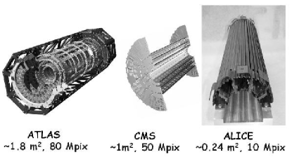
The truly challenging requirements on detectors operation close to the interaction points at the LHC are on spatial resolution, on timing precision, and most importantly on the long term operation performance and radiation tolerance to particle fluences as high as ncm-2. At present, these demands are only met by so-called hybrid pixel detectors, for which the particle sensing element, the sensor, and the integrated electronics circuitry, the readout chip, are separate entities. They are mated by a hybridization technique, known as bump and flip-chip technology. All of the LHC-collider-detectors ALICE [1, 2], ATLAS [3, 4], and CMS [5, 6], LHCb (for the RICH system) [7] at the LHC, and the CERN fixed target experiment NA60 [8], employ the hybrid pixel technique to build large scale (up to 2m2) pixel detectors. Pixel area sizes are typically 50 400 m2 as for ATLAS or 100 150 m2 as for CMS. The detectors are arranged in cylindrical barrels of 2 to 3 layers and disks covering the forward and backward regions.
1.1 The sensors
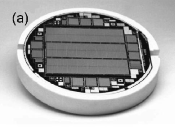
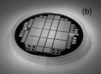
The discovery that oxygenated silicon is more radiation hard, with respect to the non-ionizing energy loss of protons and pions [9] than standard silicon, allows operation of pixel detectors at the LHC for which the radiation is most severe due to their proximity to the interaction point. Sensors with electrodes in n-bulk material have been chosen to cope with the fact that type inversion occurs after about cm-2. After type inversion to p-type bulk material the -diode sits on the electrode side, from which the depletion zone develops into the bulk, thus allowing the sensor to be operated partially depleted. For the Super-LHC, a name termed for an LHC-upgrade programme which targets a luminosity of 1035cm-2s-1 and hence scales the environment at the LHC by a factor ten in all aspects, new sensor technologies are needed to cope with the radiation hardness demands. Figures 1(a) and (b) show photographs of the sensor wafers of ATLAS and CMS, respectively, which both use oxygenated silicon as the sensor material.
1.2 The FE electronics
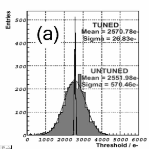
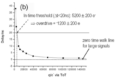
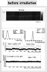
The challenge in the design of the front-end pixel electronics [10] can be summarized by the following requirements: low power ( 50W per pixel), low noise and threshold dispersion (together 200e), zero suppression in every pixel, on-chip hit buffering, and small time-walk to be able to assign the hits to their respective LHC bunch crossing. The pixel groups at the LHC have reached these goals in several design iterations using first radiation-soft prototypes, then dedicated radhard designs, and finally using deep submicron technologies. For ATLAS the full production quantity of chip wafers has been processed and tested with an average yield of 82. CMS yields are in the same order and ALICE chip yields are 51 with a chip area of 13.5 15.8 mm2. While CMS uses analog readout of hits, ATLAS obtains pulse height information by means of measuring the time over threshold (ToT) for every hit. Figure 2(a) shows the distribution of measured thresholds of an ATLAS front-end chip. The dispersion of about 600 e- can be lowered to below 50 e- by a 7-bit tuning feature implemented in the chip. Figure 2(b) illustrates the effect of time walk for small signals. For efficient signal detection within a defined time of 20 ns with respect to the bunch crossing an overdrive of about 1200 is necessary. The bunch crossing occurs every 25 ns.
The hit information is extracted as follows: A 40 MHz Gray coded clock is transmitted to all pixel cells. If the pixel circuit detects a hit signal (analog) it generates digital hit information. The hit data (address and time stamp) are transmitted to the bottom of the chip and temporarily stored in end of column buffers outside pixel matrix. The buffers monitor the age of each hit data and delete hits when no trigger coincidence occurs. Hits having their time stamp coincident with the LV1 trigger are finally read out.
1.3 Hybridization
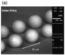
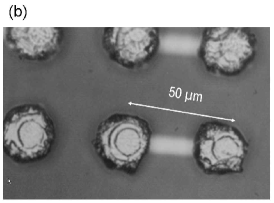
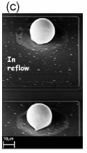
Hybridization of chip and sensor is done by fine pitch bumping and subsequent flip-chipping, either with PbSn (solder) or with Indium bumps. The Indium bumps are applied by a wet lift-off technique and can be mated by direct thermo-compression [11, 12] or reflown, as developed by CMS [13]. After bumping the chips are thinned by backside grinding to a thickness of 150 - 180 m. Fig. 4 shows rows of m pitch bumps obtained by these techniques. All of these bump bonding technologies have been successfully used with 8” IC-wafers and 4” sensor wafers.
ATLAS pixel modules are hybridized by two vendors (one using indium one solder) at a rate of about up to 2 20 per week. The fraction of broken, bridged or missing bumps is at the level of 10-4. Above 85 of all modules have less than 0.1 of bad bumps. About 10-15 of the modules arriving from the vendor have a chip with an unacceptably high number of bump failures and need to be reworked, i.e. removing the FE-chip from the module and flip-chipping of a new one. The success fraction of this operation is 99 for solder and 80 for indium, mostly due to the fact that In-bumps are flatter and remnants of dirt in the reworking process do more harm. The total reject fraction of modules to date is 1 and 14 [14] for PbSn- and Indium bumped modules, respectively.
1.4 The modules
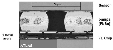
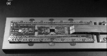
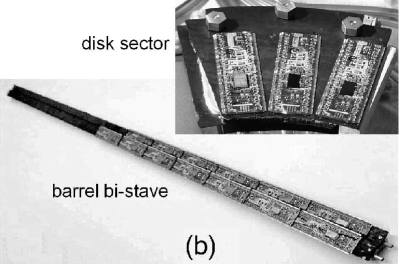
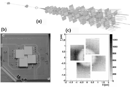
The CMS and ATLAS modules (cf Fig. 5(a)) typically have 2 cm 6.5 cm area consisting of 16 FE-chips bump-connected to one silicon sensor.The I/O lines of the chips are connected via wire bonds to a kapton flex circuit glued atop the sensor. The flex houses a module control chip responsible for front end time/trigger control as well as event building. The total thickness at normal incidence is in excess of . The modules are arranged in barrel-ladders or disk-sectors as shown in Fig. 5(b) for the case of ATLAS.
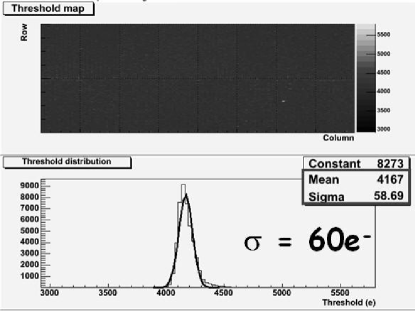
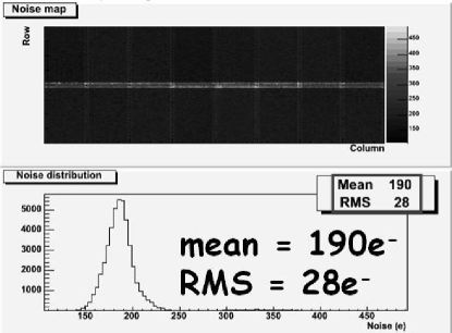
Production pixel modules are scrutinized by extensive tests in the lab, among them their analog and digital functionality, noise and threshold performance, response to an X-ray source scan, as well as temperature cycling of modules and also of assembled ladders. For ATLAS modules, after tuning the threshold spread is well below 100 and the mean value of the noise distribution is between 150 and 200 (cf. Fig. 6). The quadratic sum of both is many sigmas away from the typical threshold setting of 3000 or above, a requirement at LHC in order to keep the noise hit occupancy low. In order to qualify the modules for their placement inside the ATLAS pixel detector arrangement, a ranking factor based on pixel efficiency, sensor quality, noise and threshold performance, and rework penalty is introduced and a cut is placed to qualify the modules as barrel layer B, 1, or 2 or as disk modules. Based on a sample of about 1300 modules to date 54 of the produced modules meet the most demanding qualification as B-layer modules. Finally, complete ladders of 13 module undergo a so-called system test, i.e. a test procedure involving the complete readout chain of ATLAS, including micro-cables, conversion into optical signal and clock transmission and their routing over the full cable length in ATLAS. Comparison to module stand-alone tests show no significant chances in the performance.
1.5 Radiation tolerance
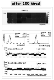
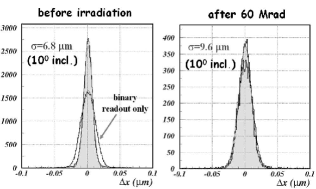
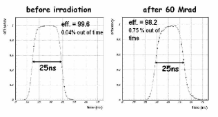
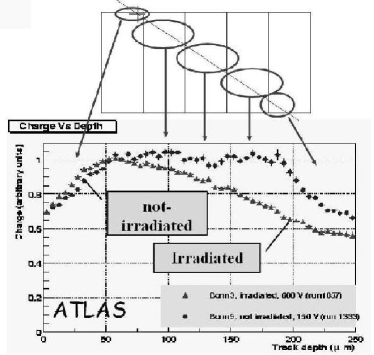
Most challenging at LHC is the requirement on radiation tolerance of the pixel detector which is exposed to (mostly) pion fluences of 10 n/cm2 or 500 kGy during 10 years of LHC operation. The advancement of oxygenated silicon and deep submicron chip technology made a long life time in such an environment possible. Figures 7(a)-(c) show the comparison of critical performance figures before and after irradiation of ATLAS pixel modules. In parts the received dose of the modules was well in excess of that expected for 10 years operation at the LHC. After irradiation to 500 kGy the mean collected charge fraction has been measured to be 80 and the in-time efficiency, i.e. the efficiency for hit detection within 20ns after the bunch crossing, is 97.80.1. An important characterization figure is the in-time efficiency, which in test beams, at which the arrival of the beam particles is asynchronous to the system clock, can be determined by plotting the hit efficiency as a function of the delay between the arrival time and the clock edge, measured by a TDC. It is mandatory that a high efficiency is reached somewhere inside a plateau. The width and flatness of the plateau is a measure of some kind of margin that exists. The plateau width decreases after irradiation from originally 14 ns to 9.7 ns. Figure 8 shows a comparison between irradiated and not irradiated pixel sensors regarding the amount of trapping. By measuring the charge collection efficiency under inclined angles different depths for the charge deposition in the sensor can be addressed and hence trapping can be studied as shown by Fig. 8. After 10 years at the LHC the charge collection efficiency is about 80. The charge yield as a function of depth can be translated into an electron carrier life time of = 4.1 0.6 ns.
1.6 Support structures and total thickness
For ALICE the demands imposed by the physics are different than for ATLAS and CMS. While the track density (80 hits/cm2) with 8000 charged particles per rapidity interval for central heavy ion collisions is truly formidable, the radiation level of 5 kGy or 61012neq/cm2, due to the much lower collision rate, is much lower than for pp collisions. As a consequence cooling to temperatures below 0∘C as for CMS and ATLAS is not mandatory, but instead very thin materials for a small total radiation length are aimed for. The reduced cooling requirement (24∘ C) allows the use of a very light weight structure with 40m wall thickness PHYNOX tubes and a total contribution of 0.3X0. Together with thin sensors (200 m) and chips (150 m) an ALICE module (1.28 cm 7.0 cm, 5 readout chips bonded to one sensor) arrives at a total radiation length per layer of only 0.9.
1.7 LHC pixels put to test in NA60
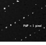
The CERN heavy ion experiment NA60 [15] has used LHC-type pixel detectors for the first time in a running experiment. The setup of the NA60 pixel tracker is shown in Fig. 10 (top). For the initial running the ALICE-LHCb chip was used. Eight 4-chip (Fig. 10(bottom left)) and eight 8-chip planes provide track reconstruction with 12 pixel hits on a track. The sensors have been exposed to a radiation dose of 120 kGy and were operated through type inversion. Due to the inhomogeneous irradiation the inner part of the planes has received a larger dose than the outer, which is demonstrated by the hit multiplicity pattern taken with a lowered bias voltage in Fig. 10(bottom right). The improvement in physics from the operation of the pixel vertex detector has been reported in [15]. The Indium target position can be resolved to 20m in the direction transverse to the beam and 200m in the longitudinal direction. The meson resonances and could be detected with a resolution of 23 MeV in the di-muon invariant mass. In 2005, data for p-nucleus running at a beam intensity of 2109 p/burst and an interaction rate of one per 25 ns has been taken. In order to cope with such LHC-like data rates, four planes using ATLAS production modules were added to the setup.
2 Spin-off from hybrid pixel detectors into other fields
2.1 X-ray imaging using counting pixel detectors
Spin-off from hybrid pixel detectors in particle physics has most directly arisen in imaging applications as detectors that accumulate the incident radiation by the counting of individual radiation quanta in every pixel cell. This technique offers many features which are very attractive for X-ray imaging: full linearity in the response function, in principle an infinite dynamic range, optimal exposure times and a good image contrast compared to conventional film-foil based radiography, thus avoiding over- and under-exposed images. The analog part of the pixel electronics is in parts close to identical to the one for LHC pixel detectors while the periphery has been replaced by counting circuitry [16]. The same principle is also used for protein-crystallography with synchrotron radiation [17, 18].
The challenges which are to be addressed in order to be competitive with integrating systems are: high speed ( 1 MHz) counting with a range of at least 15 bits, operation with very little dead time, low noise and particularly low threshold operation with small threshold dispersion values. In particular, the last item is important in order to allow homogeneous imaging of soft X-rays of energies in the energy range below 10 keV. It is also mandatory for a differential energy measurement, realized so far as a double threshold with energy windowing logic [19, 20, 21], which can enhance the contrast of an image as the shape of the X-ray energy spectrum is different behind different absorbers (e.g. bone or soft tissue). Finally, for radiography, high photon absorption efficiency is mandatory, requiring the use and development of high-Z sensors and their hybridization.
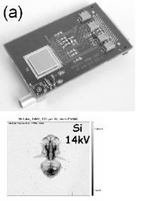
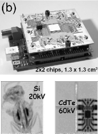
The MEDIPIX collaboration [21] uses the MEDIPIX2 chip with , 5555 m2 pixels fabricated in a m technology, energy windowing via two tunable discriminator thresholds, and a 13 bit counter. The maximum count rate per pixel is about 1 MHz. Fig. 11(a) a single chip module together with an image of a bee taken using 14 keV X-rays [21]. A Multi-Chip module with 2x2 chips using high-Z CdTe sensors is shown in Fig. 11(b) using the MPEC chip [22], together with two X-ray images. The MPEC chip features pixels (200200m2), double threshold operation, 18-bit counting at 1 MHz per pixel as well as low noise values (120e with CdTe sensor) and threshold dispersion (e after tuning) [23, 22]. A technical issue here is the bumping of individual die CdTe sensors which has been solved using Au-stud bumping with Indium-filling [24].
2.2 Counting pixels in protein crystallography
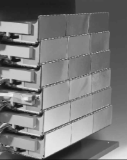
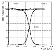
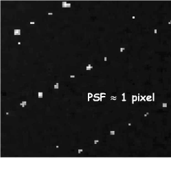
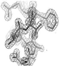
In protein crystallography with synchrotron radiation [17] the challenge is to image many thousands of Bragg spots from X-ray photons with energies of 12 keV (corresponding to resolutions at the 1 range) or higher, scattering off protein crystals. This must be accomplished at a high rate (1-1.5 MHz/pixel) and by systems with a high dynamic range. The typical spot size of a diffraction maximum is m, calling for pixel sizes in the order of m. The high linearity of the hit counting method and the absence of so-called ”blooming effects”, i.e. the response of non-hit pixels in the close neighborhood of a Bragg spot, makes counting pixel detectors very appealing for protein crystallography experiments. Counting pixel developments are made for the ESRF (Grenoble, France) [25] and the SLS (Swiss Light Source at the Paul-Scherrer Institute, Switzerland) beam lines. A photograph of the PILATUS 1M detector [26] at the SLS ( 106 mm pixels, 18 modules, 2024 cm2 area) is shown in Fig. 12(a). A systematic limitation and difficulty is the problem that homogeneous hit/count responses in all pixels, also for hits at the pixel boundaries or between pixels where charge sharing plays a role must be maintained by delicate threshold tuning (cf Fig. 12(b)). Fig. 12(c) shows a flat-field image obtained with a PILATUS module, which demonstrates that this principle problem can be overcome [27]. Figure 12(d), shows some Bragg spots obtained with a 10s exposure to 12 keV synchrotron X-rays [28]. Some spots are contained in only one pixel, others spread over a few pixels due to charge sharing. This demonstrates the intrinsically good point resolution of the system. Figure 12(e) is a reconstructed electron density map of the thaumtin crystal [27]. Alternative developments which aim to improve the active/inactive area ratio for protein-crystallography X-ray detection are so-called 3-D silicon sensors (strip or pixels) [29]. A detailed account can be found in [30].
3 Challenges imposed by a Super-LHC
The radiation levels expected at an LHC upgrade, called Super-LHC or SLHC, are a factor of ten higher than at the LHC, i.e. to 1016neq/cm2. There are mainly three effects as a consequence [31].
-
1.
A change of the effective doping concentration (higher depletion voltage necessary, under-depletion)
-
2.
An increase of leakage current (increase of shot noise, thermal runaway)
-
3.
An increase of charge carrier trapping (loss of charge)
Several routes to cope with this are being pursued, among them the development of even more radiation hard silicon based on oxygenated float-zone (DOFZ), Czochralski (Cz) and epitaxial silicon [31]. For this review I would like to address in this context two new approaches which are more linked to pixel detectors: diamond pixel detectors and 3D-silicon devices.
3.1 Diamond Pixels
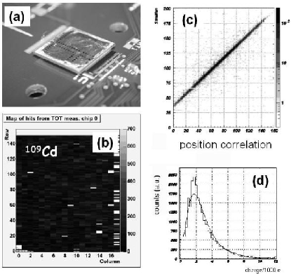
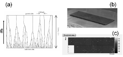
CVD-Diamond as a sensor material has been developed by the CERN RD group RD42 for many years [32]. Charge collection distances approaching 300 m has also triggered the development of a hybrid pixel detector using diamond as sensors [33, 34]. The non-uniform field distribution inside CVD-diamond, which originates from the grain structure in the charge collecting bulk (cf. Fig. 14(a)) introduces polarization fields inside the sensor due to charge trapping at the grain boundaries which superimpose on the biasing electric field. This results in position dependent systematic shifts in the track reconstruction with a typical average grain size of 100m - 150m [35]. Diamond sensors with charge collection distances in excess of 300m have been fabricated and tested [36]. Single chip pixel modules as well as a full size wafer scale 16-chip module assembled using ATLAS front-end chips have been built and tested. Figure 13(a) and (b) show the diamond pixel detector and a hit response pattern obtained by exposing the detector to a 109Cd source of 22 keV rays, which deposits approximately 1/4 of the charge of a minimum ionizing particle. The single chip module has been tested in a high energy (180 GeV) pion beam at CERN, the module in a 4 GeV electron beam at DESY. Figure 13(c) and (d) show position correlation and the charge distribution of the diamond pixel detector in a high energy beam, respectively. A spatial resolution of = 12m has been measured with the single chip module at high energies with 50m pixel pitch. A technical challenge to produce a wafer scale module lies in the hybridization process, i.e. bump deposition and flip-chipping. Figure 14 shows the 16-chip diamond module (Fig. 14(b)) and its tuned threshold map (Fig. 14(c)) with a very small dispersion of only 25e- and good bump yield homogeneity. One chip was damaged during test beam by electrostatic discharge. The rms of the position residuals was measured to 24 m in the DESY 6 GeV beam [34]. This value is dominated by the multiple scattering contribution from the beam telescope.
3.2 3D silicon sensors
So-called 3D silicon detectors have been developed [29] to overcome several limitations of conventional planar Si-pixel detectors, in particular in high radiation environments, in applications with inhomogeneous irradiation and in applications which require a large active/inactive area ratio such as protein crystallography [18].
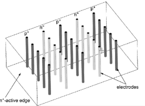
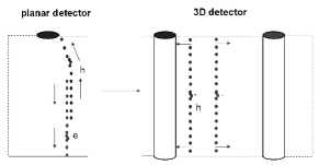
A a 3D-Si-structure (Fig. 15(a)) is obtained by processing the n+ and p+ electrodes into the detector bulk rather than by conventional implantation on the surface. This is done by combining VLSI and MEMS (Micro Electro Mechanical Systems) technologies. Charge carriers drift inside the bulk parallel to the detector surface over a short drift distance of typically 50m. Another feature is the fact that the edge of the sensor can be a collection electrode itself thus extending the active area of the sensor to within few m to the edge. Edge electrodes also avoid inhomogeneous fields and surface leakage currents which usually occur due to chips and cracks at the sensor edges. The main advantages of 3D-silicon detectors, however come from a different way of charge collection and the fact that the electrode distance is short (50m) in comparison to conventional planar devices at the same total charge, This results in a fast (1-2 ns) collection time, low ( 10V) depletion voltage and, with edge electrodes in addition, a large active/inactive area ratio of the device (cf. Fig. 15(b)).
The technical fabrication is much more involved than for planar processes and requires a bonded support wafer and reactive ion etching of the electrodes into the bulk. A compromise between 3D and planar detectors, so called planar-3D detectors maintaining the large active area, use planar technology but with edge electrodes [37], obtained by diffusing the dopant from the deeply etched edge and then filling it with poly-silicon. Prototype detectors using strip or pixel electronics have been fabricated and show encouraging results with respect to speed (3.5 ns rise time) and radiation hardness ( 1015 protons/cm2) [38]. 3D-pixel detectors with LHC-type frontend electronics have not been successfully built yet, although the hybridization imposed no problem compared to standard hybrid pixel devices. A fabrication of 3D-pixel structures adapted to the ATLAS FE-chip is underway [39].
4 Monolithic and Semi-Monolithic Pixel Detectors
Monolithic pixel detectors, in which amplifying and logic circuitry as well as the radiation detecting sensor are one entity, are in the focus of present developments. To reach this ambitious goal, optimally using a commercially available and cost effective technology, would be another breakthrough in the field. The present developments have been much influenced by RD for vertex tracking detectors at future colliders such as the International Linear Collider (ILC) [40]. Very low (1 X0) material per detector layer, small pixel sizes (20mm) and a high rate capability (80 hits/mm2/ms) are required, due to the very intense beamstrahlung of narrowly focussed electron beams close to the interaction region, which produce electron positron pairs in vast numbers. High readout speeds with typical line rates of several MHz and a 40s frame readout time are necessary.
At present, two developments have already reached some level of maturity: so called CMOS active pixels and DEPFET pixels. Other promising approaches, not mentioned in this review, are amorphous a-Si:H layers for charge collection superimposed on standard CMOS ASICS [41] as well as so called SOI-sensors [42], which use a high-ohmic Si-substracte with full charge collection wafer-bonded to a CMOS electronics layer. Both active layers (sensor and CMOS) are isolated by an insulating layer through which a via-contact is made. These concepts are still in their early development phases but offer new possibilities once larger scale production is mastered.
4.1 CMOS active pixels
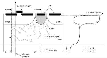
In some CMOS chip technologies a lightly doped epitaxial silicon layer of a few to 15m thickness between the low resistivity silicon bulk and the planar processing layer can be used for charge collection [43, 44, 45]. The generated charge is kept in a thin epi-layer atop the low resistivity silicon bulk by potential wells that develop at the boundary and reaches an n-well collection diode by thermal diffusion (cf. Fig. 16(a)). With small pixel cells collection times in the order of 100 ns are obtained. The charge collecting epi-layer is – technology dependent – at most 15m thick and can also be completely absent. The attractiveness of active CMOS pixels lies in the fact that standard CMOS processing techniques are employed and hence they are potentially very cheap. CMOS active pixel sensor development are pursued by many groups which partially collaborate in various projects (BELLE-upgrade,STAR-upgrade,ILC,CBM at GSI) who use similar approaches to develop large scale CMOS active pixels, also called MAPS (Monolithic Active Pixel Sensors) [44]. A recent review can be found in [46]. The sensor is depleted only directly under the n-well diode. The signal charge is hence very small (1000e) and full charge collection is obtained only in the depleted region under the n-well electrode (cf Fig. 16(b)). Low noise electronics is therefore the challenge in this development.
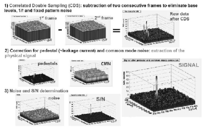
Matrix readout of MAPS is performed using a standard 3-transistor circuit (line select, source-follower stage, reset) commonly employed by CMOS matrix devices, but can also include current amplification and current memory [47]. In the active ares only nMOS transistors are permitted because of the n-well/p-epi collecting diode which does not permit other n-wells. For an image two complete frames are subtracted from each other (correlated double sampling, CDS) to eliminate base levels, 1/f and fixed pattern noise (see Figure 17). In a second step pedestals and common mode noise are subtracted to extract the signal and to determine the remaining noise. Detector sizes up to 19.417.4 mm2 with 1M pixels have been tested. The smallest pixel pitch was 17m. Frame speeds of 10s for 132x48 pixels have been reached for the BELLE development, with a noise figure of 30-50e- [48]. With other pixel matrices with slower readout noise values of 15-20 e-, S/N ratios larger than 20 and spatial resolutions of 1.5m (5m) for 20m (40m) pitch have been measured [46].
The presently favored technology is the AMS 0.35m OPTO process, which possesses a 10m thick epitaxial layer. Regarding radiation hardness MAPS appear to sustain non-ionizing radiation (NIEL) to 1012neq. The effects of ionizing radiation damage (IEL), the main damage source at the ILC, are threshold shifts and leakage currents in and between nMOS transistors. The damage effects are less severe when short readout integration times (10s) are used. This way doses of about 10 kGy can be tolerated [46].
The present focus of further development lies in improving the radiation tolerant design, making 50m thin detectors, making larger area devices for instance by stitching over reticle boundaries [49], and increasing the charge collection performance in the epi-layer by triple-well [50] or other techniques [51, 52, 53].
4.2 DEPFET pixels
In so-called DEPFET pixel sensors [54] FET transistor is implanted in every pixel on a sidewards depleted [55] bulk. Electrons generated by radiation in the bulk are collected in a potential minimum underneath (m) the transistor channel (internal gate) thus modulating its current (Fig. 18).
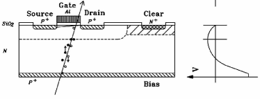
Electrons collected in the internal gate are completely [56] removed by a clear pulse applied to a dedicated contact outside the transistor. Amplification values of 300 pA per collected electron in the internal gate have been achieved. Further current amplification and storage enters at the second level stage. The bulk is fully depleted yielding large signals and the small capacitance of the internal gate offers low noise operation, for a very large S/N ratio. This in turn can be used to fabricate very thin devices. Thinning of pn-diodes to a thickness of 50m using a technology based on wafer bonding and deep anisotropic etching has been successfully demonstrated [57].
DEPFET pixels are being developed for three very different application areas: vertex detection in particle physics [58, 59, 60], X-ray astronomy [61, 62] and for biomedical autoradiography [63]. With single pixel structures noise figures below 5e- and energy resolutions of 131 eV for 6 keV X-rays have been obtained at room temperature [64]. The challenges for an ILC vertex detector are: small pixel cells (2030m2), thin, radiation hard sensors (50m), and fast readout (10-20 MHz per matrix row of 520x4000 pixels). This is pursued by a Bonn-Mannheim-MPI Munich collaboration.
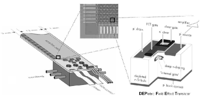
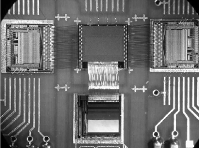
Readout of a DEPFET matrix is done by selecting a row by a gate voltage from a sequencer chip (SWITCHER) to the external gate. The drains are connected column-wise delivering their current to a current-based readout chip (CURO) with amplification and current storage at the bottom of the column [65, 64]. Both chips have been developed at close to the desired speed for a Linear Collider. A sketch of a module made of DEPFET sensors is shown in fig. 19(top). Figure 19(bottom) shows a DEPFET pixel matrix readout system used in the testbeam.
The radiation tolerance, in particular against ionizing radiation, which is expected to doses of 2 kGy due to beamstrahlung at the ILC, again is a crucial question. Irradiation with 30 keV X-rays up to doses of 10 kGy, about five times the amount expected at the ILC, have lead to transistor threshold shifts of only about 4 V. Threshold shifts of this order can be coped with by an adjustment of the corresponding gate voltages supplied by the SWITCHER chip. The estimated power consumption for a five layer DEPFET pixel vertex detector at the ILC – assuming a power duty cycle of 1:200 – is only 5W. Such a performance renders a very low mass detector without cooling pipes feasible.
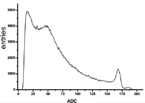
A DEPFET pixel matrix with 12864 pixels has been tested in a 6 GeV electron beam at DESY. The noise values obtained for the full system in the test beam including sampling noise of the CURO chip is 225 (see Fig. 21(a)). The S/N ratio is 144.
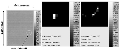
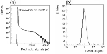
Figure 20 shows a hit in the DEPFET matrix together with two typical events with different hit clusters. The event on Fig. 20(right) is most likely explained by and consistent with the emission of a delta-ray which remains in the sensor. This also qualitatively demonstrates the good reconstruction capabilities to be expected from a DEPFET vertex detector. At 6 GeV beam energy the spatial residuals are still multiple scattering dominated. Residuals on the order of 10m are obtained, while with the large S/N value of 144 true space resolutions in the order of 2m should be possible.
5 Summary
The large pixel detectors for LHC experiments, based on the hyprid pixel technology, constitute the state of the art in pixel detector technology. These detectors are in construction and the maturity of the technology, including radiation tolerance to 500 kGy doses, has been proven. Immediate spin-off developments are hybrid pixel detectors with counting capability in which radiation quanta are individually counted. These developments open up a new approach to radiological imaging as well as to protein crystallography with synchrotron radiation. Monolithic or semi-monolithic detectors, in which detector and readout ultimately are one entity, are currently being developed in various forms, largely driven by the needs for particle detection at the ILC. Most mature at present are CMOS active pixel sensors using standard commercial technologies on low resistivity bulk, and DEPFET-pixels, which maintain high bulk resistivity for charge collection.
Acknowledgements
The author is indebted to all speakers at the PIXEL2005 conference who provided the most up-to-date material to this review.
References
- [1] The ALICE collaboration. ALICE Technical Design Report of the Inner Tracker System. CERN/LHCC/99-12, 1999.
- [2] P. Riedler et al. First results from the ALICE silicon pixel detector prototype. Nucl. Inst. and Meth., A501:111–118, 2003.
- [3] The ATLAS collaboration. Technical Design Report of the ATLAS Pixel Detector. CERN/LHCC/98-13, 1998.
- [4] C. Gemme at al. ATLAS Pixel Collaboration. The ATLAS pixel detector. Nucl. Inst. and Meth., A501:87–92, 2003.
- [5] The CMS collaboration. CMS Tracker Technical Design Report. CERN/LHCC/98-6, 1998.
- [6] W. Erdmann et al. The CMS pixel detector. Nucl. Inst. and Meth., A447:178–183, 2002.
- [7] T. Gys et al. The pixel hybrid photon detectors for the LHCb-RICH project. Nucl. Inst. and Meth., A465:240–246, 2001.
- [8] A. Baldit, J. Castor, A. Devaux, B. Espagnon, P. Force, et al. ALICE Technical Design Report of the Inner Tracker System. CERN-SPSC-2000-010, 2002.
- [9] G. Lindström et al. ROSE Collaboration. Radiation damage in silicon detectors. Nucl. Inst. and Meth., A512:92–95, 2003.
- [10] L. Blanquart et al. FE-I1: A Front-end Readout Chip Designed in a Commercial 0.25m process for the ATLAS pixel detector at LHC. IEEE Trans. Nucl. Sci., vol. 51, no. 4:1358–1364, 2004.
- [11] C. Gemme et al. Study of Indium bumping for the ATLAS pixel detector. Nucl. Inst. and Meth., A465:200–203, 2001.
- [12] A.M. Fiorello. ATLAS bump bonding process. In Pixel 2000 Conference, Genoa, Italy, June 2000.
- [13] L. Rossi, P. Fischer, T. Rohe, and N. Wermes. Pixel Detectors: From Fundamentals to Applications. Springer, Heidelberg, 2005.
- [14] A. Andreazza (ATLAS collaboration). private communication, Sept. 2005.
- [15] M. Keil et al. The NA60 pixel telescope for particle tracking in heavy-ion and proton-nucleus collisions. In PIXEL 2005 Intl. Workshop, Bonn, Sept 2005. submitted to Nucl. Instr. Meth. (2006).
- [16] P. Fischer. An area efficient 128 channel counter chip. Nucl. Inst. and Meth., A378:287–300, 1996.
- [17] H. Graafsma. Detector needs at current and future synchrotron sources. In IEEE2004 Medical Imaging Conference, Portland, USA, Oct. 2003.
- [18] E.M. Westbrook. Pixels and Proteins: Better detectors for biological crystallography. In IEEE Trans. Nucl. Sci., Portland, USA, Oct. 2003.
- [19] P. Fischer, A. Helmich, M. Lindner, N. Wermes, and L. Blanquart. A photon counting chip with energy windowing. IEEE Trans. Nucl. Sci., 47(3):881–884, 2000.
- [20] P. Fischer H. Krüger M. Lindner, L. Blanquart and N. Wermes. Medical X-ray imaging with energy windowing. Nucl. Inst. and Meth., A465:229–234, 2000.
- [21] X. Llopart, M. Campbell, R. Dinapoli, D. SanSegundo, and E. Pernigotti. MEDIPIX2: A 64-k pixel readout chip with 55m2 elements working in single photon counting mode. IEEE Trans. Nucl. Sci., 49(5):2279–2283, 2002.
- [22] M. Löcker et al. Single photon counting X-ray imaging with Si and CdTe single chip pixel detectors and multichip pixel modules. IEEE Trans. Nucl. Sci., vol. 51, no. 4:1717–1723, 2004.
- [23] P. Fischer, J. Hausmann, A. Helmich, M. Lindner, N. Wermes, and L. Blanquart. A counting pixel readout chip and sensor system for X-ray imaging. IEEE Trans. Nucl. Sci., 46(4):1070–1074, 1999.
- [24] P. Fischer, P. Fischer, M. Kouda, H. Krüger, M. Lindner, G. Sato, T. Takahashi, S. Watanabe, and N. Wermes. A counting CdTe pixel detector for hard X-ray and gamma-ray imaging. IEEE Trans. Nucl. Sci., 48(4):2401–2404, 2001.
- [25] P. Delpierre et al. Large surface X-ray pixel detector. IEEE Trans. Nucl. Sci., 49(4):1709–1711, 2002.
- [26] C. Brönnimann et al. A pixel detector for the protein crystallography beamline at the SLS. Journal of Syn. Rad., 7:301, 2000.
- [27] B. Henrich et al. Pilatus a solid state detector for x-ray sources. In PIXEL 2005 Intl. Workshop, Bonn, Sept 2005. submitted to Nucl. Instr. Meth. (2006).
- [28] E. Eikenberry et al. The PILATUS X-ray detector. In IEEE2004 Conference on Room Temperature Sensitive Devices, Portland, USA, Oct. 2003.
- [29] C. Kenney, S. Parker, J. Segal, and C. Storment. Silicon detectors with 3-D electrode arrays: fabrication and initial test results. IEEE Trans. Nucl. Sci., vol.48, no.4:1224–1236, 1999.
- [30] S. Parker et al. 3D sensors. In PIXEL 2005 Intl. Workshop, Bonn, Sept 2005. submitted to Nucl. Instr. Meth. (2006).
- [31] M. Moll. Radiation tolerant sensors for pixel detectors. In PIXEL 2005 Intl. Workshop, Bonn, Sept 2005. submitted to Nucl. Instr. Meth. (2006).
- [32] W. Adam et al. Development of Diamond Tracking Detectors for High Luminosity Experiments at the LHC. Nucl. Inst. and Meth., A447:244, 2000.
- [33] M. Keil et al. New results on diamond pixel sensors using ATLAS frontend electronics. Nucl. Inst. and Meth., A511:153–159, 2003.
- [34] H. Kagan et al. Radiation hard diamond sensors for future tracking applications. In PIXEL 2005 Intl. Workshop, Bonn, Sept 2005. submitted to Nucl. Instr. Meth. (2006).
- [35] T. Lari, A. Oh, N. Wermes, H. Kagan, M. Keil, and W. Trischuk. Characterization and modelling of non-uniform charge collection in CVD diamond pixel detectors. Nucl. Inst. and Meth., A537:581–593, 2005.
- [36] H. Kagan et al. Recent Advances in Diamond Detector Development. Nucl. Inst. and Meth., A541:221–227, 2005.
- [37] C.J. Kenney, S. Parker, and E. Walckiers. Results from 3-D silicon sensors with wall electrodes: near-cell-edge sensitivity measurements as a preview of active-edge sensors. IEEE Trans. Nucl. Sci., vol.48, no.6:2405–2410, 2001.
- [38] S.I. Parker et al. Measurements of fast rise-time pulses from 3D silicon sensors. In presented at IEEE Nuclear Science Symposium, Portland, USA, Oct. 2003.
- [39] S. Parker. private communication, 2005.
- [40] T. Behnke, S. Bertolucci, R.-D. Heuer, and R. Settles (eds.). TESLA Technical Design Report. Report DESY-01-011, Vol. IV, 2001.
- [41] P. Jarron. Deposition of amorphous silicon above integrated circuits. In 19th Intl. Conf. on Advanced Detectors, Elba, May 2003.
- [42] J. Marczewski et al. Monolithic silicon pixel detectors in SOI technology. Nucl. Inst. and Meth., A549:112–116, 2005.
- [43] G. Meynants, B. Dierickx, and D. Scheffer. CMOS active pixel image sensor with CCD performance. Proceedings SPIE - Int. Soc., Opt. Eng. (USA), 3410:68–76, 9., 1998.
- [44] R. Turchetta, J.D. Berst, B. Casadei, G. Claus, C. Colledani, W. Dulinski, Y. Hu, D. Husson, J.-P. Le-Normand, J.L. Riester, G. Deptuch, U. Goerlach, S. Higueret, and M. Winter. A monolithic active pixel sensor for charged particle tracking and imaging using standard VLSI CMOS technology. Nucl. Inst. and Meth., A458:677–689, 2001.
- [45] G. Claus, C. Colledani, W. Dulinski, D. Husson, R. Turchetta, J.L. Riester, D. Deptuch, G. Orazi, and M. Winter. Particle tracking using CMOS monolithic active pixel sensor. Nucl. Inst. and Meth., A465:120–124, 2001.
- [46] M. Winter. Adapting CMOS sensors to future vertex detectors. In PIXEL 2005 Intl. Workshop, Bonn, Sept 2005. submitted to Nucl. Instr. Meth. (2006).
- [47] W. Dulinski, D. Berst, F. Cannillo, G. Claus, C. Colledani, et al. CMOS monolithic active pixel sensors for high resolution particle tracking and ionizing radiation imaging. In Proc. Frontier Detectors for Frontier Physics 2003, Elba, May 2003.
- [48] G. Varner et al. BELLE pixel detector upgrade. In PIXEL 2005 Intl. Workshop, Bonn, Sept 2005. submitted to Nucl. Instr. Meth. (2006).
- [49] A. Gay et al. High resolution CMOS sensors for a vertex detector at the linear collider. Nucl. Inst. and Meth., A549:99–102, 2005.
- [50] G. Rizzo et al. A novel monolithic active pixel detector in 0.13 ?m cmos technology with sensor level analog processing. In PIXEL 2005 Intl. Workshop, Bonn, Sept 2005. submitted to Nucl. Instr. Meth. (2006).
- [51] R. Turchetta et al. Monolithic active pixel sensors (MAPS) in a VLSI CMOS technology. Nucl. Inst. and Meth., A501:251–259, 2003.
- [52] S. Kleinfelder et al. Novel integrated CMOS pixel structures for vertex detectors. In IEEE Nuclear Science Symposium 2003, Portland, USA, Oct. 2003. Conference Record IEEE, Vol.1, 2004, lii+3759 p.335-9 Vol.1, 9.
- [53] G. Deptuch et al. Monolithic active pixel sensor with in-pixel double sampling and column-level discrimination. In IEEE Nuclear Science Symposium 2003, Portland, USA, Oct. 2003. submitted for publication in IEEE-TNS (2004).
- [54] J. Kemmer and G. Lutz. New semiconductor detector concepts. Nucl. Inst. and Meth., A253:356–377, 1987.
- [55] E. Gatti and P. Rehak. Semiconductor drift chamber - an application of a novel charge transport scheme. Nucl. Inst. and Meth., A225:608, 1984.
- [56] C. Sandow et al. Characterisation of the clear mechanism of linear depfet-pixel structures. In PIXEL 2005 Intl. Workshop, Bonn, Sept 2005. submitted to Nucl. Instr. Meth. (2006).
- [57] L. Andricek, G. Lutz, M. Reiche, and R.H. Richter. Processing of ultra thin silicon sensors for future linear collider experiments. IEEE Trans. Nucl. Sci., vol.51, no.3:1117–1120, 2004.
- [58] P. Fischer, M. Schumacher, M. Trimpl, J. Ulrici, N. Wermes, L. Andricek, G. Lutz, and R. Richter. Desy Linear Collider note. LC-DET-2002-004, 2002.
- [59] L. Andricek et al. The MOS-type DEPFET pixel sensor for the ILC environment and radiation studies. In PIXEL 2005 Intl. Workshop, Bonn, Sept 2005. submitted to Nucl. Instr. Meth. (2006).
- [60] R. Kohrs et al. A depfet prototype system for the ilc vertex detector: Lab and test beam measurements. In PIXEL 2005 Intl. Workshop, Bonn, Sept 2005. submitted to Nucl. Instr. Meth. (2006).
- [61] P. Lechner et al. Progress towards the xeus wide field imager. In PIXEL 2005 Intl. Workshop, Bonn, Sept 2005. submitted to Nucl. Instr. Meth. (2006).
- [62] P. Holl, P. Fischer, R. Hartmann, G. Hasinger, J. Kollmer, et al. Active pixel sensor for X-ray imaging spectrometers. In SPIE Int. Soc. Opt. Eng, vol 4851 (2003) 770-778, San Diego, 2003.
- [63] J. Ulrici, P. Fischer, P. Klein, G. Lutz, W. Neeser, R. Richter, L. Strueder, M. Trimpl, and N. Wermes. Imaging performance of a DEPFET pixel Bioscope system in Tritium autoradiography. Nucl. Inst. and Meth., A547:424–436, 2005.
- [64] N. Wermes et al. New results on DEPFET pixel detectors for radiation imaging and high energy particle detection. In IEEE Trans. Nucl. Sci., Portland, USA, Oct. 2003. accepted by IEEE Trans. Nucl. Sci (2004).
- [65] M. Trimpl, L. Andricek, P. Fischer, G. Lutz, R.H. Richter, L. Strüder, J. Ulrici, N. Wermes, and M. Trimpl. A fast readout using switched current techniques for a DEPFET-pixel vertex detector at tesla. Nucl. Inst. and Meth., A511:257–264, 2003.