Simulation and hit reconstruction
of irradiated pixel sensors for the CMS experiment
Abstract
In this paper a detailed simulation of irradiated pixel sensors was used to investigate the effects of radiation damage on the position determination and optimize the hit reconstruction algorithms. The simulation implements a model of radiation damage by including two defect levels with opposite charge states and trapping of charge carriers. The simulation shows that a position resolution below 15 m along the CMS plane can be achieved after an irradiation fluence of ncm2. In addition, we show that systematic errors in the position determination can be largely reduced by applying corrections.
Talk presented at the Workshop on Tracking in high Multiplicity Environments (TIME 2005),
October 3-7 2005, Zürich,Switzerland.
, ,
1 Introduction
The CMS experiment, currently under construction at the Large Hadron Collider (LHC) will include a silicon pixel detector [1] to allow tracking in the region closest to the interaction point. The detector will be a key component for reconstructing interaction vertices and heavy quark decays in a particulary harsh environment, characterized by a high track multiplicity and heavy irradiation. At the full LHC luminosity the innermost layer, with a radius of 4.3 cm, will be exposed to a particle fluence of ncm2/yr.
In order to evaluate the effects of irradiation and optimize the algorithms for the position determination a detailed simulation of the pixel sensors was implemented. In [2] we have proved that it is possible to adequately describe the charge collection characteristics of a heavily irradiated silicon detector in terms of a tuned double junction model which produces a doubly peaked electric field profile across the sensor. The modeling is supported by the evidence of doubly peaked electric fields obtained from beam test measurements and presented in [3]. The dependence of the modeled trap concentrations upon fluence was presented in [4] and the temperature dependence of the model was discussed in [5]. In this paper the simulation was used to study the position determination in irradiated pixel sensors.
2 Sensor simulation
The results presented in this paper rely upon a detailed sensor simulation that includes the modeling of irradiation effects in silicon. The simulation, pixelav [6, 7, 2], incorporates the following elements: an accurate model of charge deposition by primary hadronic tracks (in particular to model delta rays); a realistic 3-D intra-pixel electric field map; an established model of charge drift physics including mobilities, Hall Effect, and 3-D diffusion; a simulation of charge trapping and the signal induced from trapped charge; and a simulation of electronic noise, response, and threshold effects. The intra-pixel electric field map was generated using tcad 9.0 [8] to simultaneously solve Poisson’s Equation, the carrier continuity equations, and various charge transport models.
The simulated devices correspond to the baseline sensor design for the CMS barrel pixel detector. The sensors are “n-in-n” devices, designed to collect charge from n+ structures implanted into n- bulk silicon. The simulated samples were 22x32 arrays of 100x150 m2 pixels. The substrate was 285 m thick, n-doped silicon. The donor concentration was set to cm-3 corresponding to a depletion voltage of about 75 V for an unirradiated device. The 4 T magnetic field was set as in the CMS configuration and the sensor temperature to -10∘ C. The simulation did not include the “punch-through” structure on the n+ implants which is used to provide a high resistance connection to ground and to provide the possibility of on-wafer IV measurements.
The effect of irradiation was implemented in the tcad simulation by including two defect levels in the forbidden silicon bandgap with opposite charge states and trapping of charge carriers. The activation energies of the donor and acceptor traps were set to eV and eV, respectively, where and are the valence and conduction band energy level, respectively. The trap densities and the capture cross sections for electrons and holes were obtained by fitting the model to beam test data as described in [2, 4]. The simulated irradiation fluences were neq/cm2 and neq/cm2 and the reverse bias was set to 200 V and 300 V, respectively.
The electric field profile as function of the sensor depth is shown in Fig. 1. The field has maxima at the detector implants and a minimum near the midplane which shifts towards the p+ implant at lower fluences. The dependence of the space charge density upon the detector depth is shown in Fig. 1. Before irradiation the sensor is characterized by a constant and positive space charge density across the sensor bulk. At a fluence neq/cm2 the device shows a negative space charge of about cm-3 for most of its thickness, a compensated region corresponding to the electric field minimum and a positive space charge density close to the backplane. The space charge density and electric field near the p+ implant increase with the irradiation fluence.


3 Hit reconstruction
The spatial resolution of the pixel sensors is mainly determined by the readout pitch and charge sharing between neighboring cells. Pixels have a weak capacitive coupling and charge sharing is mainly due to diffusion and drift of charge carriers under the combined effect of the magnetic and electric fields. After irradiation, free carriers trapping produces an inhomogeneous charge collection across the bulk and charge sharing between neighboring pixels becomes strongly non linear on the impact position. In addition, the beneficial effect of the Lorentz deflection is reduced when a higher bias voltage is applied to provide a sufficient drift field. In what follows we discuss measurements of the sensor spatial resolution along the direction, where the charge drift is affected by the Lorentz deflection.
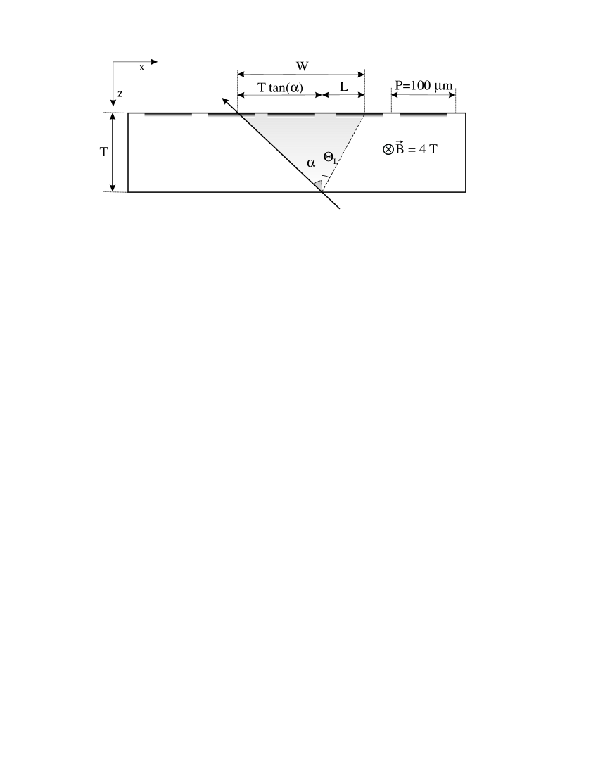
To reconstruct hits pixels with charge above 2000 electrons were selected and clusters were formed by adjacent pixels above threshold. Both side and corner adjacent pixels were included in the cluster. In addition, clusters adjacent to the matrix border were excluded. Figure 2 shows the definition of the track impact angle with respect to the sensor plane along the direction. The track is orthogonal to the sensor plane along the axis orthogonal to . The magnetic field produces a Lorentz shift towards the right direction. Thus, the total charge width is given by
| (1) |
The cluster is projected along the axis by summing the charge collected in the pixels with the same coordinate. If the cluster is given by a single pixel its position is given by the pixel center. For larger clusters the hit position is calculated with a center-of-gravity algorithm.
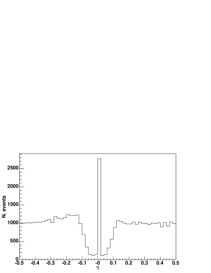
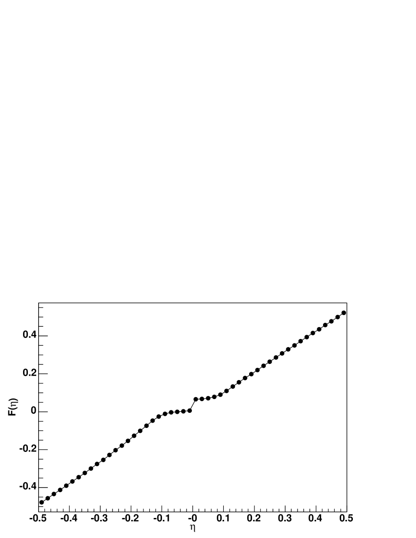
To further improve the spatial resolution for events in which charge is shared among several pixels the so-called -correction is introduced [9]. As we will discuss, the correction is particularly effective on irradiated devices, where the effects of inhomogeneous charge collection are larger. Assuming that the number of particles crossing the sensor is uniformely distributed along we should expect the reconstructed position within a pixel to be uniformely distributed. We define as the non-integer part of the reconstructed position. Figure 3 shows the distribution of for all events, where corresponds to the center of the pixel cell and to the borders. The measured distribution is almost flat in the pixel regions closer to the pixel borders and it shows a dip at the center. The peak at is due to single pixel clusters. For each we associate a corrected value given by the function
| (2) |
where is in pixel units. The function is shown in Fig. 3. The corrected position is calculated by adding to the integer part of the reconstructed position.
4 Cluster size and position resolution
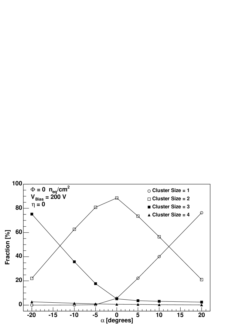
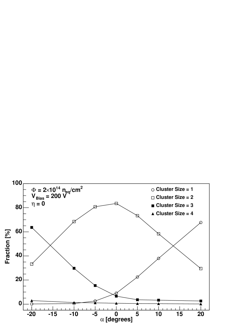
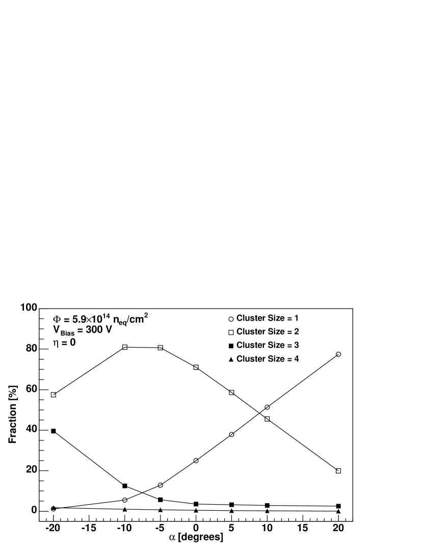
Figure 4 shows the fraction of events for different cluster sizes as function of the impact angle and for different irradiation fluences. At negative angles the Lorentz shift and the geometrical sharing term sum up giving large values. For perpendicular tracks () the total charge width is given by the Lorentz shift and then decreases for . Clusters are larger than one pixel in the majority of cases, however at high irradiation fluences the higher bias voltage produces a narrower Lorentz deflection and, consequently, a smaller cluster size.
The combination of carrier trapping and higher bias voltage produces smaller cluster sizes after heavy irradiation. The average cluster size for an unirradiated detector with Vbias=200 V and perpendicular tracks is 2.0. After a fluence of neq/cm2 and Vbias=300 V the value is 1.8.
The position resolution was estimated by comparing the hit position, , reconstructed as described in Section 3 with the true impact position, , generated by the simulation. The residuals were defined as and the position resolution was given by the width of a Gaussian fit of the residual distribution. The position resolution for tracks perpendicular to the sensor is summarized in Table 1 for clusters of two pixels. The position resolution for all events is shown in the last column, where the position of the two-pixels clusters was corrected. The simulation shows that position resolution below 15 m can be achieved even after heavy irradiation. In addition, the precision can be improved by correcting the reconstructed position as described in Section 3.
| Vbias | Resolution | Resolution | Total Resolution | |
|---|---|---|---|---|
| (neq/cm2) | (V) | w/o corr. (m) | (m) | (m) |
| 0 | 200 | 9.30.1 | 9.10.1 | 9.00.1 |
| 2 | 200 | 13.40.2 | 11.90.2 | 12.10.2 |
| 6 | 300 | 13.30.1 | 12.30.1 | 12.90.1 |
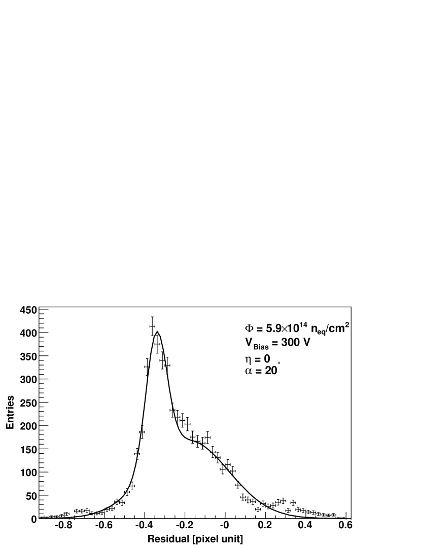
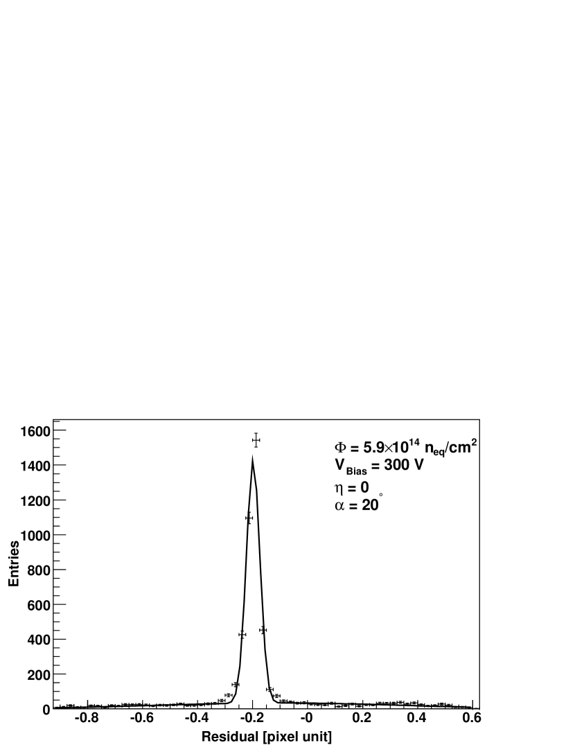
The size of the corrections become particularly significant after irradiation and for narrow charge widths. Figure 5 shows the residuals distribution for clusters of two pixels, simulated for a sensor irradiated to neq/cm2 and for tracks with . The distribution before correction (Fig. 5) is not described by a single Gaussian and is affected by large systematic errors which depend on the interpixel hit position. The distribution in Fig. 5 shows that the systematic errors can be largely reduced by applying the -correction.
5 Conclusions
In this paper a detailed simulation of the silicon pixel sensors for the CMS tracker was used to estimate the effects of radiation damage on the position resolution. The simulation, incorporating a double junction model of radiation damage and trapping of charge carriers, provides a good description of the charge collection measurements in the fluence range from neq/cm2 to neq/cm2.
The simulation shows that a position resolution below 15 m can be achieved for perpendicular tracks in the CMS trasverse plane even after heavy irradiation. In addition, we show that the position resolution can be improved by applying corrections.
References
- [1] CMS: The Tracker Project, Technical Design Report, CERN/LHCC 98-6. CERN, Switzerland.
- [2] V. Chiochia, et al., Simulation of heavily irradiated silicon pixel sensors and comparison with test beam measurements, IEEE Trans. Nucl. Sci. 52 (2005) 1067–1075.
- [3] A. Dorokhov, et al., Electric field measurement in heavily irradiated pixel sensors. Presented at the 13th International Workshop on Vertex Detectors for High Energy Physics, Menaggio, Italy, 13-18 September 2004. Submitted to Nucl. Instrum. Meth. eprint [physics/0412036].
- [4] V. Chiochia, et al., A double junction model of irradiated silicon pixel sensors for LHC, presented at the 10th European Symposium on Semiconductor Detectors, June 12-16 2005, Wildbad-Kreuth, Germany. Submitted for publication in Nucl. Instrum. Meth., eprint [physics/0506228].
- [5] M. Swartz, et al., Observation, modeling, and temperature dependence of doubly peaked electric fields in irradiated silicon pixel sensors, presented at the Int. Workshop on Semiconductor Pixel Detectors for Particles and Imaging, September 5-8 2005, Bonn, Germany. Submitted for publication in Nucl. Instrum. Meth., eprint [physics/0510040].
- [6] M. Swartz, CMS pixel simulations, Nucl. Instrum. Meth. A511 (2003) 88–91.
-
[7]
M. Swartz, A detailed simulation of the CMS pixel sensor, CMS Note
2002/027, July 2002.Available online:
http://cmsdoc.cern.ch/doc/notes/doc/NOTE2002_027. - [8] Synopsys Inc., Mountain View CA (USA), TCAD 9.0 User’s Manual, http://www.synopsys.com.
- [9] E. Belau, et al., The charge collection in silicon strip detectors, Nucl. Instr. Meth. 214 (1983) 253.