Robustness of One-Dimensional Photonic Bandgaps Under Random Variations of Geometrical Parameters
Abstract
The supercell method is used to study the variation of the photonic bandgaps in one-dimensional photonic crystals under random perturbations to thicknesses of the layers. The results of both plane wave and analytical band structure and density of states calculations are presented along with the transmission coefficient as the level of randomness and the supercell size is increased. It is found that higher bandgaps disappear first as the randomness is gradually increased. The lowest bandgap is found to persist up to a randomness level of percent.
pacs:
(350.3950) Micro-optics.I Introduction
Since the pioneering work of E. Yablonovitch Yablonovitch and S. John John , research on photonic crystals(PCs) has enjoyed a nearly exponential increase. The manufacture of PCs at the optical regime has become a reality lin . Manufacturing brings with it the practical reality of random errors introduced during the manufacturing process and it is the effect of these random errors on the desirable features of PCs, namely photonic band gaps, that we wish to address in this paper.
Bandgaps in PCs depend on two crucial properties: an infinite and perfect translational symmetry. Clearly, in real life no crystal is infinite in size or perfectly periodic. When randomness is introduced in the geometry of the PC, one quantity of interest is the size of the bandgaps as the level of randomness is increased, and whether the bandgaps of the bulk perfect PC will survive the randomness. Same considerations apply for a finite PC. In fact, even for a perfect but finite PC, one needs to give up the notion of a bandgap and has to be content with severe depressions in transmittance instead. In this paper, we will consider both finite imperfect PCs by examining the dependence of their transmittance on randomness, and bulk imperfect PCs by determining their density of states (DoS) under varying degrees of randomness, using the supercell method.
Although much has been done lizhang2000 ; lizhangzhang2000 ; fanville95 ; sigalas ; kaliteevski2000 regarding imperfect two- and three-dimensional PCs, we feel that a study of the problem for one-dimensional PCs is warranted because of the inherent simplicity of the geometry and because a variety of extremely accurate mathematical tools are readily available which allow a detailed study of the problem without having to compromise accuracy. For instance, because the electric field and its first derivative are continuous across the interface, and because of the low dimensionality of the PC, the convergence problem that plagued band structure calculations for many 3D PCs sozuer ; moroz is essentially non-existent for 1D structures. Thus, we were able to use the old trusted plane wave (PW) method to find the band structure and the DoS for supercell sizes not even imaginable in three- or even two-dimensional supercell calculations lizhang2000 ; lizhangzhang2000 . One can obtain better than 0.1% convergence with as few as 30 plane waves per unit cell in the supercell. The transmission coefficient, too, can be calculated for nearly arbitrary supercell sizes. Finally, one can calculate the band structure and the imaginary part of the wave vector using a semi-analytical approach for very large supercells.
The 1D PC is, in many ways, the “infinite square-well” problem of photonic crystals. It contains the essential features of its bigger cousins in two and three dimensions without the mathematical complexities and the accompanying numerical uncertainties sozuer ; moroz that can sometimes overshadow the essentials. For example, with 3D face centered cubic structures, it becomes practically impossible, due to convergence problems, to increase the supercell size beyond (or at most ) conventional cubic unit cells which contain only 32 primitive cells per supercell (or 108), since typically at least terms per primitive cell are necessary to ensure sufficient convergence for inverse opal structures. It’s not obvious from the start whether a randomness analysis with such small supercell sizes would yield results that are physically meaningful. Artifacts due to the small supercell size are bound to be inextricably intertwined with the physically significant bulk features of the imperfect PC. It’s important to realize that, with the supercell method one still calculates the bands of an infinite perfect PC. The randomness is only within the supercell, but on a global scale, it’s still a perfectly periodic structure! In order to be able to resolve the supercell artifacts from the physical features brought about by randomness, one needs to ensure that the interaction between neighboring supercells, which, to a good approximation, is proportional to the surface area of the supercell, be small compared to the bulk properties of the imperfect PC, which can be taken to be proportional to the volume of the supercell. Hence, on purely dimensional grounds, one can argue that the surface to volume ratio of the supercell , where is the linear size of the supercell, should be small compared to the typical length scale of the problem, namely the wavelength of the bandgap. We allowed the supercell size to vary from to , and one can clearly see the supercell artifacts gradually diminishing while the bulk features become more prominent in the limit as . On the other hand, 1D structures can have features, such as a bandgap for any geometry and any refractive index contrast, that are certainly not shared by 2D or 3D PCs.
The precise distribution of randomness in the geometry of a PC would surely depend on the details of the specific manufacturing process. In the interest of simplicity, we chose the simplest distribution, the uniform distribution, in our study. As the unit cell, we chose a unit “supercell” that consisted of up to unit cells. The thicknesses of the layers were perturbed by a given percent, by adding random numbers chosen from a uniform distribution. As the unperturbed structure, we chose the quarter-wave stack that has, for a given dielectric contrast, the largest relative gap between the first and the second bands, as can be seen in Fig. 1. In what follows, we will consider this structure with a dielectric contrast of 13 as our perfect PC.

For 1D PCs, one further has the luxury of calculating the bandgaps using an analytical methodyeh . This approach also permits the calculation of the imaginary part of the wave vector in the forbidden gap region and allows a reliable assessment of the accuracy of the plane wave method for the problem at hand.
We also investigated the transmission coefficient for a unit cell quarter-wave stack structure. The transmission coefficient was calculated by simply matching the boundary conditions for the electric and the magnetic fields at each interface between the slabs in the multilayer structure.
II Density of states calculation with the PW method
Maxwell’s equations for waves propagating in the direction in a medium with a dielectric constant that depends only on , can be reduced to
| (1) |
where is parallel to the slabs. With periodic along with lattice constant , and translationally invariant along and ,
where , is a reciprocal lattice vector with , and can be written as
| (2) |
where . For a given , this yields an -dimensional generalized eigenproblem
| (3) |
or by multiplying both sides from the left by , one obtains the ordinary eigenproblem
| (4) |
where , , and is the inverse of the matrix . For a given value of , a truncation of this -dimensional ordinary eigenvalue problem yields, by retaining only the -vectors with , the band structure and the modes . We choose a structure where the dielectric constant alternates between two values and each with thickness and , respectively.
The choice of the lattice constant is not unique. Although the choice is the most obvious and the most convenient, the lattice constant can be chosen as any integer multiple of , . With a choice for with , and following the same formalism one can write
and
where , with and . Clearly, to get results with the same level of accuracy as before, i.e. with , one would now need to include times as many plane waves in the expansion, which simply increases the computational burden, both in terms of storage and computing time.

The band structure for and are displayed in Fig 2 for a perfect PC. i The folding of the bands in the first Brilloin zone for each , makes the appearance of the bands rather different for each case, although the DoS and the eigenfunctions would be independent of the choice of the supercell size. The frequency is plotted in units of for all cases, so the frequency scale is not affected with the result that the bandgaps are at the same frequency, as would be expected. To calculate the DoS, we choose a uniform mesh in -space to calculate the bands and then choose a small frequency window, , and count the number of modes whose frequencies fall within that window.
We add random perturbations to the thicknesses of the layers in the supercell such that
| (5) |
where are the unperturbed values of the thicknesses of the layers, i.e. the quarter-wave stack values, is a uniformly distributed random number in the interval . We control the amount of disorder by varying the percent randomness parameter between 0 and 1. corresponds to perfectly periodic structures, and corresponds to fluctuation where , can range between and twice their unperturbed values. When disorder is introduced, gaps appear between every fold for .

In Fig. 3 we plot the upper and lower limits for the lowest three bandgaps as a function of , the percent randomness with a supercell size of . Note that since for quarter-wave stack structures the even numbered gaps are closed, the bandgaps in this figure are in fact the first, third and the fifth bandgaps of a 1D PC with arbitrary values for the layer thicknesses. The third gap centered at closes around , the second gap centered at closes around , and the lowest gap centered at closes around . The ratios of the critical values of randomness agree well with the ratios of the corresponding center gap frequencies, . This can be understood using the simple argument that when the random fluctuations in the thicknesses of the layers become comparable to the wavelength of the gap center, the bandgap disappears since the destructive interference responsible for the existence of the forbidden band depends on the long range periodicity at that scale.
II.1 Analytical Method


As discussed in detail in Refyeh , for dielectric layers with thicknesses , with dieletric constants , for a given , one can obtain the transfer matrix, defined by
| (6) |
where
| (7) |
with
Imposing the Bloch condition on the -field, one obtains,
| (8) |
Comparing with Eq. 6, the eigenvalues of the transfer matrix are seen to be . Then, for , is real and is given by , while for , is complex with and . is the decay length of the evanescent mode, and is a measure of the strength of the bandgap. For finite PCs, it’s desirable to have to have a significant drop in transmittance. The advantage of the exact method is that the supercell size can be increased to values that are practically impossible using the PW method. While with the PW method, using 30 plane waves per unit cell of the supercell, the memory requirements scale as , and the time requirements scale as , the exact method requires a very small amount of memory.
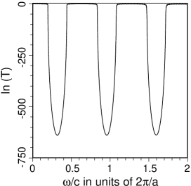
The only disadvantage of the analytical method over the PW method is that, while in the PW method one chooses a real and calculates the frequencies corresponding to that value of , in the analytical method, one chooses the frequency and calculates the real and imaginary parts of , and , corresponding to that value of . If the bands are nearly flat, as is the case for very large supercell sizes, then one needs to sample the frequency interval of interest in very tiny increments in in order to “catch” a propagating mode. Thus the computation time can become very large. Also for large values of , the transfer matrix can have very large elements so one requires very high precision in order to calculate the transmission resonance frequencies. We used quadruple precision (128-bit) floating point variables and functions in the Intel Fortran compiler in order to be able to resolve the transmission resonances for supercell sizes up to . For large values of , even 128-bit precision is not sufficient, with the result that cannot be made to completely vanish due to insufficient precision. Nevertheless, the propagating modes appear as sharp cusps in the vs graph which can easily be identified (Fig. 4). For , one needs more than 128-bit precision to even see the cusps in (Fig. 4). For larger values of , we used Mathematica for its arbitrary precision capabilities. However, compared to compiled code, Mathematica is slower by several orders of magnitude, so we had to stop at around .

To understand the bulk features of imperfect PCs using the supercell method, one would need a large supercell, in fact the larger the better. As the supercell size is increased, small bandgaps begin to appear over regions that used to have propagating modes. One would normally expect the gaps of the perfect crystal to gradually shrink in size, rather than have more gaps, so this result seems somewhat puzzling at first sight. However, as the supercell size is increased, the statistical fluctuations decrease, and the pass bands become increasingly more densely populated. In Fig 4 we display the behavior of as is increased. As becomes larger what used to be a photonic bandgap becomes more and more populated with transmission resonances, and the forbidden gap edges gradually approach each other, narrowing the gap. It’s possible that as , the whole bandgap region will be populated, albeit extremely sparsely, and instead of the bandgap, we will have a region where the DoS is extremely small—but non-zero nevertheless. We were able to increase up to and the bandgap was reduced as became larger, although the decrease for very large values was very small. To actually see the gap narrow even more would require an impractically large .


The number of transmission resonances in any fixed frequency interval is proportional to , so in the bulk limit with , any wave packet with a small, but nonzero frequency spread would contain many transmission resonances and thus would be partly transmitted and partly reflected. Clearly in the bandgap regions of the perfect PC, the density of these transmission resonances is extremely small, and these regions still appear to be bandgaps with a large, but still finite, supercell. Hence, it seems plausible to conclude that one cannot speak of a “true bandgap” for imperfect PCs, but only of large depressions in the DoS, which, in practice, would serve the same purpose as bona fide bandgaps. For instance, for a cavity made of an “impurity” embedded in a PC, localized cavity modes would eventually leak out through the PC “walls” of finite thickness, regardless of how perfect the PC walls are, bacause of the finite thickness of the walls. For such an application, what is important is that the lifetime of the cavity mode be much larger than the relevant time scale. Since the lifetime of the cavity mode is a function of the transmittance, for a given value of transmittance, one would simply need to use thicker walls as the random perturbations are increased.
II.2 Transmittance


Practical applications must necessarily use finite sized PCs, and for such structures, a quantity of more relevance is the transmittance. We calculate the transmittance by considering a PC of unit cells, and each layer is perturbed as described earlier. The transmission coefficient is calculated by imposing the boundary conditions for , , and at each layer boundary (Figure 5). This yields a set of linear equations for the unknowns . Setting the incident field , and assuming vacuum dielectric values for the incident and transmitted fields, , one obtains, and for the reflection and transmission coefficients, respectively. Alternatively, one could also obtain and from the transfer matrix as detailed in Ref. yeh but with our approach, we can also obtain the within each layer. For a given frequency in the gap region, the dependence of on the number of layers is approximately linear for all values of the randomness parameter , as is the case yeh for the perfectly periodic finite crystal (Fig. 6). However, depending on the level of randomness can change by many orders of magnitude. In practice, this would mean that in order to obtain a given value of transmittance using an imperfect PC, one would now have to use a thicker PC.
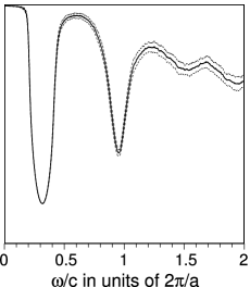
Although there is a strong relationship between the transmittance of a finite imperfect PC, and the modes of the superlattice formed by choosing the same exact finite PC as the unit supercell, this relationship is not perfect in the sense that the existence of a propagating mode does not necessarily imply a large value for . Conversely, the existence of a bandgap does not necessarily imply a low value for the transmittance . A close examination of the and vs plots in Fig 7 will reveal that, on a large scale, the transmission has a dip where is large, and when is small the transmittance is nearly unity. However, a closer look at a finer scale in Fig. 7, one sees that can still be not as large as what one might expect from .
Looking at the plots of vs Fig. 7, one could argue that sets an upper limit for . This upper limit seems to be a linearly decreasing function of . That the actual value of can fluctuate below a particular value for a given can be understood if one considers the coupling of the incident plane wave to the modes inside the PC. If, owing to the randomness, the propagating mode happens to have a small amplitude near , it will not be transmitted effectively. Similar coupling problems were reported by Robertson et al meade for 2D PCs.
III Conclusion
We studied the behavior of the photonic band gap and the transmittance for an imperfect PC using the supercell method combined with both the plane wave method and the analytical method. We also studied the transmittance for an imperfect finite 1D photonic crystal and have shown that the results we obtain in all cases are consistent. The bandgaps of the perfect PC are replaced by a DoS that is extremely small to be detected even with extremely large supercells that consist of over 32000 unit cells. The higher frequency bandgaps disappear first with the lowest gap closing at around a randomness level of .
IV Acknowledgements
This work was supported by a grant from the Research Fund at Izmir Institute of Technology. The band structure computations were performed on the 128-node Beowulf cluster at TUBITAK, the Scientific and Technological Research Council of Turkey.
References
- (1) E. Yablonovitch, Phys. Rev. Lett. 58, 2059 (1987).
- (2) S. John, Phys. Rev. Lett. 58, 2486 (1987).
- (3) S.Y. Lin, J.G. Fleming, D.L. Hetherington, B.K. Smith, R. Biswas, K.M. Ho, M.M. Sigalas, W. Zubrzycki, S.R. Kurtz, and J. Bur, Nature (London) 394, 251 (1998).
- (4) Pochi Yeh, “Optical Waves in Layered Media” John Wiley & Sons, (1988).
- (5) H.S. Sözüer, J.W. Haus, and R. Inguva, Phys. Rev. B45, 13962 (1992).
- (6) A. Moroz, Phys. Rev. B66, 115109 (2002).
- (7) Z.Y. Li and Z.Q. Zhang, Phys. Rev. B62, 1516 (2000).
- (8) Z.Y. Li, X. Zhang and Z.Q. Zhang, Phys. Rev. B61, 15738 (2000).
- (9) S. Fan, P. R. Villeneuve, and J.D. Joannopoulos, J. Appl. Phys. 78, 1415 (1995).
- (10) M. M. Sigalas, C. M. Soukoulis, C. T. Chan, R. Biswas, and K. M. Ho, Phys. Rev. B 59, 12 767 (1999).
- (11) M.A. Kaliteevski, J.M. Martinez, D. Cassagne, and J.P. Albert, Phys. Rev. B66, 113101 (2002); A.A. Asatryan, P.A. Robinson, L.C. Botten, R.C. McPhedran, N.A. Nicorovici, and C. MartijndeSterke, Phys. Rev. E 62, 5711 (2000).
- (12) W. M. Robertson, G. Arjavalingam, R. D. Meade, K. D. Brommer, A. M. Rappe, and J. D. Joannopoulos, Phys. Rev. Lett. 68, 2023 (1992).