Light-Weight Base Station Antenna with Artificial Wire Medium Lens
P.O. Box 3000, FI-02015 TKK, Finland
2Dept. Physics, State University of Informational Technology,
Mechanics and Optics at St. Petersburg,
Sablinskaya 14, 197101, St. Petersburg, Russia)
Address for correspondence:
Pekka Ikonen,
Radio Laboratory, Helsinki University of
Technology,
P.O. Box 3000, FI-02015 TKK, Finland.
Fax: +358-9-451-2152
E-mail: pikonen@cc.hut.fi
Abstract
In this paper we study the possibility of utilizing a loaded wire medium as an artificial material for beam shaping element in base station antenna applications. The wires in the lattice are loaded with a proper capacitive impedance to come up with a structure effectively operating as a dielectric lens at the UMTS (Universal Mobile Telecommunications System) frequency range. It is proven with full-wave simulations that the interpretation of a finite size wire lattice as a dielectric lens is physically sound even with a moderate number of lattice periods. A prototype having a mechanically reconfigurable beam width is constructed and measured. It is shown that very promising performance can be achieved with a rather simple structure and a cheap manufacturing process.
Key words: Wire medium, artificial dielectrics, lens antenna
1 Introduction
It is expected that the enormous growth of the traffic load in the wireless networks will continue in the near future. The transition era from the 3rd generation systems to 4G networks leads to applications that will require huge data rates and therefore extremely efficient network planning [1, 2]. Undoubtedly, novel implementation techniques are needed to lighten the pressure concerning the improvement of base station antennas. Ultimately, the antenna must be robust and cheap for mass production implying that the structure should be small and simple. However, sectorized cells and the natural evolutional stages of the network often set the demand for the antenna to operate in different modes with different service areas. Therefore, the antenna should offer a possibility for a tunable beam width or a switchable beam direction. Incorporating intelligence in a miniaturized and simple antenna structure while still maintaining the efficiency high, is not an easy task.
The operational principle of a medium consisting of periodically arranged wires has been known for a long time [3, 4]. This kind of wire medium (also called rodded medium) is known to operate as an artificial dielectric with negative effective permittivity at low frequencies. Due to the periodic nature of the wire medium, the medium can be considered as an electromagnetic band-gap (EBG) structure introducing frequency bands in which electromagnetic waves cannot propagate [5]. A detailed analysis of the electromagnetic band structures of the wire medium can be found e.g. in [6, 7]. The transmission and absorption properties of a two-dimensional (2D) lattice of conducting cylinders have been presented [8], and the effective electronic response of a system of metallic cylinders has been introduced [9].
The nature of wave propagation inside the wire medium and its dispersion properties have also been subjects of comprehensive studies. In [10] the wave propagation inside the wire medium was studied in detail. Comprehensive analytical study of the dispersion and reflection properties of the wire medium can be found e.g. in [11, 12, 13]. Authors of [12] considered also a wire medium periodically loaded with bulk reactances and presented the dispersion relation for this kind of loaded wire medium. A quasi-static model for the loaded wire medium can be found in [14].
Recently, extensive research has been devoted to the utilization of the wire medium in microwave applications. The transmission properties of loaded and unloaded wire medium have been theoretically and experimentally analyzed in [15]. In [16] the authors presented an EBG structure consisting of cut metal strips mounted with pin-diodes. Depending on the diode biasing the structure was shown to prohibit the propagation of the electromagnetic waves or to create a very directed beam for a planar antenna. Discussion about the performance of antennas inside wire lattices has been presented in [17], and authors of [18] presented an experimental demonstration for the radiation characteristics of a conventional dipole inside the wire medium. The utilization of dipole arrays (somewhat resembling the case of cut wires with the introduced cap width extending towards infinity) as a beam shaping lens was introduced in the beginning of 80’s by Milne [19]. A mathematical design procedure for a non-homogenous wire medium lens antenna can be found in [20]. Analytical and numerical results for the radiation properties of a simple radiator in the vicinity of the loaded wire medium were presented in [21], and an experimental demonstration of the feasibility to use the loaded wire medium with compact and directive antenna applications can be found in [22].
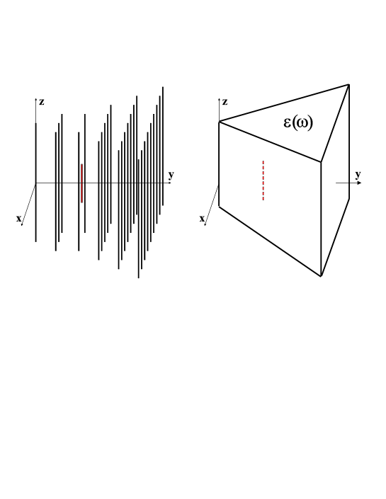
In the present paper we utilize the properties of the loaded wire medium [12, 21] to design a compact dual-mode base station antenna having a mechanically reconfigurable beam width. After capacitive loading the plasmon-like band-gap inherent to the conventional wire medium disappears and the structure becomes transparent for radiation [12, 15]. Moreover, the proper loading allows us to reduce dramatically the size of the radiator without a loss of the radiation efficiency [21]. It is shown below that the interpretation of the loaded wire medium as an artificial dielectric lens is possible even with a moderate number of lattice periods. Around the frequency range of interest the wire lattice operates as a finite size block of artificial dielectric as schematically depicted in Fig. 1. The key benefits of the proposed antenna structure are low cost, cheap manufacturing process, and extremely light weight. An antenna prototype is manufactured and measured. It is shown that the theory of an aperture radiator is applicable in the designing process of the wire medium lens antenna.
2 Loaded wire medium: Revision of the dispersion properties
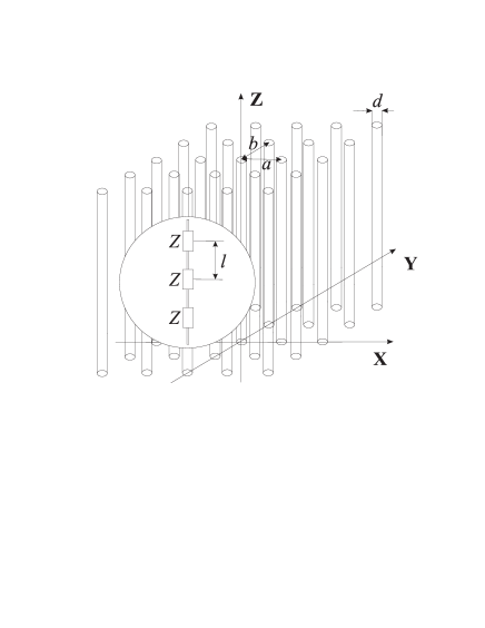
A schematic illustration of the loaded wire medium is shown in Fig. 2. It is known that the conventional wire medium (solid wires) exhibits a plasmon-like band-gap starting from zero frequency [7, 12, 15]. This means that at low frequencies electromagnetic waves cannot propagate through the wire medium (except to the direction along the wires). This further implies that if a radiator is brought inside conventional wire medium, a channel must be configured in the structure to permit the emission of electromagnetic waves (see e.g. [18] for experimental demonstration). In addition to this, the transversal size of such a structure is necessarily rather large due to destructive interaction between the source current and the currents flowing in the closely located solid wires. When the wires are loaded with bulk capacitances the low frequency band-gap disappears [12, 15]. Moreover, it was analytically shown in [21], and experimentally proven in [22] that the problem of field cancelation can also be overcome with the use of bulk capacitances.
Let us consider the loaded wire medium periodically loaded with bulk capacitances as shown in Fig. 2 ( = ). In [12] the dispersion equation for such a medium was formulated in terms of Floquet harmonics, scattered by the set of parallel wire grids periodically located along the axis (with period , see Fig. 2). Authors of [12] presented also a simplified expression for the full dispersion equation applicable for dense wire lattices (the lattice periods and are much smaller than the wavelength in the matrix material). Moreover, special attention was devoted to waves traveling orthogonally to the wire axis (the -component of the propagation factor is zero, = 0). This special case was considered at low frequencies compared to the first lattice resonance of the loaded wire medium. At these frequencies the magnetic properties of the medium are negligible and the effective medium model becomes valid. With the aforementioned assumptions, the simplified dispersion equation for dense wire lattices was reformulated using the resonant effective permittivity
| (1) |
where and are the material parameters of the matrix material, and is the wave number in the matrix material. For a capacitively loaded wire medium the resonant effective permittivity takes the form [12]
| (2) |
where is the load capacitance multiplied by the period of insertions , and is a geometrical parameter defined below. The resonant frequency can be expressed as [12]
| (3) |
where and are the lattice periods, and is the diameter of the wires. is defined as
| (4) |
The real part of the effective permittivity of a wire medium effectively loaded with a certain capacitance per unit length is shown in Fig. 3. We can see from Fig. 3 that the permittivity obeys the Lorenzian type dispersion rule. Before the first stop band ( 9.85 GHz) the refractive index is a monotonically growing function and the loaded wire medium operates as a usual artificial dielectric. At frequencies 9.85 13.7 GHz the medium can be considered as an artificial plasma (Re 0).
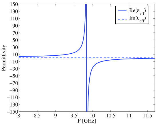
Relatively far away from the structure resonance the effective permittivity has nearly a constant value. For reference, around 2 GHz the real part of the effective permittivity equals approximately 2.0. Rather low and frequency-independent value for the permittivity of the lens can be considered as an advantage for the lens design. The aforementioned supports the idea of utilizing the loaded wire medium as a light-weight artificial dielectric lens, as schematically depicted in Fig. 1.
Note that this principle of utilization is fundamentally different from the angular filtering techniques [23] introduced in the literature for different types of EBG structures [15, 16, 24, 25]. The known beam shaping methods utilize defects in the EBG structure to create a transmission peak inside the original stopband. It is known [23] that a slight local change in the crystal period leads to localized resonant modes, and can be used for the realization of devices radiating energy in a very narrow angular range. At frequencies lying inside the original band-gap of the crystal, discontinuous wires [16] or dielectric rods [24, 25] located in front of a low gain radiator can also be used as simple angular filters. One of the biggest disadvantages of this utilization technique is a very narrow operational bandwidth. We, on the contrary, propose the utilization of the EBG structure far below the first stopband and regard the loaded wire medium as a piece of a usual homogenous dielectric.
It is also worth noticing that due to very high signal power levels used in base stations (e.g. Kathrein [26] reports the maximum power per input to be 300 W for most of the products), active components cannot be used in the lens due to unavoidable intermodulation products leading to distorted frequency spectrum. Therefore we seek for a solution where the bulk capacitances are implemented without using active components.
3 Designing the novel antenna structure
3.1 Desired characteristics
The goal of the following antenna design procedure is to come up with a compact base station antenna structure having two modes corresponding to two beam widths in the H-plane (the plane orthogonal to the wires). The carrying idea is to design as simple and robust antenna as possible. The beam width is to be reconfigured mechanically to maintain the simplicity of the design, and to avoid problems caused by active components when using high signal power levels. The targeted radiation characteristics are presented below:
-
1.
Frequency range 1920 – 2170 MHz (UMTS FDD range)
-
2.
Maximum transversal size 15 cm111The size of the reflector excluded.
-
3.
Backward radiation as small as possible
-
4.
Half-power beam width in H-plane 65∘ / 85∘
Other important features for a design close to an end product are the E-plane beamwidth, E-plane side lobe level, the gain, and the longitudinal size of the structure. The main practical importance of the present work is the demonstration of the beam switching with the help of the artificial wire medium lens. However, to be assure for the feasibility of the structure in base station antenna applications, we will also introduce the radiation pattern in E-plane, and the simulated gain values. The optimization of the antenna matching, and the details in the actual mechanical switching procedure are not discussed in the present work.
The main parameters characterizing the feasibility of the antenna structure are the deviation in the input impedance, front-to-back ratio (FBR), robustness and the H-plane beamwidth. Ideally, the only changing parameter between the modes should be the H-plane beamwidth. The robustness refers to the fact that the radiation characteristics of the antenna should not change dramatically when the parameters of the structure (e.g. the lattice parameters , the value of the load capacitance ) are changed slightly. This is very important in the view of the manufacturing process. To maintain the design as simple as possible, we seek for a solution where the structure consists of two parts. Namely, the antenna has a fixed part and a removable part. The fixed part consists of the radiator accompanied with a possible reflector, whereas the removable part is formed by the wires located in front of the radiator. Fixing the radiator and the reflector sets an additional demand for the removable part. In addition to producing different beam widths, the removable part should not change strongly the input impedance seen at the antenna terminals. This ensures a reasonable matching level with both modes.
3.2 Numerical design

Suitable geometry for the prototype leading to the desired
performance was found with numerical simulations conducted with a
commercial method of moments (MoM) simulator FEKO
[27]. It was suggested in [21] and experimentally
proven in [22] that to achieve a zenithal radiation pattern
in the H-plane, the optimal number of loaded wires with a
half-wavelength dipole is approximately 20–30 and the shape of the
lattice is close to a triangular one. This estimation laid the basis
for the optimization process.
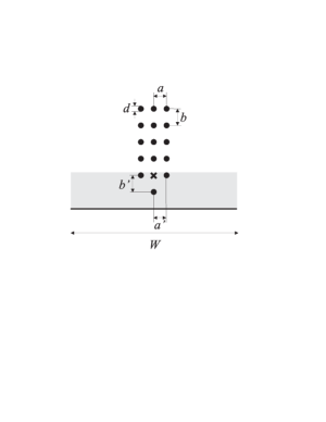
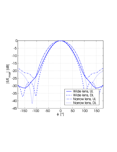
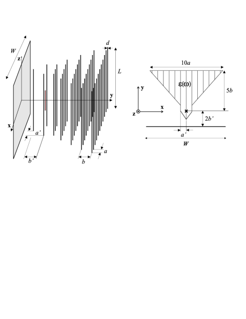
Fig. 4 shows the final outcome of the designing process. As we can see there is a considerable difference between the topology of the wide and the narrow lens. This is, however, well predictable according to the theory of an aperture radiator [28]: As the far field radiation pattern of an aperture radiator (e.g. a lens illuminated with a low gain radiator) is the Fourier transform of the illuminating field distribution, the wider is the aperture, the narrower is the beam. To suppress the backward radiation a metal reflector is used. The reflector can also be made of simple solid wires (with a distance between the wires much smaller than ) to lighten the wind load. The transversal size with the wide lens (excluding the reflector size) is 11.5 8.75 cm2 (0.77 0.60 ) implying that the structure is very compact. The transversal size of the structure with the narrow lens is 2.3 8.4 cm2 (0.15 0.55 ). The distance between the dipole and the closest wire is = 11.5 mm /13.
In the present design the beam switching (reconfiguration) function is implemented by manually changing the removable part in front of the radiator. Other possibilities (not studied in the present paper) could include fixing the lens topology and modifying the impedance loading by mechanically or electronically tuning the load capacitances. This, however, adds complexity to the design, and might require the use of active components in the lens.
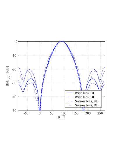
Fig. 5 introduces the simulated far field patterns in the H- and E-planes. The main simulated parameters are gathered in Table 1. Presented simulations have been conducted at the UMTS FDD uplink (UL) and downlink (DL) center frequencies, namely at 1.95 GHz and 2.14 GHz. As can be seen, the beam widths in the H-plane are very close to the goal values 65∘ and 85∘ with the wide and narrow lens respectively. The beam width in the E-plane is typical when using only one dipole as a source. The simulated gain values (at the center frequency = 2.045 GHz) with the wide and narrow lens are 10.9 and 9.6 dBi, respectively. A design closer to an end product could have e.g. a collinear array of crossed dipoles and a total height close to one meter. This would significantly narrow the E-plane beam width and increase the gain of the structure.
| Wide lens | |||||
|---|---|---|---|---|---|
| BW-3dB | FBR | Rrad | BW-3dB | FBR | Rrad |
| deg. | dB | deg. | dB | ||
| 66.5 | -30.2 | 63 | 64 | -29.6 | 115 |
| Narrow lens | |||||
| BW-3dB | FBR | Rrad | BW-3dB | FBR | Rrad |
| deg. | dB | deg. | dB | ||
| 82 | -18.5 | 64 | 85 | -20.1 | 90 |
3.3 Selected observations on the antenna behavior
In this section we have gathered some typical (qualitative) tendencies in the antenna behavior noticed during the the simulation process. One of the most important observations with the simulated structures (having a finite size reflector or no reflector at all) is the fact that a good FBR level contradicts rather heavily with a narrow beam width in H-plane. In other words, with nearly all the simulated lens topologies and reflector shapes, narrowing the H-plane beam width deteriorates the FBR (this can not readily be seen in the results presented for the prototype with two modes, since the whole lens topology is changed to manipulate the H-plane beam width). With a fixed topology of the lens (e.g. the wide lens topology in the prototype), the most effective way to narrow the H-plane beam width is to increase the value of the lattice parameter , see Fig. 4 for definition. This, however, has also a strong negative effect on the FBR level. If a rather moderate H-plane beam width is desired, the rows of wires can be brought in a close vicinity of each other still maintaining the FBR at a very good level [22]. If a considerably narrow H-plane beam width is to be achieved, the wave has to travel a longer distance in the lens (phase shifts of the currents induced to the wires far away from the radiator have to change rapidly enough). This means increasing the depth of the lens.
A general tendency with the simulated structures is that a good FBR level corresponds to a small value of the radiation resistance and vice versa. One of the biggest drawbacks of the studied structures is the strong deviation of the input impedance (radiation resistance) over the desired frequency range. Typically the change in the radiation resistance over the UMTS band is close to 50 percent, the minimum resistance occurring at lower frequencies. This naturally implies difficulties in maintaining the matching at a reasonable level over the whole frequency range, but also causes deviation in the beam width and FBR. With most of the studied structures the beam width is approximately 510∘ wider at the UL range than at the DL range (the aperture is narrower in terms of wavelength) and the deviation in the FBR is approximately 5 dB.
The value of the loading capacitance naturally depends on the insertion period of the loads. However, a suitable capacitance range producing reasonable performance can be found and the following observations can be made for this range (a fixed lens topology close to a triangular one assumed): Increasing the capacitance narrows the beam width but also deteriorates the FBR. This is due to the fact that with increasing capacitance the radiation resistance grows (up to a certain limit). When increasing the capacitance too much the radiation pattern changes very dramatically leading to a pattern with a very strong backward lobe and the main beam of a shape of a trefoil. On the other hand, a too low value for the capacitance leads to a structure that practically does not radiate (due to the destructive interaction between the source and the passive wires).
4 FDTD model for the dispersive dielectric lens
In this section we consider a finite size lattice of loaded wires as a block of dispersive dielectric material, as schematically depicted in Fig. 1. The dispersive behavior of the capacitively loaded wire medium has been shown to follow the expression (2) [12] (when the operational frequency is far below the first stop band and the array is dense). In this section we use an in-house finite-difference time-domain (FDTD) code and study the equivalence of the wire lattice to a dielectric lens in the case of a moderate number of lattice periods.
We choose to analyze the wide lens (for the transversal geometry see Fig. 4(a)). It was experimentally shown in [22] that the height of the structure (the dimension in the -direction) has only a very weak effect on the radiation pattern in the H-plane at low frequencies. Therefore to reduce the computational burden we consider without a significant loss of accuracy a two dimensional case in FDTD. The exact simulated structures are depicted in Fig. 6(a).
The dispersive behavior for the effective permittivity has been implemented in the code using the auxiliary differential equation (ADE) method [29]. The ADE method is applied for a medium having Lorentzian type dispersive permittivity with one pair of poles in its susceptibility response. For this kind of medium Ampere’s law can be expressed in time domain as
| (5) |
where is the value of the relative permittivity at infinite frequency, is the conductivity of metal parts in the medium and is the polarization current associated with the zeroth Lorentz pole pair. The evident generalization of (2) for the case of lossy media is
| (6) |
where is the static permittivity, is the undamped frequency of the zeroth pole pair (the undamped resonant frequency of the wire medium) and is the damping factor associated with (in the effective medium model (2) ). Utilizing (5) and (6) we construct a three step fully explicit procedure for updating the field components and the components of the polarization current.
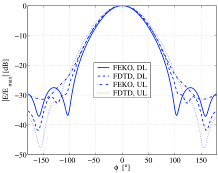
Fig. 6(b) shows the normalized far field patterns for the
electric field simulated with FEKO and FDTD. This figure
demonstrates the equivalence of the wire lattice to a finite size
dielectric block. The agreement between the shape of the main lobe
is good at both frequencies. The overall agreement of the two
patterns is good at the DL frequency. When thinking of dielectric
lenses implemented with substrates, the wire medium lens behaves in
a similar manner, however, it is cheaper and, more importantly,
lighter.
5 Prototype antenna
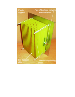
To manufacture the prototype we use a standard printed circuit board technique where the loaded wires are split strips on dielectric plates. The effects of the dielectric sheets have been taken into account by slightly modifying the prototype design, see Table 2. The modifications were enough to suppress the FBR with the cost of increased reflector size. Note, however, that the use of a larger size reflector is well justified since when mounting the antenna structure into a base station mast the mast itself operates as a large reflector.
| mm | mm | mm | mm | pF | pF | pF | mm | mm |
| 9.0 | 12.5 | 11.5 | 1.125 | 0.125 | 0.10 | 0.13 | 200 | 200 |
now and are the same for both lenses.
A photo showing the implemented prototype (with the wide lens connected) is presented in Fig. 7(a). FR-4 is used as the dielectric substrate material in the prototype antenna (the substrate thickness equals mm with the wide lens and mm with the narrow lens, ). The strip width is equal to mm with the wide lens and mm with the narrow lens. The period of the gaps (the insertion period of the loads) is equal to mm. To choose the gap width , the following approximate expression was used:
| (7) |
where the empirically found multiplication factor is approximately 0.7. One half-wavelength dipole was used as an active source. The dipole was fed with a coaxial cable having coaxial balun symmetrizing the feeding.
The measurements validating the main practical importance of the present work, the feasibility of the wire medium lens as a beam shaping element, are the measurement of the -parameter and the measurement of the 2D radiation pattern in the H-plane. These measurements confirm that the antenna matching does not change significantly when switching from one beam width to another, and that the beam width can be controlled by manipulating the lattice topology.
5.1 Matching level
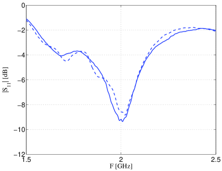
Fig. 7(b) shows the measured -parameter. The matching of the antenna has not been optimized (the best matching occurs a bit below the center frequency 2.045 GHz). A matching network (implemented e.g. using coaxial stubs) would improve the matching level at the center frequency and offer a possibility to tune the location of the -minimum. However, when thinking of a real end product, special attention should be devoted to the design of a wideband matching network.
With the introduced prototype the matching level remains almost the same for both wide and narrow lens. However, from the presented measurement we can not readily draw a general conclusion that the matching hardly depends on the removable part of the dielectric lens. This is due to the fact that the prototype antenna is only satisfactorily matched, with a well matched antenna the effect seen on the matching level can be larger.
5.2 2D radiation pattern
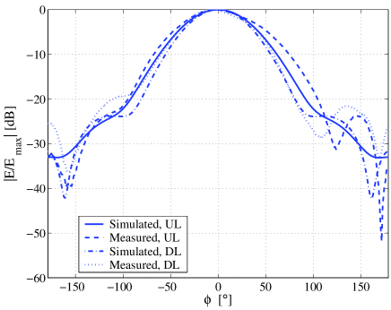
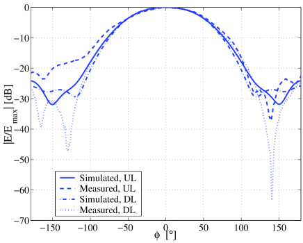
Fig. 8 introduces the measured H-plane radiation
patterns for both wide and narrow lenses. The FEKO
simulations for the implemented prototype are plotted for reference.
The measured half-power beam widths and FBRs are gathered in Table
3. The measured gain values (at the center frequency
= 2.045 GHz) with the wide and narrow lens are 9.8 and
8.0 dBi, respectively.
The measured results agree rather well with the simulated ones. The main lobe beam width and the FBR are in good agreement. The deviation is visible only in the side lobe directions. This deviation and the slight asymmetry of the pattern are, probably, caused by the feed network and the currents induced to the edges of the reflector plate. The reflectivity level of the measurement chamber was estimated to be 25 dB at 2 GHz (implying that the side and back lobe levels are in fact unreliable). The manufacturing process is fast, robust and inexpensive. However, a random discrepancy of approximately 10 percents in the load capacitance was measured over the slots with a high precision meter.
| Wide lens | |||
|---|---|---|---|
| BW-3dB | FBR | BW-3dB | FBR |
| deg. | dB | deg. | dB |
| 74 (66) | -33 (-33) | 62 (60) | -25.5 (-32) |
| Narrow lens | |||
| BW-3dB | FBR | BW-3dB | FBR |
| deg. | dB | deg. | dB |
| 90 (91) | -24 (-24) | 88 (92) | -26 (-26) |
† the value in the brackets is the simulated result.
6 Conclusion
In the present paper we have studied the applicability of the loaded wire medium as a beam shaping lens. The dispersion properties of the loaded wire medium introduced in the literature have been briefly revised. Contrary to the known EBG beam shaping techniques, we have chosen to utilize the frequency range far below the first stop band of the structure. In this region the loaded wire medium can be interpreted as a continuous artificial dielectric. A concept for a compact dual-mode base station antenna operating in the UMTS frequency range has been presented. We have confirmed that the theory of an aperture radiator is applicable when designing the wire medium lens antenna. A FDTD model for the dispersive dielectric lens having the wire lattice geometry has been constructed. The full wave simulations reveal that the loaded wire lattice operates as a dielectric block even with a rather small number of lattice periods. A promising performance of the prototype is shown to be achieved with a rather simple structure and cheap manufacturing process.
Acknowledgement
This work has been supported in part by Nokia Research Center, Filtronic LK, and TEKES.
References
- [1] W. Webb, The future of wireless communications, Boston: Artech House, 2001.
- [2] A. R. Mishra, Fundamentals of cellular network planning and optimization, New York: John Wiley Sons, 2004.
- [3] J. Brown, “Artificial dielectrics”, Progress in dielectrics, vol. 2, pp. 195–225, 1960.
- [4] W. Rotman, “Plasma simulation by artificial and parallel plate media,” IRE Trans. Ant. Propagat., vol. 10, pp. 82–95, 1962.
- [5] J. D. Joannopoulos, R. D. Mead, and J. N. Winn Photonic crystals: Molding the flow of light, Princeton University Press, Princeton, NJ, 1995.
- [6] V. Kuzmiak, A. A. Maradudin, and F. Pincemin, “Photonic band structures of two-dimentional systems containing metallic components,” Phys. Rev. B, vol. 50, no. 23, pp. 16835–16844, 1994.
- [7] N. A. Nicorovici, R. C. McPhedran, and L. C. Botten “Photonic band gaps for arrays of perfectly conducting cylinders,” Phys. Rev. E, vol. 52, no. 1, pp. 1135–1145, 1995.
- [8] M. M. Sigalas, C. T. Chan, K. M. Ho, and C. M. Soukoulis, “Metallic photonic band-gap materials,” Phys. Rev. B, vol. 52, no. 16, pp. 11744–11751, 1995.
- [9] J. M. Pitarke, F. J. García-Vidal, and J. B. Pendry, “Effective electronic response of a system of metallic cylinders,” Phys. Rev. B, vol. 57, no. 24, pp. 15261 -15266, 1998.
- [10] C. A. Moses and N. Engheta, “Electromagnetic wave propagation in the wire medium: A complex medium with long thin inclusions,” Wave Motion, vol. 34, pp. 301–317, 2001.
- [11] P. A. Belov and S. A. Tretyakov, “Dispersion and reflection properties of artificial media formed by regular lattices of ideally conducting wires”, J. Electromagnetic Waves and Applications, vol. 16, no. 8, pp. 1153–1170, 2002.
- [12] P. A. Belov, C. R. Simovski, and S. A. Tretyakov, “Two-dimensional electromagnetic crystals formed by reactively loaded wires,” Phys. Rev. E, vol. 66, 036610, 2002.
- [13] P. A. Belov, R. Marqués, S. I. Maslovski, I. S. Nefedov, M. Silveirinha , C. R. Simovski, and S. A. Tretyakov, “Strong spatial dispersion in wire media in the very large wavelength limit”, Phys. Rev. B, vol. 67, 113103, 2003.
- [14] S. I. Maslovski, S. A. Tretyakov, and P. A. Belov, “Wire media with negative effective permittivity: A quasi-static model,” Microwave Opt. Technol. Lett., vol. 35, no. 1, pp. 47–51, 2002.
- [15] J.–M. Lourtioz, A. de Lustrac, F. Gadot, S. Rowson, A. Chelnokov, T. Brillat, A. Ammouche, J. Danglot, O. Vanbésien, and D. Lippens “Toward controllable photonic crystals for centimeter- and millimeter-wave devices,” J. Lightwave Technol., vol. 17, no. 11, pp. 2025–2031, 1999.
- [16] A. de Lustrac, F. Gadot, E. Akmansoy, and T. Brillat, “High-directivity planar antenna using controllable photonic bandgap material at microwave frequencies,” Appl. Phys. Lett., vol. 78, no. 26, pp. 4196–4198, 2001.
- [17] G. Poilasne, J. Lenormand, P. Pouliguen, K. Mahdjoubi, C. Terret, and Ph. Gelin, “Theoretical study of interactions between antennas and metallic photonic bandgap materials,” Microwave Opt. Technol. Lett., vol. 15, no. 6, pp. 384–389, 1997.
- [18] G. Poilasne, P. Pouligen, K. Mahdjoubi, C. Terret, Ph. Gelin, and L. Desclos, “Experimental radiation pattern of dipole inside metallic photonic bandgap material,” Microwave Opt. Technol. Lett., vol. 22, no. 1, pp. 10–16, 1999.
- [19] R. Milne, “Dipole array lens antenna,” IEEE Trans. Antennas Propagat., vol. AP–30, no. 4, pp. 704–712, 1982.
- [20] M. G. M. V. Silveirinha, C. A. Fernandes, “Design of a non-homogeneous wire media lens using genetic algorithms”, Antennas and Propagation Society International Symposium, Columbus, Ohio USA, June 22–27, pp. 730–733, 2002.
- [21] C. R. Simovski and S. He, “Antennas based on modified metallic photonic bandgap structures consisting of capacitively loaded wires,” Microwave Opt. Technol. Lett., vol. 31, no. 3, pp. 214–221, 2001.
- [22] P. Ikonen, C. Simovski, and S. Tretyakov, “Compact directive antennas with a wire-medium artificial lens,” Microwave Opt. Technol. Lett., vol. 43, no. 6, pp. 467–469, 2004.
- [23] G. Tayeb and D. Maystre, “Rigorous theoretical study of finite-size two-dimensional photonic crystals doped by microcavities,” J. Optical Soc. America A, vol. 14, no. 12, pp. 3323–3332, 1997.
- [24] C. Cheype, C. Serier, M. Thévenot, T. Monédiére, A. Reineix, and B. Jecko, “An electromagnetic bandgap resonator antenna,” IEEE Trans. Antennas Propagat., vol. 50, no. 9, pp. 1285–1290, 2002.
- [25] B. Temelkuran, M. Bayindir, E. Ozbay, R. Biswas, M. M. Sigalas, G. Tuttle, and K. M. Ho, “Photonic crystal-based resonant antenna with a very high directivity,” J. Appl. Phys., vol. 87, no. 1, pp. 603–605, 2000.
-
[26]
The www–page of KATHREIN-Werke
http://www.kathrein.de -
[27]
The www–page of FEKO
http://www.feko.co.za/ - [28] C. A. Balanis, Antenna theory: Analysis and design, New York: John Wiley, 1997.
- [29] A. Taflove, Computational electrodynamics: The finite-difference time-domain method, Artech House, 1995.