Further author information: (Send correspondence to S.B.)
URL: http://www.zib.de/nano-optics/
S.B.: E-mail: burger@zib.de, Telephone: +49 30 84185 302
FEM Modelling of 3D Photonic Crystals and Photonic Crystal Waveguides
Abstract
We present a finite-element simulation tool for calculating light fields in 3D nano-optical devices. This allows to solve challenging problems on a standard personal computer. We present solutions to eigenvalue problems, like Bloch-type eigenvalues in photonic crystals and photonic crystal waveguides, and to scattering problems, like the transmission through finite photonic crystals.
The discretization is based on unstructured tetrahedral grids with an adaptive grid refinement controlled and steered by an error-estimator. As ansatz functions we use higher order, vectorial elements (Nedelec, edge elements). For a fast convergence of the solution we make use of advanced multi-grid algorithms adapted for the vectorial Maxwell’s equations.
keywords:
3D photonic crystals, photonic crystal waveguides, finite-element method, Maxwell’s equations, nano-optics1 Introduction
Photonic crystals (PhC’s) are structures composed of different optical transparent materials with a spatially periodic arrangement of the refractive index [1, 2]. Propagating light with a wavelength of the order of the periodicity length of the photonic crystal is significantly influenced by multiple interference effects. The most prominent effect is the opening of photonic bandgaps, in analogy to electronic bandgaps in semiconductor physics or atomic bandgaps in atom optics. Due to the fast progress in nano-fabrication technologies PhC’s can be manufactured with high accuracy. This allows for the miniaturization of optical components and a broad range of technological applications, like, e.g., in telecommunications [3]. The properties of light propagating in PhC’s are in general critically dependent on system parameters. Therefore, the design of photonic crystal devices calls for simulation tools with high accuracy, speed and reliability.
2 Light Propagation in Photonic Crystals
Light propagation in photonic crystals is governed by Maxwell’s equations with the assumption of vanishing densities of free charges and currents. The dielectric coefficient and the permeability are real, positive and periodic, , . Here is any elementary vector of the crystal lattice [2]. For given primitive lattice vectors , and the elementary cell is defined as A time-harmonic ansatz with frequency and magnetic field leads to an eigenvalue equation for with the constraint that is divergence-free:
| (1) |
Similar equations are found for the electric field :
| (2) |
The Bloch theorem applies for wave propagation in periodic media. Therefore we aim to find Bloch-type eigenmodes [2] to Equations (1), defined as
| (3) |
where the Bloch wavevector is chosen from the first Brillouin zone. A similar procedure yields the Bloch-type eigenmodes to Equations (2), however, in what follows we will concentrate on Equations (1).
In order to reformulate Equations (1) and (3) we define the following
functional spaces and sesquilinear forms:
(a) The set of Bloch periodic smooth functions is defined as
The Sobolev space is the closure of
with respect to the
-norm. The space is defined accordingly.
(b) The sesquilinear forms and
are defined as
| (4) | ||||
| (5) |
With this we get a weak formulation of Equations (1) and (3):
Problem 1
Find and such that
| (6) |
under the condition that
| (7) |
The space is the direct sum of the divergence-free subspace and the subspace of gradient fields , . Hence, can be decomposed as
(Helmholtz decomposition), where solves the equation
3 Finite Element Discretization
It is crucial to inherit the properties of the Helmholtz decomposition to the sub-spaces on the discrete level. Otherwise the discrete spectrum is polluted by many unphysical fields – called spurious modes – stemming from the space of gradient fields [4]. Using Nedelec’s edge elements to discretize the space and standard Lagrange elements of the same order to discretize the space gives a discrete counterpart to the Helmholtz decomposition and to the divergence condition [5].
We denote the discrete subspaces as follows: , . Bloch periodicity is enforced by a multiplication of basis functions associated with one of two corresponding periodic boundaries of the unit cell by the Bloch factor (see Equation (3)). All interior basis functions remain unchanged. An alternative approach is discussed by Dobson et al[6]: In this approach a wave equation is formulated for the periodic part of the magnetic field, (see Equation (3)). Modified finite element ansatz functions are constructed from the Sobolev space .
The discretized problem corresponding to Problem 1 reads as follows:
Problem 2
Find and such that
| (8) |
under the condition that
| (9) |
The finite element basis functions for are denoted by , the basis functions for by , . We expanding in ’s, . Inserting into Equation (8) yields the algebraic eigenvalue problem and the algebraic divergence condition
| (10) | |||||
| (11) |
with , and defined by . The matrix is hermitian, positive semidefinite and is hermitian, positive definite. In the algebraic form the Helmholtz decomposition reads as , where solves the algebraic problem
| (12) |
Due to the locality of the finite element basis functions all matrices are sparse.
4 Numerical solution of the eigenvalue equation
To solve the algebraic equation (10) we use a preconditioned Döhler’s method [7] which is based on minimizing the Rayleigh quotient. To avoid that the iteration tumbles into the non-physical kernel of the -operator we project the iterates onto the divergence-free subspace.
We use multi-level algorithms [8] for preconditioning as well for performing the Helmholtz decomposition (12). This is similar to the implementation by Hiptmair et al [9].
With this, the computational time and the memory requirements grow linearly with the number of unknowns [10]. Furthermore, we have implemented a residuum-based error estimator [11] and adaptive mesh refinement for the precise determination of localized modes (see chapter 6). As FE ansatz functions, we typically choose edge elements of quadratic order [4].
5 Band structures of 3D photonic crystals
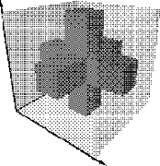
A model problem for 3D photonic crystals are so-called scaffold structures [12]. The geometry of a unit cell (sidelength ) of a simple cubic lattice is shown in Fig. 1. It consists of bars (width ) of a transparent material with relative permittivity and a background with (, : free space permittivity). For the calculation of the band structure the Bloch wavevector is varied along symmetry lines of the Brillouin zone (cf. Dobson [12]).
The band structure for light propagating in the scaffold structure is shown in Fig. 2a. It exhibits a complete bandgap around the reduced frequency of which is indicated by the dotted horizontal lines in Fig. 2a. Table 1 shows the four lowest eigenvalues at the -point() calculated on grids generated in 0, 1, resp. 2, uniform refinement steps from a coarse grid. In each uniform refinement step, every tetrahedron is subdivided into eight new tetrahedra. Shown are also the numbers of unknowns in the problem (number of ansatz functions in the finite element discretization) and typical computation times on a PC (Intel Pentium IV, 2.5 GHz). It can be seen that the computational effort grows linearly with the number of unknowns. Figure 2 (b) shows the dependence of the relative error of the four lowest eigenvalues () on the number of ansatz functions in the expansion of the eigenfunctions (number of unknowns). Here, is the eigenfrequency of the discrete solution with N unknowns, is the eigenfrequency of the quasi-exact solution obtained from a calculation on a finite-element grid with unknowns.
| Step | No DOF | CPU time [min] | ||||
|---|---|---|---|---|---|---|
| 0 | 3450 | 00:09.23 | 2.736e-01 | 2.740e-01 | 4.279e-01 | 4.288e-01 |
| 1 | 27572 | 01:46.33 | 2.730e-01 | 2.731e-01 | 4.266e-01 | 4.267e-01 |
| 2 | 220520 | 13:50.81 | 2.728e-01 | 2.728e-01 | 4.260e-01 | 4.260e-01 |
(a)
 (b)
(b)
(a)
 (b)
(b)
6 Calculation of defect modes using adaptive grid refinement
Light at a frequency inside the bandgap of a photonic crystal can be “trapped” inside defects of the structure [1]. This enables the construction of, e.g., waveguides (line defects) and micro-cavities (point defects).
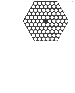
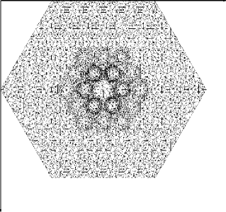
Figure 3 (a) shows the geometry of a 2D photonic crystal with a point defect (a missing pore in the center). It consists of a hexagonal lattice of air holes with a radius of in a material with a relative electric permittivity of . A corresponding coarse triangular FE grid is shown in Figure 3 (b). Please note that circular air pores are approximated by polygons. In the coarse grid shown in Figure 3 (a) the pores close to the center are approximated to a higher accuracy than pores in the outer regions. Obviously, when refining the coarse grid in order to get a discrete solution which is closer to the solution of Problem 1 in some norm, the best strategy will not be to refine the grid uniformly, but to refine it in certain regions onlz. For this adaptive grid refinement we have implemented a residuum-based error estimator [11].
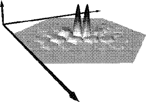
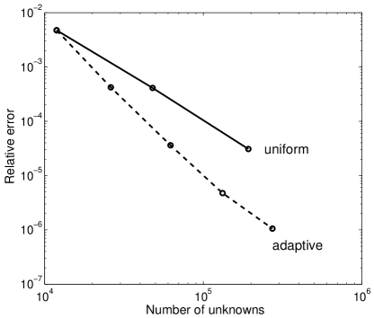
Figure 4 (a) shows the modulus of the magnetic field for the lowest-frequency trapped eigenmode, computed with adaptive refinement of the FE mesh. Figure 4 (b) shows the convergence of the eigenvalue corresponding to this solution towards the eigenvalue of a quasi-exact solution for adaptive grid refinement and for uniform grid refinement. Obviously, adaptive grid refinement is especially useful when the sought solutions are geometrically localized, or when the geometry exhibits sharp features, like discontinuities in the refractive index distribution. In this example, the use of the error estimator and adaptive refinement yields an order of magnitude in the accuracy of the error for a number of unknowns of .
7 Photonic crystal slab waveguide
Photonic crystal waveguides are promising candidates for a range of applications of micro- or nano-optical elements like dispersion compensators or input lines for further miniaturized elements. We examine a waveguiding structure composed of a slab waveguide (confinement of the light in z-direction by a high-index guiding layer) combined with a 2D hexagonal array of air holes (PhC) [13]. The waveguide is formed by a defect row of missing air holes in -K-direction. Therefore, in certain wavelength ranges, the light is confined vertically by total internal reflection in the guiding layer and horizontally by the photonic bandgap due to the 2D photonic crystal. We consider a guiding layer of height and refractive index with a substrate and superstrate of each and refractive index , and six rows of pores with refractive index on each side of the waveguide. These parameters correspond to the material system of air pores in a slab structure. The pore radius is , the lattice vectors have a length of nm.
Due to the symmetry of the problem it is sufficient to restrict the computational domain to one quarter of a unit cell. This reduced computational domain is shown in Figure 5(a). Here, the guiding layer is colored in dark gray, the substrate in gray, and the air pores in light gray. Mirror symmetries are applied to the upper plane (: center of the guiding layer) and on the left ( = 0). Periodic boundary conditions are applied to the front and back planes. At the left of the computational domain a W1 waveguide (i.e., width ) is formed by a missing row of air pores.
Fig. 5(b) shows some of the tetrahedral elements in the discretization of the geometry. A typical coarse grid for this problem consists of about tetrahedra.
Solving equation (10) for this problem on a PC (Intel Pentium IV, 2.5 MHz, 2Gbyte RAM) typically takes our FEM code a time of about 2 min and delivers the eigenvalue and the complex vector field for given Bloch wavevector . Figure 6 shows a specific guided mode in this structure. Part (a) of this figure shows the amplitude of the magnetic field in a gray scale representation. The plotted solution has been calculated for a Bloch wavevector of and corresponds to an eigenvalue of , which lies inside the first bandgap of the (2D) photonic crystal. As can be seen from the figure, the light field is localized in the high index guiding layer and in the region of the missing pore. White lines indicate equally spaced iso-intensity surfaces. Part (b) of the figure shows a cross-section through the same (vectorial) solution in the upper mirror plane (). In this plane the electric field vectors are oriented in the -plane, this solution corresponds to a TE-like mode.
8 Transmission through a finite photonic crystal
In order to simulate the transmission of an incident light field with a frequency through a photonic crystal of finite width we perform scattering calculations. In this case we have to seek a solution which fulfills Equation (1) resp. (2) for the given frequency on the computational domain with the following boundary condition: (a) the field on the boundary can be written as a superposition of incident and scattered light field: , (b) the scattered field is purely outgoing (radiation condition), which gives a condition for the outward normal derivative of , . We obtain a relation between and by using a modified type of perfectly matched layer boundary conditions, which also allows to treat certain types of inhomogeneous exterior domains [14].
In the following example we examine the light transmission through a finite 2D photonic crystal consisting of four rows of air pores in a high index material. Figure 7 shows the geometry of the problem: Air pores () of radius in a high-index material () form a finite hexagonal pattern. Periodic boundary conditions apply to two boundaries of the computational domain. Transparent boundary conditions to the exterior (which is assumed to be also filled by the high index material) are applied to the two other facets of the computational window. A plane wave with a freely chosen angle of incidence is incident onto one boundary. In order to measure the field transmission through the domain, the field on the opposing facet (BC t2) detected.
Figure 8 shows calculated field distributions for different frequencies of the incident plane wave ( deg). Each of these solutions has been calculated using adaptive mesh refinement, finite elements of quadratic order, and typically unknowns. The total calculation time on a standard laptop (Intel Pentium IV, 2.0 GHz) for each solution amounts about 10 sec. The fields in Figure 8 (a)-(j) correspond to decreasing wavelength. It can easily seen how dramatically the transmission is changes with the wavelength: Certain wavelengths (b, g, h, j) correspond to (partial or full) band-gaps of the photonic crystal, where light transmission is suppressed. At other wavelengths the light is transmitted; resonance behavior / slow group velocities can be discovered by the observed increased field amplitudes in the regions between the air holes, see e.g. (f).
We decompose the field at the facets of the computational window into
Fourier series:
.
The relative transmission through the photonic crystal
is then given by
| (13) |
where is the normal vector on the end facet. Figure 9 (a) shows the transmission in dependence on the frequency of the incident light for an angle of incidence . Detailed structures corresponding to bands and band gaps can be observed. Figure 9 (b) shows the relative error of the lowest order Fourier coefficient of the transmitted light field in dependence on the number of ansatz functions. For TE light fields (), the errors are lower due to the smoothness of the electric field in this case. However, even for TM light fields () very accurate transmission coefficients with errors in the -range can be gained with rather low numbers of unknowns and in short computation times on standard PC’s.
9 Conclusion
In this paper we have presented an adaptive finite-element method solver for the computation of electromagnetic eigenmodes and scattered light fields. The convergence analysis of solutions for model problems shows the efficiency of the methods. Our solver has been shown to give very accurate solutions for typical problems arising in nano- and micro-optics – even challenging 3D design tasks can be tackled on standard personal computers.
Acknowledgements.
We thank P. Deuflhard, R. März, D. Michaelis, and C. Wächter for fruitful discussions, and we acknowledge support by the initiative DFG Research Center Matheon of the Deutsche Forschungsgemeinschaft, DFG, and by the German Federal Ministry of Education and Research, BMBF, under contract No. 13N8252 (HiPhoCs).References
- [1] J. D. Joannopoulos, Photonic Crystals, Princeton University Press, Princeton, NJ, 1995.
- [2] K. Sakoda, Optical Properties of Photonic Crystals, Springer-Verlag, Berlin, 2001.
- [3] R. März, S. Burger, S. Golka, A. Forchel, C. Herrmann, C. Jamois, D. Michaelis, and K. Wandel, “Planar high index-contrast photonic crystals for telecom applications,” in Photonic Crystals - Advances in Design, Fabrication and Characterization, K. B. et al., ed., pp. 308–329, Wiley-VCH, 2004.
- [4] P. Monk, Finite Element Methods for Maxwell’s Equations, Claredon Press, Oxford, 2003.
- [5] F. Schmidt, T. Friese, L. Zschiedrich, and P. Deuflhard, “Adaptive Multigrid Methods for the Vectorial Maxwell Eigenvalue Problem for Optical Waveguide Design,” in Mathematics - Key Technology for the Future: Joint Problems between Universities and Industry, W. J. et al., ed., pp. 270–292, Springer, 2003.
- [6] D. C. Dobson and J. Pasciak, “Analysis for an algorithm for computing electromagnetic Bloch modes using Nedelec spaces,” Comp. Meth. Appl. Math. 1, p. 138, 2001.
- [7] B. Döhler, “A new gradient method for the simultaneous calculation of the smallest or largest eigenvalues of the general eigenvalue problem,” Numer. Math. 40, p. 79, 1982.
- [8] P. Deuflhard, F. Schmidt, T. Friese, and L. Zschiedrich, Adaptive Multigrid Methods for the Vectorial Maxwell Eigenvalue Problem for Optical Waveguide Design, pp. 279–293. Mathematics - Key Technology for the Future, Springer-Verlag, Berlin, 2003.
- [9] R. Hiptmair and K. Neymeyr SIAM J. Sci. Comp. 23, p. 2141, 2002.
- [10] S. Burger, R. Klose, R. März, A. Schädle, and F. S. and L. Zschiedrich, “Efficient finite element methods for the design of microoptical components,” in Proc. Microoptics Conf. 2004, p. J8, 2004.
- [11] V. Heuveline and R. Rannacher, “A posteriori error control for finite element approximations of elliptic eigenvalue problems,” J. Adv. Comp. Math. 15, p. 107, 2001.
- [12] D. C. Dobson, J. Gopalakrishnan, and J. E. Pasciak, “An efficient method for band structure calculations in 3d photonic crystals,” J. Comp. Phys. 161, p. 668, 2000.
- [13] D. Michaelis, C. Wächter, S. Burger, L. Zschiedrich, and A. Bräuer, “Micro-optically assisted high index waveguide coupling.” (in preparation), 2005.
- [14] F. Schmidt, Solution of Interior-Exterior Helmholtz-Type Problems Based on the Pole Condition Concept: Theory and Algorithms. Habilitation thesis, Free University Berlin, Fachbereich Mathematik und Informatik, 2002.