Near-field photoluminescence study of InAs/AlGaAs quantum-dot-based nanoclusters: band filling effect
Abstract
We have performed near-field spectroscopy and microscopy of the InAs/AlGaAs quantum-dot-based nanoclusters. It is observed that the photoluminescence spectra of spatially confined excitons in the nanoclusters is blue-shifted up to 20 meV as the power density is increased. In particular, the near-field photoluminescence images have shown that excitons became spatially confined gradually from lower energy state (1.4150 eV) to higher energy state (1.4392 eV) as the excitation power is increased, which is indicative of the band-filling effect of semiconductor nanostructures.
pacs:
68.37.Uv, 78.55.Cr, 78.67.HcThe potential applications of semiconductor nanostructures to optical nano-devices have been actively investigated. In particular, self-assembly growth of semiconductor quantum dots (QDs) has been the research focus as a method to fabricate optical nano-devices. In order to integrate semiconductor QDs into the nano-devices, their optical properties should be characterized on various conditions. Among the optical properties of semiconductor QDs, the band-filling effect Castrillo95 ; Sugisaki01 ; Masumoto02 is an interesting phenomenon, in particular, in low-dimensional systems for which the filling efficiency is enhanced. In this case, all the available states of the lower exciton energy are fully occupied under strong optical pumping. Thus a large number of confined excitons are pumped to the higher states and then relax radiatively to the ground state.
Previous works Castrillo95 ; Wang01 ; Sugisaki01 on semiconductor QDs have reported an interesting blueshift of the emission spectra due to the band-filling effect as the excitation power is increased. However, it is difficult to achieve the high spatial as well as spectral resolution in optical images of the semiconductor nanostructures by using the conventional optical characterizing techniques. Cingolani93 ; Xin99 ; Wang01 Therefore it is necessary to employ near-field scanning optical microscopy (NSOM) for the spatially resolved optical measurement of semiconductor nanostructures. pirson98 ; toda96 ; Saiki99 ; Yu03
In this Letter, we report on the near-field photoluminescence (PL) spectroscopy and microscopy of the InAs/AlGaAs QD-based nanoclusters of several hundred nm in size by using NSOM. Eah02 ; Yu03 In particular, we have observed the blueshift of the PL spectra as well as the gradual increase of the dominant PL energies with the excitation power, which manifests the band-filling effect of InAs/AlGaAs QD-based nanoclusters.
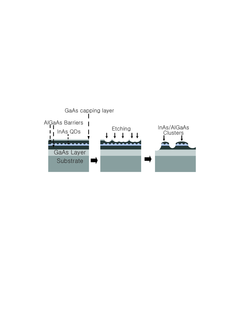
The InAs/AlGaAs QD-based nanoclusters were fabricated as follows. First, the InAs/AlGaAs QD structure was grown on a 100 nm thick GaAs buffer layer prepared on a GaAs (100) substrate as shown in Fig. 1. The InAs QDs were embedded in a 50 nm thick AlGaAs cladding layer. An additional 5 nm thick GaAs capping layer was also grown by molecular beam epitaxy. The density of the InAs QDs is typically about . Kim00 Then, by dry etching of the QD structure by using an inductively coupled plasma reactive ion etcher (RIE) Cho04 , InAs/AlGaAs QD structure was etched down to the boundary region between the InAs QDs and the lower AlGaAs barrier. Note that during the etching process, the etched surface is not usually smooth in the nano-scale, which results in the nanoclusters containing isolated InAs/AlGaAs QDs as shown in Fig. 1.
For optical pumping of QDs, a Ti:Sapphire laser was used, which was operated at the photon energy of 1.67 eV. This laser light was coupled to a single-mode optical fiber and guided to a chemically etched sharp fiber tip, where an 100-nm gold-coated aperture was fabricated. Ohtsu98 Such a nanometer-scale light source generated by the aperture-fabricated fiber probe makes it possible to excite nanoclusters in small area with nanometer-scale position selectivity. The resulting PL was collected by the same fiber so that any loss of spatial resolution due to diffusion could be minimized. Saiki99 ; Yu03 Both the sample and the fiber probe were enclosed in a cryostat and kept at 77 K. The PL was dispersed by a monochromator with 0.3 meV spectral resolution and detected by a liquid-nitrogen-cooled charge-coupled device camera to achieve high signal-to-noise ratio.
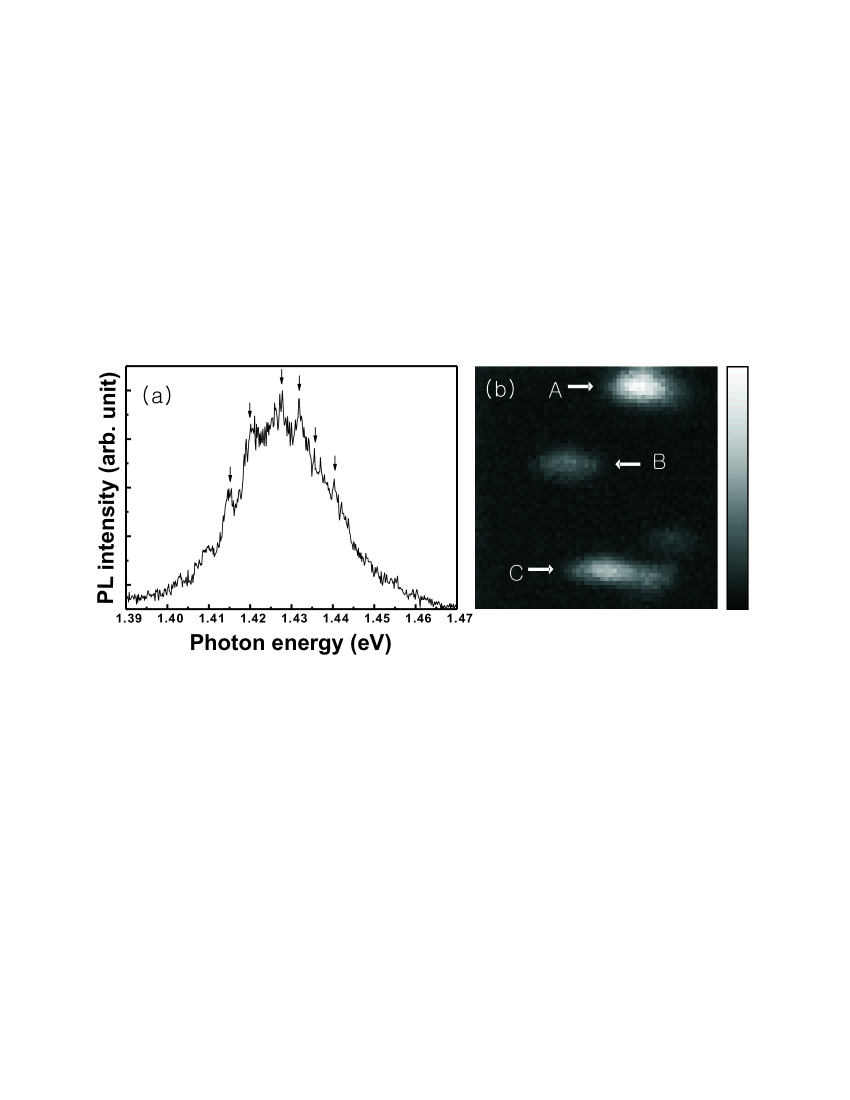
Figure 2(a) shows the PL spectrum of an InAs/AlGaAs QD-based nanocluster by employing NSOM. Although the PL peaks of single InAs QDs (marked by arrows in Fig. 2(a)) are superimposed on the broad background emission spectrum, they are not clearly resolved due to inhomogeneous broadening at relatively high temperature (77 K). Note that in order to perform high-resolution single QD spectroscopy at this temperature, both an apertured probe with a few hundred nm in diameter and a sample with a masking layer having a few hundred nm apertures are necessary, which reduce the number of excited single QDs as well as the transmission of the excitation laser, as reported in Ref. Yu03, . The spatial PL image of the nanoclusters was also obtained and presented in Fig. 2(b), where the selected PL energy is 1.4271 eV and the scan area is . The full width at half maximum (FWHM) along the horizontal axis of the bright objects marked by the arrows A, B, and C in Fig. 2(b) are 941, 1135 and 1471 nm, respectively. It indicates that the nanoclusters were formed nonuniformly during the etching process.
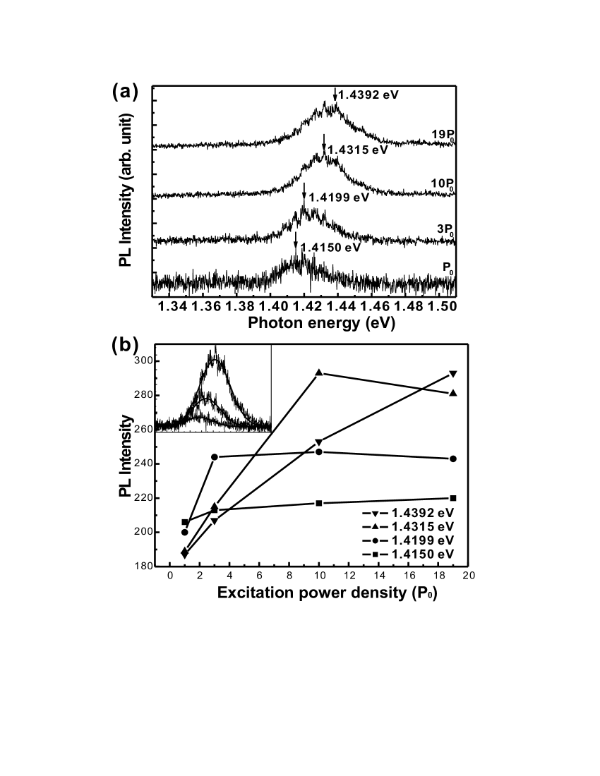
Figure 3(a) presents the normalized PL spectra of a QD nanocluster obtained by increasing the excitation power density from to , where is 8.6 kW/cm2. As can be observed, the blueshift ( meV) and the linewidth broadening ( meV) are obtained as the excitation power is increased. For example, the center energy of the PL spectrum is shifted from 1.4175 eV at to 1.4335 eV at . The inset of Fig. 3(b) shows the unnormalized PL spectra of QD nanocluster as the excitation is increased from to . Note that one can clearly observe the plateau region of the PL spectrum ( 1.4315 eV) becomes increasingly broadened and also the PL intensity is enhanced with the excitation power density. Figure 3(b) shows the intensity saturation for the lower PL energy states (1.4150 and 1.4199 eV) as well as the intensity increase for the higher states (1.4315 and 1.4392 eV) with the power density from to . Note that these phenomena are well known characteristics of the band-filling effect, as reported by other works. Castrillo95 ; Wang01 ; Sugisaki01 ; Masumoto02 ; Cingolani93 ; Xin99 Note also that a possible temperature increase of QD-nanocluster due to the heated probe at high excitation level may result in redshift of the PL spectra Jiang00 , which may eventually limit the blueshift of PL spectrum.
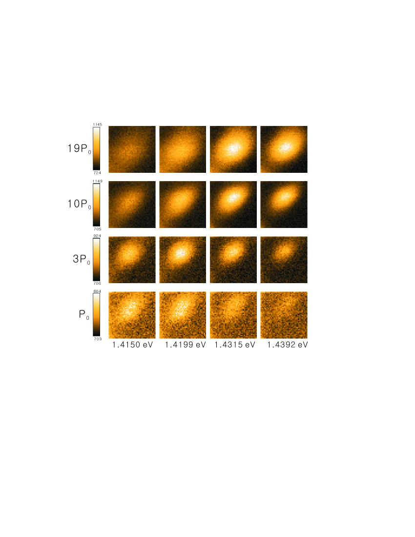
Figure 4 shows the two-dimensional spatial PL images, obtained for several energy states (marked by the arrows in Fig. 3(a)) of the nanocluster with respect to the excitation power density. The near-field PL images were obtained at 25 nm interval in scan area by using the 100-nm apertured fiber probe. Eah02 ; Yu03 Note that, in Fig. 4, the intensities of the PL images are displayed on the same scale for each excitation level from to . The average FWHM along the horizontal-axis of the PL images is about 600 nm. As can be observed, excitons become spatially confined gradually from lower energy state (1.4150 eV) to higher energy state (1.4392 eV) as the excitation power is increased from to , which may be attributed to the band-filling effect of semiconductor nanostructures. In order to have a quantitative understanding of the various PL images presented in Fig. 4, we present the analyzed excitation-level dependence of the intensity as well as the FWHM of the PL images in Fig. 5.
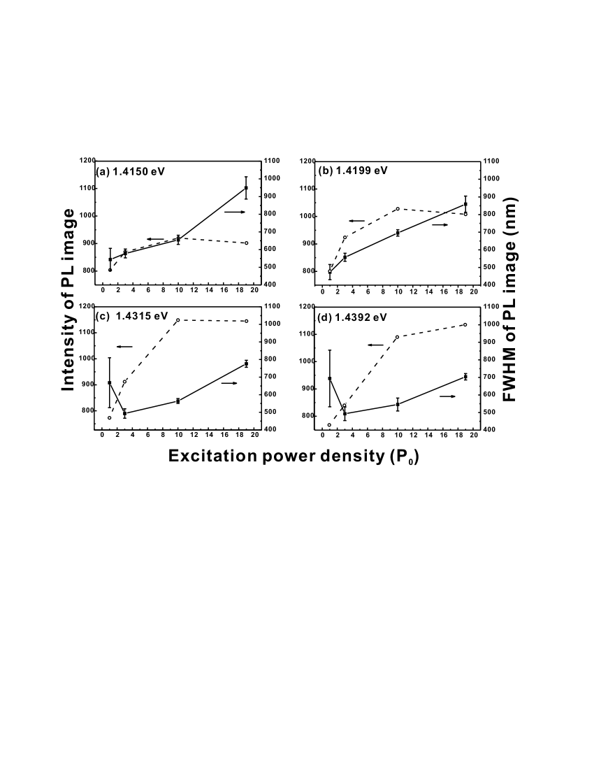
Figures 5(a) and (b) show that the intensity of the PL images is saturated as the excitation power density is increased, whereas the FWHM is gradually increased. This indicates that the PL images at 1.4150 and 1.4199 eV energy in Fig. 4 are dispersed and spread with the excitation power density. In case of Figs. 5(c) and (d), on the other hand, the intensity increases more rapidly than in Figs. 5(a) and (b). Especially, the PL intensity at 1.4392 eV in Fig. 5(d) increases almost monotonically, in contrast to the height decrease or saturation for other energy states in Figs. 5(a), (b), and (c), at a given excitation level of . Moreover, the FWHM and its measurement uncertainty in Figs. 5(c) and (d) decrease rather rapidly at the excitation power density from to , but the FWHM starts increasing above excitation. These results indicate that while the PL images at 1.4315 and 1.4392 eV energies in Fig. 4 appear at the excitation level from to , the confining ratio of the excitons in these energy states (1.4315 and 1.4392 eV) is enhanced beyond . In other words, Fig. 4 shows that the dominant PL energies from the InAs/AlGaAs QD-based nanocluster are gradually changed from the lower energy states to the higher energy ones with the excitation pumping level.
In conclusion, we have studied the band-filling effect in the InAs/AlGaAs QD-based nanoclusters, as observed by modification of the spatial distributions of the PL images. In particular, the PL energy states of the nanoculster are gradually changed from the lower energy states to the higher energy states at a proper excitation pumping level. The present work may be useful in application of tunable energy states to optical nano-devices.
Acknowledgements.
This work was supported by the Korean Ministry of Science and Technology through the Creative Research Initiatives Program.References
- (1) P. Castrillo, D. Hessman, M.-E. Piston, S. Anand, N. Carlsson, W. Seifert, and L. Samuleson, Appl. Phys. Lett. 67, 1905 (1995).
- (2) M. Sugisaki, H.-W. Ren, S. V. Nair, K. Nishi, Y. Masumoto, Solid State Commun. 117, 435 (2001).
- (3) Y. Masumoto and T. Takaghara, Semiconductor Quantum Dots: Physics, Spectroscopy and Application (Springer-Verlag, New York, 2002).
- (4) L. Mller-Kirsch, R. Heitz, A. Schliwa, O. Stiter, D. Bimberg, H. Kirmse, and W. Neumann, Appl. Phys. Lett. 78, 1418 (2001).
- (5) R. Cingolani, R. Rinaldi, M. Ferrara, G. C. La Rocca, H. Lage, D. Heitmann, K. Ploog, and H. Kalt, Phys. Rev. B 48, 14331 (1993).
- (6) H. P. Xin, K. L. Kavanagh, Z. Q. Zhu, and C. W. Tu, Appl. Phys. Lett. 74, 2337 (1999).
- (7) A. Chavez-Pirson, J. Temmyo, H. Kamada, H.Gotoh, and H. Ando, Appl. Phys. Lett. 72, 3494 (1998).
- (8) Y. Toda, M. Kourogi, M. Ohtsu, Y. Nagamue, and Y. Arakawa, Appl. Phys. Lett. 69, 827 (1996).
- (9) T. Saiki and K. Matsuda, Appl. Phys. Lett. 74, 2773 (1999).
- (10) Y.-J. Yu, W. Jhe, and Y. Arakawa, Appl. Phys. Lett. 83, 3024 (2003).
- (11) S.-K. Eah, W. Jhe, and Y. Arakawa, Appl. Phys. Lett. 80, 2779 (2002).
- (12) Y. S. Kim, U. H. Lee, D. Lee, S. J. Rhee, Y. A. Leem, H. S. Ko, D. H. Kim, and J. C. Woo, J. Appl. Phys. 87, 241 (2000).
- (13) C.-O. Cho and Y.-G. Roh and Y. Park and H. J. Jeon and B.-S. Lee and H.-W. Kim and Y.-H. Choe, Jpn. J. Appl. Phys. 43, 1384 (2004).
- (14) M. Ohtsu, Near-Field Nano/Atom Optics and Technology (Springer-Verlag, 1998).
- (15) W. H. Jiang, X. L. Ye, B. Xu, H. Z. Xu, D. Ding, J. B. Liang, and Z. G. Wang, J. Appl. Phys. 88, 2529 (2000).