2D Detectors for Particle Physics and for Imaging Applications
Abstract
The demands on detectors for particle detection as well as for medical and astronomical X-ray imaging are continuously pushing the development of novel pixel detectors. The state of the art in pixel detector technology to date are hybrid pixel detectors in which sensor and read-out integrated circuits are processed on different substrates and connected via high density interconnect structures. While these detectors are technologically mastered such that large scale particle detectors can be and are being built, the demands for improved performance for the next generation particle detectors ask for the development of monolithic or semi-monolithic approaches. Given the fact that the demands for medical imaging are different in some key aspects, developments for these applications, which started as particle physics spin-off, are becomming rather independent. New approaches are leading to novel signal processing concepts and interconnect technologies to satisfy the need for very high dynamic range and large area detectors. The present state in hybrid and (semi-)monolithic pixel detector development and their different approaches for particle physics and imaging application is reviewed.
keywords:
pixel detectors , semiconductor detectors , hybrid pixels , monolithic pixels , tracking , imaging , x-ray detectorPACS:
07.77.Ka , 07.85.Fv , 29.40.Gx , 87.57.-s , 87.59.-e , 87.66.Pm1 Hybrid Pixel Detectors for tracking applications
The development of hybrid pixel detectors over the last 10 years was mainly pushed by the specifications for the vertex detectors for the large high energy physics experiments ALICE [ALICE_pix, ALICE_Riedler], ATLAS [ATLAS_pix, ATLAS_Gemme], CMS [CMS_pix, CMS_Erdmann], LHCb [LHCb_pix] and fixed target experiment NA60 [NA60, NA60_Radermacher] at the Large Hadron Collider (LHC) at CERN and the BTeV detector at the TEVATRON [BTEV_pix]. All these experiments have a high demand on spatial resolution, timing precision and radiation tolerance. Also the feasibility of building large detector areas (up to 2m2) had to be proven. The hybrid pixel technology, where electronic chip and sensor elements are on different substrates which are connected via flip-chip assembly, showed to be mature enough to comply with all these demands. The pixel detectors, which are closest to the interaction region of a collider experiment, comprise of typically 2 to 3 cylindrical layers and additional disk layers for the forward and backward region. The pixel sizes are between 50m 400m and 100m 150m for the mentioned experiments to achieve the spatial resolution which is required for efficient identification of short lived particles (b-tagging for Higgs and SUSY signals) and robust event reconstruction at high luminosities.
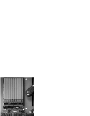
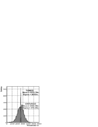
Apart from the electronical requirements on the pixel electronics [blanquart03] like low power consumption ( 50W per pixel), low noise and threshold dispersion (together 200e), zero suppression in every pixel, on-chip hit buffering and sufficient timing precision for LHC bunch crossing rates (25 ns), the essential radiation hardness has been a major challenge for the design of front-end chips. This could be achieved with special design techniques and the use of deep submicron CMOS technologies, which superseeded dedicated radhard processes. Figure 1 shows a picture of a prototype ATLAS pixel chip and a measurement of the threshold distribution which is a measure for the homogeneity of the chip response. The dispersion of about 600 e- can be lowered to below 50 e- by a 7-bit tuning feature implemented in the chip. This is well below the electronic noise of about 170 e-. However the minimum operational threshold is limited to 1500 e due to the crosstalk between the digital and the analog part of the pixel chip.
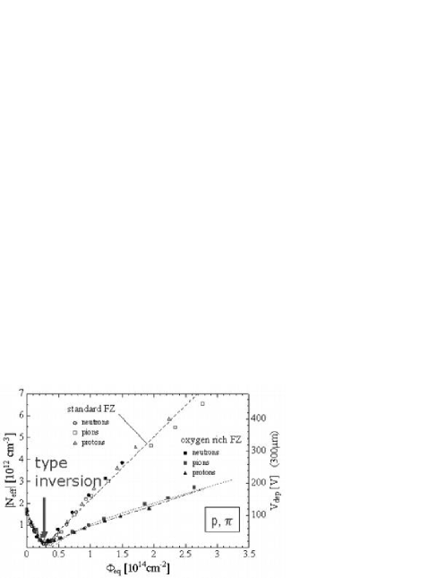
Figure 2 shows the improvement of the radiation tolerance of the sensor material by the use of oxygenated silicon which has less sensitivity to non-ionizing energy loss of charged particles [oxysilicon]. The fact that radiation damage caused by neutrons is the same as with standard silicon is not fully understood yet. The sensor pixels are implanted as electrodes in n-bulk material. After type inversion which occurs after about cm-2 the diode junction is at the electrode side, allowing the partial depleted operation of the detector with less than 600 V after ten years of LHC operation.
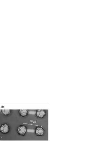
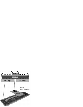
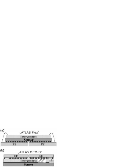
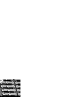
The assembly of the sensor modules is done by fine pitch flip-chip bonding the electronic chips and the sensor. Mainly two different technologies are used to build sensor modules in large scales: Solder (PbSn) bump bonding [PbSn_bumping] with reflow and Indium bump bonding [Indium_bumping] with optional reflow [In-reflow_bumping] and thermal compression. Fig. 3 shows rows of m pitch bumps obtained by these techniques. All technologies have been successfully used with 8” IC-wafers and 4” sensor wafers. A module for the ATLAS or CMS pixel detector is composed of 16 front-end chips bump-bonded to one silicon sensor with an area of typically 2 cm 6.5 cm. As shown in Fig. 4 a kapton flex circuit which supports a module control chip is glued on the backside of the sensor. Wire bonds connect the front-end chip I/O lines and a high density interconnect adapter (pigtail) to the flex circuit.
To minimize the radiation induced damage of the sensors due to the harsh radiation environment the mechanical support structure for the modules also has to provide cooling to temperatures below the freezing point. To compensate this additional material budget the front-end chips are thinned down to 180 m giving a total thickness of the module at normal incidence of about ( is the radiation length which specifies the average lenght of path in a specific material in which a relativistic charged particle will loose 67 of its energy).
2 Imaging with Hybrid Pixel Detectors
With the design of pixel chip electronics for vertex trackers the capability of detecting individual radiation quanta made hybrid pixel detectors also very attractive for non-HEP applications like medical X-ray imagers or synchrotron radiation detectors. The counting principle leads to superior performance of such detectors compared to standard film-foil or scintillator-CCD systems that are normally used for imaging: an in principal unlimited dynamic range and full linearity in their response function.
While in tracking applications the timing information (and optional the energy loss) of an incident particle is measured within every pixel, most of the present imaging applications are based on counting the individual quanta for a certain exposure time intervall. Therefore the first implementations of counting pixel detectors simply replaced the digital part of the pixel electronic of a vertex tracker pixel chip, which generates the timestamp for each individual event, by a counter [MEDIPIX1][MPEC_ref]. The same principle is also used for protein-crystallography with synchrotron radiation [Graafsma_Portland, 3Dwestbrook]. But for successful development of an optimized imaging system based on a hybrid pixel detector one has to obey the different demands for both application areas. Table 1 gives a summary of the different system aspects and subsequent demands on the pixel electronics and sensor charcteristics for tracking and imaging applications, respectively.
![[Uncaptioned image]](/html/physics/0503088/assets/x9.png)
Conventional X-ray imagers integrate the energy of the absorbed quanta. The so called Active Matrix Flat Panel Imager [flatpanel1, flatpanel2, a-Se, flatpanel4], which represents the state-of-the-art in digital X-ray detectors, exploits two different detection methods: indirect conversion, where a scintillator (e.g. CsI) is deposited atop a TFT photo diode array, and direct conversion where an absorber (e.g. Selenium) converts the incident X-rays to a charge which is collected with an TFT capacitor array [flatpanel3]. Due to the principle of accumulating the incident particles, the rate capability of integrating imagers is practically unlimited. To be competitive with these detectors the counting approach needs to meet the high count rates ( 10 MHz/mm2) and the high dynamic range of at least 15 bit. In addition these detectors should combine low noise and low thresholds with a very low threshold dispersion to allow homogenous imaging.
Medical Imaging
Besides the superior signal to noise figures, which reach the quantum limit, the counting principle offers the fundamental advantage of attaining and exploiting an additional spectral information from the incident X-ray photons. In the simplest implementation a differential energy measurement is realized with a double threshold [MPEC-windowing1, MPEC-windowing2, MEDIPIX2] which can enhance the contrast of an image as the X-ray energy spectrum is different behind different absorbers (e.g. bone or soft tissue). The next step towards the use of the spectral information could be the implementation of more discrete energy bins and the use of an energy weighting technique which has the potential to enhance the image contrast [MEDIPIX_EWT]. A homogeneous response of the absorber material, low threshold dispersion and control of the charge shared between adjacent pixels is crucial however. Another issue – especially with the dense electronics of a hybrid pixel detector – is the digital noise (crosstalk between the digital and the analog part), which is still the limitinig factor for a low threshold operation of a hybrid pixel detector system.
Also a high photon absorption efficiency is mandatory for radiography requiring the use of high-Z sensor materials like CdTe or CZT. With these materials the development of large area detectors and their hybridization is still a challenging task.
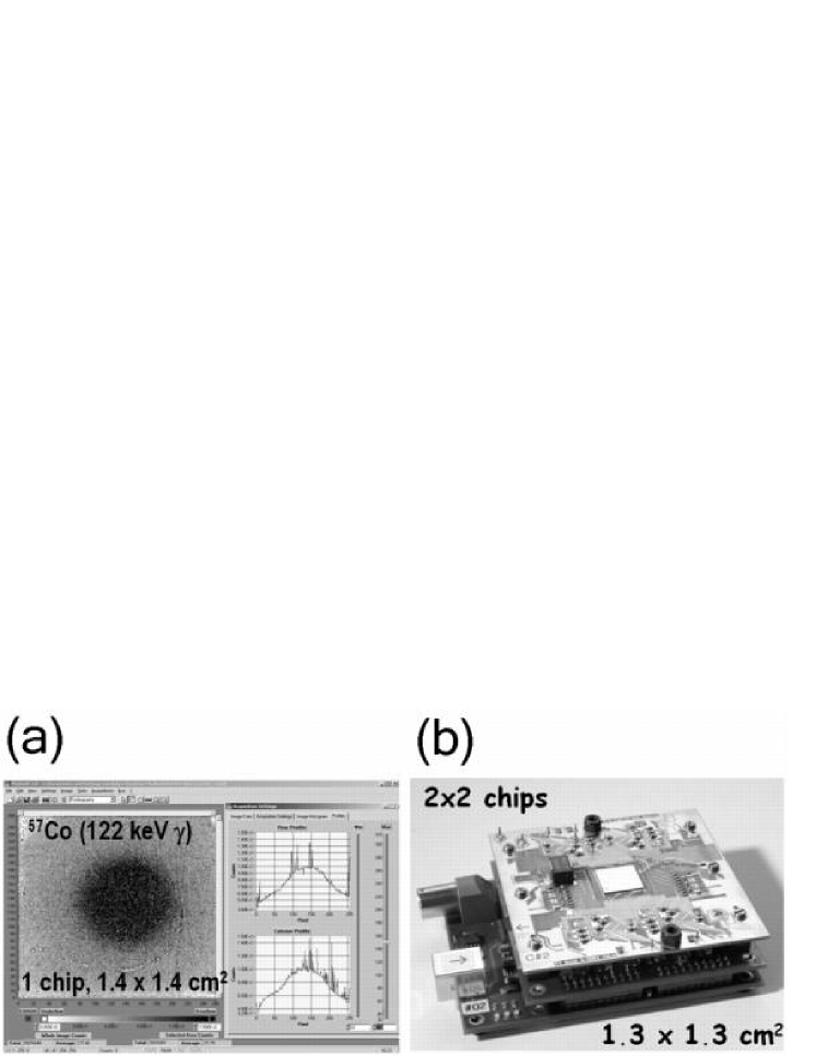
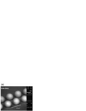
There are serveral counting pixel system development efforts for medical applications. Among those projects two chip developments exhibit a rather mature R&D status: the MEDIPIX collaboration [MEDIPIX, MEDIPIX2] uses the MEDIPIX2 chip with 256256, 5555m2 pixels fabricated in m technology, energy windowing via two tunable discriminator thresholds, and a 13 bit counter. The maximum count rate per pixel is about 1 MHz. Fig. 5(a) shows an image of a 57Co (122 keV ) 1 mm diameter point source obtained with the Medipix2 single chip bonded to a 14x14 mm2 CdTe sensor [MEDIPIX_Portland]. A Multi-Chip module with 2x2 chips using high-Z CdTe sensors with the MPEC chip [MPEC_Portland] is shown in Fig. 5(b). The MPEC chip features pixels (200200m2), double threshold operation, 18-bit counting at 1 MHz per pixel as well as low noise values (120e with CdTe sensor) and threshold dispersion (e after tuning) [MPEC_ref, MPEC_Portland]. A technical issue here is the bumping of individual die CdTe sensors which has been solved using Au-stud bumping with In-topping [MPEC_CdTe].
Protein Crystallography
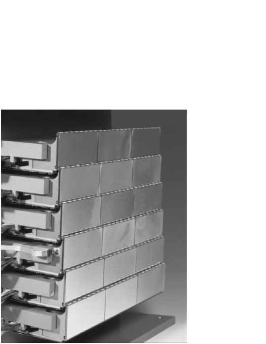
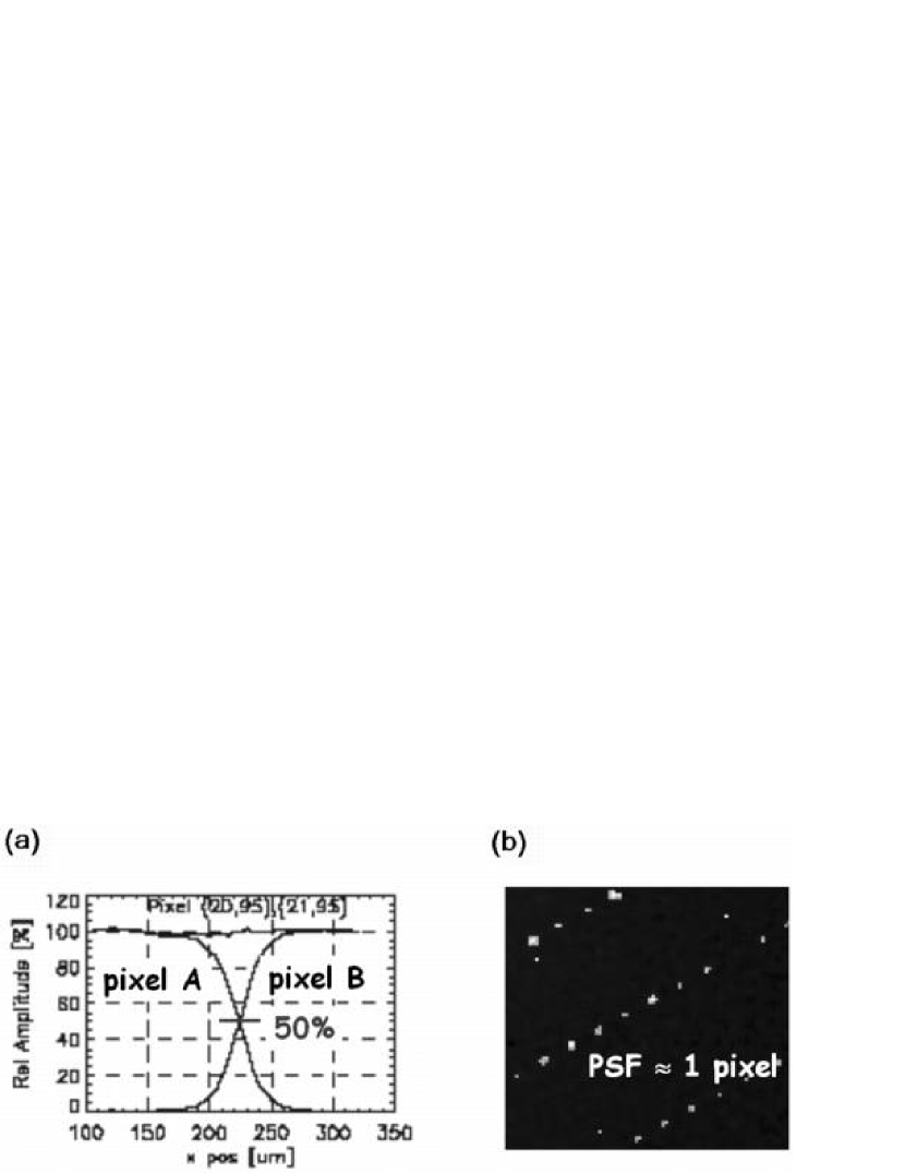
Protein Chrystallography is another appealing application for counting pixel detectors. For the imaging of Bragg spots from X-ray photons of 12 keV (corresponding to resolutions at the 1 range) or higher, scattered off protein crystals, with high rate (1-1.5 MHz/pixel) and high dynamic range [Graafsma_Portland], photon counting detectors have fundamental advantages over conventional integrating detector systems. That is the high linearity of the counting method and the absence of so-called ”blooming-effects”, i.e. the response of non-hit pixels in the close neighborhood of a Bragg spot. For a typical Bragg spot the size of a diffraction maximum is m, calling for pixel sizes in the order of m, which is well achievable with today’s hybrid pixel detectors. A systematic limitation and difficulty is the problem that homogeneous hit/count responses in all pixels, also for hits at the pixel boundaries or between pixels where charge sharing plays a role must be maintained by delicate threshold tuning (Fig. 7(a)). Counting pixel developments are made for ESRF (Grenoble, France) [XPAD1, XPAD2] and SLS (Swiss Light Source at the Paul-Scherrer Institute, Switzerland) beam lines. A photograph of the PILATUS 1M detector [PILATUS] at the SLS ( 106 m m pixels, 18 modules, 2024 cm2 area) is shown in Fig. 6. It is the first large scale hybrid pixel detector in operation. Fig. 7(b) shows some Bragg spots obtained from a Lysozyme crystal with 10s exposure to 12 keV sychrotron X-rays [PILATUS_Portland].
3 Trends in Hybrid Pixel Detectors
With their mature technology Hybrid Pixel detectors prove to be the State of the Art in 2D sensor systems. However there are some general limitations and challenges for special applications. Hybrid Pixel detectors are an expensive and complex technology, last but not least due to yield issues of the many production steps (chip, sensor, bumping, flip-chip). Also the achievable spatial resolution is limited to about m with pixel geometries of m (with analog R/O). Where large area detectors are built, complex mechanical structures are required to provide seamless coverage of the solid angle. For imaging applications it is even more crucuial to use seamless large area detectors without tiling to optimize the image reconstruction. In addition, tracking applications impose a tight specification on the material budget which is not optimal with Hybrid Pixel detectors. Also the inevitable cooling for operation of Si detectors under strong irradiation adds to that material budget. Several ideas and developments are being pursued to address some of the issues stated above:
HAPS
Hybrid (Active) Pixel Sensors (HAPS) [HAPS] exploit capacitive coupling between pixels – similar to the same technique often used with silicon micro strip detectors – to obtain smaller pixel cells and pixel pitch with a larger readout pitch resulting in interleaved pixels. The pixel pitch is designed for best spatial resolution using charge sharing between neighbors while the readout pitch is tailored to the needs for the size of the front-end electronics cell. Sensor studies lead to resolutions between 3m and 10m which could be obtained with pixel (readout) pitches of 100m (200m).
MCM-D
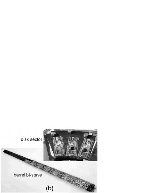
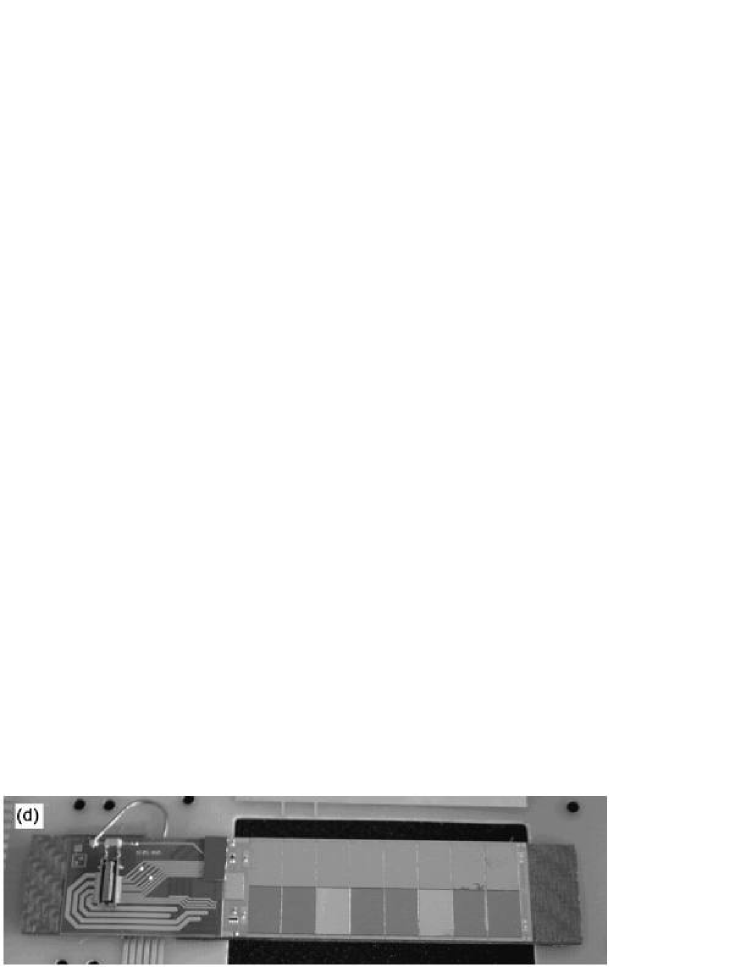
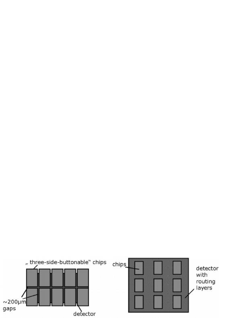
The present hybrid-pixel modules of the LHC experiments use an additional flex-kapton fine-print layer on top of the Si-sensor (Fig. 8(a)) to provide power and signal distribution to and from the module front-end chips. An alternative to the flex-kapton solution is the so-called Multi-Chip-Module Technology deposited on Si-substrate (MCM-D) [MCMD1]. A multi-conductor-layer structure is built up on the silicon sensor. This allows to bury all bus structures in four layers in the inactive area of the module thus avoiding the kapton flex layer and any wire bonding at the expense of a small thickness increase of (Fig. 8(b)). The extra freedom in routing also allows to design pixel detectors which have the same pixel dimensions throughout the sensor. Fig. 8(c) shows a scanning electron microphotograph (courtesy IZM, Berlin) of an MCM-D via structure, and Fig. 8(d) shows the photograph of an assembled ATLAS MCM-D module [MCMD3]. This concept also provides the possibility to build detector modules which have non equal area ratios of sensor and electronic chips when the routing layer implements a fan-out between the electronic pixels and the corresponding sensor elements. With this approach it would be possible to build large area modules with nm chips and almost 100% active area (Fig. 9).
3-D Silicon Detectors, Active Edge
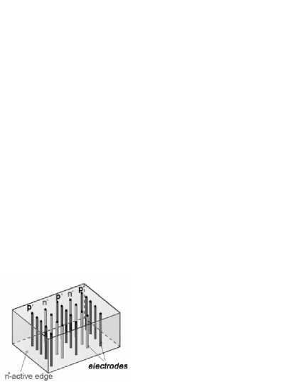
So called 3-D detectors provide a lateral drift field between their needle like alternating p+ and n+ electrodes which have a typical pitch of 50m [3D-parker] (Fig. 10). Thus they exhibit a very fast charge collection (1 - 2 ns) at low depletion voltages ( 10 V) which make them well suited for harsh radiation environments. They are build using micromechanical systems technology involving the use of support wafers and reactive ion etching which makes their fabrication more complex compared to standard planar processes. The same technology can be used to extend the sensitive area of a detector within 10 m of its edge which leads to a so called active-edge detector [active_edge].
4 Monolithic and Semi-Monolithic Pixel Detectors
The ultimate goal of a detector development would be the integration of sensor, amplifying electronics and read-out logic on one single substrate in a technology which would be commercially available. So far different attempts to develop such monolithic pixel detectors have been undertaken. Much of these efforts are influenced by RD for vertex tracking detectors at future colliders such as a International Linear Collider (ILC) [TESLA-TDR]. These detectors require a very low material budget per layer (1 X0), small pixel sizes (20mm) and a very high rate capability (80 hits/mm2/ms) yielding challenging requirements on the sensor and the electronics circuitry.
The different monolithic approaches can be characterized according to some fundamental features regarding the charge collection process and the complexity of electronic circuitry. One distinction is based upon the fact whether full CMOS circuitry is allowed (also in the pixel active area) and if the approach is based on or at least compatible with a standard process technology. The other basic criterion is the charge collection process and thus the amount (and uniformity) of the generated signal. Charge collection occurs either in a fully depleted bulk providing a large signal or in a thin undepleted epi-layer, respectively amorphous-Si layer, which leads to smaller signals. The above mentioned ultimate monolithic goal would be fulfilled with a full CMOS commercial standard device with charge collection in a fully depleted bulk.
-
-
Non-standard CMOS on high resistivity bulk
The first monolithic pixel detector was successfully operated in a particle beam already in 1992 [parker92] using a high resistivity p-type bulk p-i-n detector in which the junction had been created by an n-type diffusion layer. On one side, an array of ohmic contacts to the substrate served as collection electrodes. Due to this only pMOS transistor circuits sitting in n-wells were possible to be integrated in the active area. The technology was certainly non-standard and non-commercial. No further development emerged. -
-
Standard CMOS technology with charge collection in epi-layer
Certain CMOS technologies offer a lightly doped epitaxial silicon layer of a few to 15m thickness between the low resistivity silicon bulk and the planar processing layer which can be used for charge collection [meynants98, MAPS1, MAPS2]. The generated charge is kept in a thin epi-layer atop the low resistivity silicon bulk by potential wells at the boundary and reaches an n-well collection diode by thermal diffusion (cf. Fig. 11(a)). The sensor is depleted only directly under the n-well diode. The signal charge is hence very small (1000e) and mostly incomplete; low noise electronics is the challenge in this development. Due to the diffusion process the charge collecting time might also be an issue for high rate applications. Collaborating groups around IReSLEPSI [LEPSI1, LEPSI-Portland], RAL [RAL-Vertex03] and Irvine-LBNL-Ohio [kleinfelder03] use similar approaches to develop large scale CMOS active pixels also called MAPS (Monolithic Active Pixel Sensors) [MAPS1]. Prototype detectors have been produced in m, m and m CMOS technologies [Dulinski03, AGay03].Matrix readout of MAPS is performed using a standard 3-transistor circuit (line select, source-follower stage, reset) commonly employed by CMOS matrix devices, but can also include current amplification and current memory [Dulinski03]. For an image two complete frames are subtracted from each other (correlated double sampling, CDS) which suppresses switching and low frequency noise. Noise figures of 10-30e and S/N 20 have been achieved with spatial resolutions below 5m. Regarding radiation hardness MAPS appear to sustain non-ionizing radiation (NIEL) to 1012neq while the effects of ionizing radiation damage (IEL) are at present still under investigation. The present focus of further development lies in making larger area devices for instance by stitching over reticle boundaries [AGay03], increasing the charge collection performance in the epi-layer by triple-well [RAL-Vertex03], photo-gate [Kleinfelder-Portland], and photo-FET [Dulinski03, LEPSI-Portland] techniques and developing a higher radiation tolerance. In addition, for applications like e.g. precise beam position monitoring in hadron therapy, devices with very thin entrance windows are needed to detect 20 keV electrons scattering off a thin metal foil held in the hadron beam. Such a thinned MAPS detector, which is also capable of autoradiographic tritium detection, is shown in Fig. 11(b).
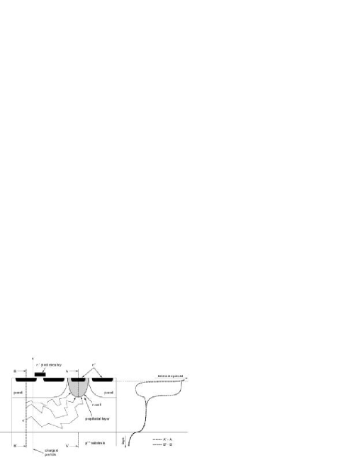
Figure 11: (a) Principle of an Monolithic Active Pixel Sensor (MAPS) targeting CMOS electronics with low resistivity bulk material. The charge is generated and collected by diffusion in the few m thin epitaxial Si-layer. (b) MAPS detector with 100 nm thin backside entrance window. Being a standard CMOS process this approach has the potential to build large area detectors at low costs (25 per cm2). On the other hand the thickness of the epi-layer is technology dependent and scales with the decreasing feature size of future processes hence further reducing the available signal charge. Another drawback of this approach is the fact that despite using CMOS technology the potential of full CMOS circuitry in the active area is not available (only nMOS) because of the n-well/p-epi collecting diode which does not permit other n-wells. Nevertheless improved readout concepts and device development for high rate particle detection at a linear collider are under development [TESLA-TDR]. As a concrete project for an experiment the STAR micro vertex detector upgrade plans the use of CMOS active pixels [Dulinski03].
-
-
Non-standard SOI on high resitivity bulk
To join the features of full charge collection and the utilization of true full CMOS circuitry the authors of [SOI-Portland] propose the development of sensors using a silicon-on-insulator (SOI) wafer with an high resestivity bulk material. SOI process technology which has been developed in favor for advanced high-speed and low-power circuits uses special wafers with a thin monolithic Si layer (50 nm – 1.5 m) atop a buried oxide (SiO2) layer. This layer effectively isolates the electronically active SOI layer from the bulk material rendering it a pure mechanical support. The idea of this development approach is to use a high resistivity material for the support wafer to achieve a fully depletable charge generation layer of suitable thickness (200–300m). The charge collection will be obtained by vias which connect the high resitivity bulk with electronic circuits through the insulation layer (Fig. 12). Present results are based also on a non-standard SOI technology but this interesting development is still in its beginnings and might have the potential to become compatible with commercial process technologies [SOI_Hiroshima].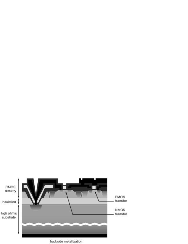
Figure 12: Cross section through a monolithic CMOS on SOI pixel detector using high resistivity silicon bulk insulated from the low resistivity CMOS layer with connecting vias in between [HAPS-SOI, SOI-Portland]. -
-
Amorphous silicon on standard CMOS ASICs
A development approach which is compatible with standard CMOS technology is based on the deposition of the sensor material as an amorphous film direct on the surface of the readout ASIC. Hydrogenated amorphous-Silicon (a-Si:H) has been studied as a sensor material long ago and has gained interest again [theil2001, jarron02] with the advancement in low noise, low power electronics. With the deposited film being only 30m thick the collected charge is in the range of only 500-1500 electrons which makes ultra low-noise electronic inevitable. A cross section through a typical a-Si:H device is shown in Fig. 13. Although not a entirely monolithic concept the amorphous silicon on standard CMOS ASICs approach lacks the demanding process of hybridization. Also the radiation hardness of these detectors appears to be very high 1015cm-2 due to the defect tolerance and defect reversing ability of the amorphous structure and the larger band gap (1.8 eV). For high-Z applications poly-crystalline HgI2 constitutes a possible semiconductor film material. The potential advantages are small thickness, radiation hardness, and low cost. The development is still in its beginnings and the main challenge – beneath low noise VLSI design – is the quality of the amorphous material and the technology of its deposition.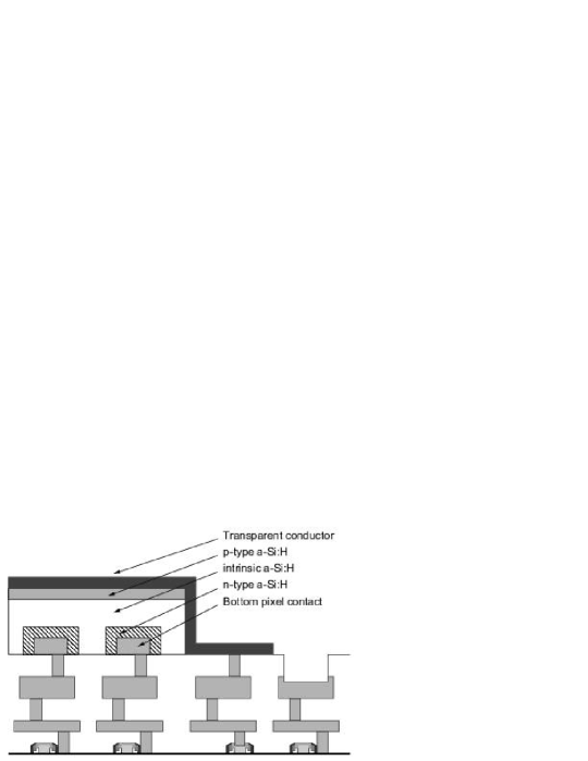
Figure 13: Cross section through a structure using amorphous silicon on top of standard CMOS VLSI electronics [theil2001, jarron02]. -
-
Amplification transistor implanted in high resistivity bulk
The basic idea of this development approach is the integration of the first amplifying transistor of the readout electronic into the sensor substrate. This so-called DEPFET pixel sensors [kemmer87] have a JFET or MOSFET transistor implanted in every pixel on a sidewards depleted [gatti84] bulk. Electrons generated by radiation in the bulk are collected in a potential minimum underneath the transistor. This potential minimum acts as an internal gate and the collected charge is modulating the channel current (Fig. 14). With additional contacts of the external gate and a so-called clear contact individual transistors in a 2-D matrix can be selected for readout and subsequently reseted. The bulk is fully depleted rendering large signals and at the same time the small capacitance of the internal gate offers low noise operation. With round single pixel structures noise figures of 2.2e at room temperature and energy resolutions of 131 eV for 6 keV X-rays have been obtained [depfet_IEEE03]. This features make DEPFET pixel detectors a competitive sensor system for applications which demand excellent energy resolution like X-ray astronomy [holl02] or biomedical autoradiography [ulrici03]. Also for the use as a vertex detector at the Future Linear Collider the DEPFET pixel detectors are under investigation [DEPFET-TESLA, depfet_IEEE03]. They would allow for thinned detectors (50m [laci04]) to comply with the tight material budget and a very low power operation of a row-wise switched matrix [Trimpl02, depfet_IEEE03]. The sensor technology is non-standard and the operation of DEPFET pixel detectors requires separate steering and amplification ICs.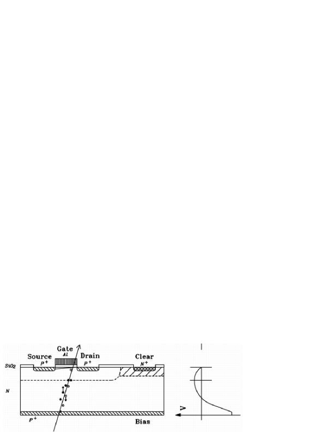
Figure 14: Principle of operation of a DEPFET pixel structure based on a sidewards depleted detector substrate material with an embedded planar field effect transistor. Cross section (left) of half a pixel with symmetry axis at the left side, and potential profile (right). 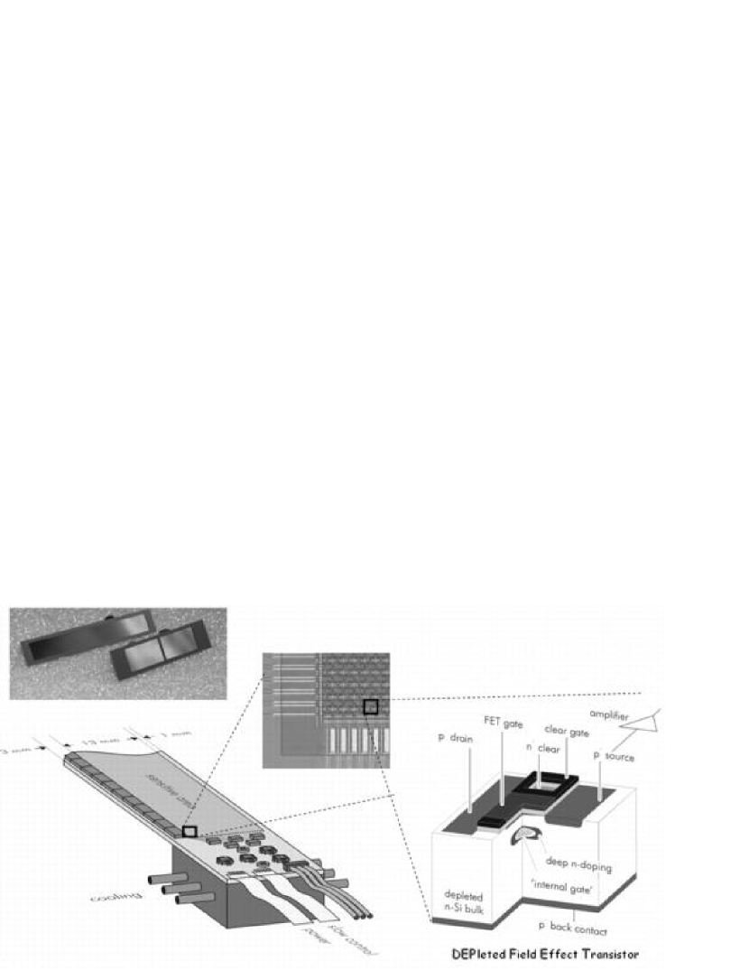
Figure 15: Sketch of a TESLA first layer module with thinned sensitive area supported by a silicon frame. The enlarged view show a DEPFET matrix and a DEPFET double pixel structure (20x30m2 pixel size), respectively. The photo (upper left) shows silicon diode structures thinned to 50m thickness by anisotropic etching [laci04] in a 300m thick frame.
5 Summary
The development of Hybrid Pixel technology had its origin in the demand for high performance vertex detectors for particle physics experiments. Along with it came large advancements in the development of low noise electronics, hybridization technology and understanding and control of radiation effects in sensor material and readout electronics. Also new application areas like X-ray astronomy, medical imaging and protein chrystallography emerged which require well adapted electronic concepts to cope with the varying demands on energy resolution and rate capability. This new range of applications and the increasing demand on the performance of future vertex detectors leads to new development trends. Some of them are enhancements to the Hybrid Pixel technology, as the sensor and electronic chip are still different entities: MCM-D structures allow large area modules and 3-D sensors with active edges improve the active/inactive area ratio and the radiation tolerance. Other interesting developments lead to monolithic detetion systems: MAPS sensors which employ the epi-layer of a standard CMOS technology for signal detection, the deposition of thin films like amorphous-Si on CMOS ASICs and the use of a CMOS-SOI process on a wafer with high resistivity bulk material. A semi-monolithic approach are the DEPFET pixels which integrate active transistors on a high resistivity bulk which are steered via external ASICs.