Macroscopic coherence effects in a mesoscopic system: Weak localization of thin silver films in an undergraduate lab
Abstract
We present an undergraduate lab that investigates weak localization in thin silver films. The films prepared in our lab have thickness, , between Å, a mesoscopic length scale. At low temperatures, the inelastic dephasing length for electrons, , exceeds the thickness of the film (), and the films are then quasi-2D in nature. In this situation, theory predicts specific corrections to the Drude conductivity due to coherent interference between conducting electrons’ wavefunctions, a macroscopically observable effect known as weak localization. This correction can be destroyed with the application of a magnetic field, and the resulting magnetoresistance curve provides information about electron transport in the film. This lab is suitable for Junior or Senior level students in an advanced undergraduate lab course.
I Introduction
One of the many challenges in a senior level lab course is to simulate the research environment. The labs generally should be geared toward helping students transition from performing pre-packaged experiments to more independent experiments. However, experiments of this sort should be designed so that motivated students can succeed and can do so in a term or semester. With this in mind, we have designed a simple experiment for students to observe the phenomena of weak localization.
Weak localization is a macroscopically observable consequence of the quantum mechanical behavior of electrons. Electrons begin to localize around impurities at low temperatures because of an effect that can be described as a self-interference effect. As electrons scatter around during transport measurements, they hit impurities, and special paths for partially scattered electron waves add together to start localization of electrons. This effect of pre-localization is lumped under the term weak localization, and one consequence is that the bulk behavior of electrons is altered.
The bulk property that most clearly gives evidence for weak localization is the magnetoconductance signal, which is best seen in thin film samples at low temperatures (accessible with liquid helium). The magnetoconductance is a small correction to the bulk conductance of a sample, theoretically on the order of of the bulk conductance. In this lab, we discuss how samples are made and how the magnetoconductance is measured.
One of the goals of this lab is to teach students techniques for measuring small signals. Measuring small signals is a common occurrence in condensed matter experiments, and for experimental physicists in general, it is good to learn tricks for working with faint signals. In our experiment, the magnetoresistive signal we want to measure is swamped by the bulk resistance of the sample. To magnify this weak signal, we use a resistance bridge. The philosophy is simple: null out the large resistance signal due to the bulk conductance and amplify the remaining signal due to the magnetoresistance. In addition to discussing the bridge, we also review sources of noise that can arise in the bridge, such as ground loops, and how to design the bridge to eliminate them.
Typical students’ results and a brief interpretation of these results are then discussed. We find that for the Ag thin film samples made in our lab, students observe weak localization with spin effects at temperatures below about 14 K. Above 14 K, phonons destroy the spin effects, and spinless weak localization is observed.
II Theory
Weak localization is a correction to the Drude conductivity. Before we discuss the correction, let us review the basic Drude prediction and the physical assumptions that lead to it.
II.1 Drude conductivity
If we apply an electric field inside a normal metal, that field will drive an electrical current. The current density is related to the field by
where is called the conductivity. Materials with high conductivity allow large currents for a given field, whereas materials with lower conductivities allow lower current densities.
A formula for the conductivity was derived by Drude ref:Drude , based on some very simple assumptions about the microscopic properties of metals. If the current is carried by electrons, then the current density is just
where is the number of electrons per unit volume, is the electric charge on a single electron, and is the average velocity of the electrons. Now, we need to calculate this average velocity. To do so, let’s assume that the electrons move inside the metal ballistically until they run into something. The electric field provides a force on the electrons given by , and the equation of motion is then
If we know an electron’s velocity at time , we can calculate it at a later time , provided it does not run into anything.
For this particular electron, let’s assume that just before it ran into something inside the metal (an impurity or phonon, for example) and bounced off. Moreover, let’s assume that, just after the collision, the velocity of the electron is completely random. This means that, on average,
With the assumption of isotropic scattering, the average velocity of all the electrons inside a metal is easy to calculate.
where is the average time since the last scattering event. This ensemble average is independent of the time when we take the snapshot, and it gives the conductivity.
This expression is known as the Drude conductivity, after the scientist who first derived it. It relies on the assumption that, after a scattering event, an electron’s velocity is completely randomized. Put another way, the electron has no memory of its previous state after it suffers a collision inside the material. As we shall see, this assumption is good at room temperatures, but it breaks down when the temperature of the metal becomes very low. The cause of this breakdown is the wave nature of the electron, which did not play a role in the derivation of the Drude conductivity, and the resulting change in the conductivity is one of the few macroscopically observable consequences of the wave-particle duality of matter.
II.2 Coherent backscattering
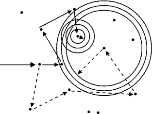
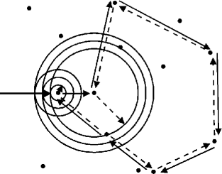
When we calculated the Drude conductivity, we assumed the electrons were point particles, obeying the laws of classical physics. In reality, however, electrons have associated with them wave functions, the square of the amplitude of which gives the probability of observing an electron. When the wave that describes an electron scatters off of some obstacle in its path, it produces partial waves emanating from that obstacle, much like ripples in a pond produced by a wave when it hits a stationary reed sticking out of the surface. These partial waves go on to strike other obstacles, impurities or defects in the case of a metal, and produce more partial waves. All of these partial waves add up, as waves do, to produce a complicated diffraction or interference pattern. For the most part, the phase between any two partial waves is random, and the partial waves, on average, add incoherently (see Figure 1). However, there is one direction in which the partial waves will always add up in phase, and that is the direction opposite that of the initial wave. This is because, for every path that takes a partial wave back to its origin, there is a complementary path with the same length that takes the same route, but in the opposite direction. The two partial waves that take these complementary paths will always add coherently (see Figure 2). The sum of all these complementary waves then gives a slightly stronger wave going backward relative to the initial direction. This corresponds to an enhanced probability of backscattering, which in turn reduces the conductivity below the Drude prediction.
If the metal is infinitely large and the electrons can maintain phase coherence over infinitely long complimentary paths, then the backscattering effect dominates the dynamics of the electrons, and the conductivity is completely suppressed. In this case, the metal becomes an insulator, and the electrons are trapped, or localized, by the disordered scattering centers. For samples with finite size, or more commonly finite coherence lengths, the backscattering gives rise to a small correction to the Drude conductivity. This small correction ought to be called “pre-localization,” but instead it is commonly referred to as “weak localization.”
The coherent backscattering effect can only occur if the phase of each partial wave is preserved as it goes around its path. At high temperatures, where most scattering events are off of phonons, coherent backscattering cannot occur. A magnetic field can also introduce a phase difference between the complementary paths, destroying the coherent backscattering and any correction to the Drude conductivity it produces. The resulting dependence of the conductivity on temperature or applied magnetic field is quite small even at liquid-helium temperatures, but it can be observed experimentally by employing a few basic low-noise techniques. In the experiment we will describe below, we use this weak-localization effect to teach some basic low-noise and small-signal-detection methods that are commonly used in many research labs.
II.3 Weak localization
A complete, quantitative derivation of the weak localization effect requires the use of quantum many-body theory and the quantum-field-theory techniques that go with it. This is beyond the scope of this paper, and we will just give the result here without derivation. See Ref. 2 or Ref.3 for a detailed treatment of the theory of weak localization.
The change in the conductance of a sample when a magnetic field is applied is called the magnetoconductance. This magnetoconductance is easiest to observe in a two-dimensional sample, where we can apply a magnetic field that is perpendicular to the sample and thus perpendicular to all of the complimentary, closed-loop paths that give rise to the coherent backscattering. For a thin film (a nearly two-dimensional sample), the magnetoconductance is
| (1) | |||||
where is the thickness of the film, , and is the digamma function, defined in terms of the ordinary gamma function as
A plot of Equation (1) is shown in Figure 3. The curves in the figure are plotted at fixed temperature, but they have varying contributions of spin effects, which is accomplished by varying the ratio of and .
The dephasing lengths and are combinations of the average lengths an electron can diffuse before colliding with a phonon , and the average lengths an electron can diffuse before it gets dephased by spin-orbit or spin-flip interactions with the scatterers.
and
A film is considered thin, or quasi-two-dimensional, if it is much thinner than the typical dephasing lengths, .
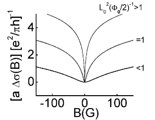
If spin effects are negligible , and the weak localization magnetoconductance is particularly simple.
| (2) |
A plot of Equation (2) at various temperatures is shown in Figure 4. In the figure, temperature is varied by varying , because the average inelastic dephasing length depends on temperature.
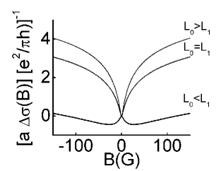
For most conductors, the spin-flip interaction is negligible (), and the terms proportional to can be safely neglected. The spin-orbit term, however, scales with the atomic number of the metal, . For light metals, such as lithium or magnesium, spin-orbit effects are negligible. For heavier metals, such as silver or gold, spin-orbit effects can dramatically alter the weak localization magnetoconductance signature.
Compared to the Drude conductivity, the weak-localization correction is very small. At most, the fractional correction to the conductivity, , is of the order
For a typical metal film with a thickness of Å, this is, approximately
In order to measure this magnetoconductance with an accuracy of , then, we would need to resolve changes in the total conductivity on the order of parts-per-million. This resolution demands good low-noise and small-signal detection methods, and teaching these methods is the purpose of this lab.
III Experimental apparatus
III.1 Samples and their preparation
The measurement electronics form the heart of this lab. Here, students learn techniques widely used in condensed matter labs for measuring very small signals in the presence of noise. In particular, they learn how to measure part-per-million changes in the resistance of a sample that will accept no more than a few milliamps of excitation current.
The first thing that our students do is make their thin film Ag samples. To make this easy for them, we have a rugged, home-built evaporative deposition (ED) system.
The technique of ED is simple enough so that most labs are in possession of the equipment needed to set up an ED system. The basic idea is to make a tightly sealed chamber and evacuate it, using vacuum pumps, so that the pressure is low enough for air molecules to be in the molecular flow regime (i.e. their mean free path is longer than the dimensions of the vacuum chamber). Under these conditions, ED can be performed by melting a Ag pellet. The resulting gas of Ag atoms will then travel to the walls of the chamber with a low probability of hitting air molecules. If a substrate is placed on one of the walls, it will then be possible to deposit a thin film of Ag onto this substrate. To meet the criteria of making the film quasi-2D (i.e. ), we find films need to be between 60-200Å thick. To make sure samples are that thin, our students use a commercially available thickness gaugeInfinicon to monitor the thickness of their films. So by using ED, thin film Ag samples can easily be made.
Once a sample is made, the students have to make contact to the film, cool it down, and make measurements in an applied magnetic field. In our lab, we use a commercially available liquid 4He dewar from Quantum DesignqdusaDewar , which comes with a 5 Tesla superconducting magnet, to cool the sample and make measurements in a magnetic field. This is not the only option though. The experiment can be done just as easily with an inexpensive dipping probe, inserted directly into a liquid 4He storage dewar. In fact, such a system would probably be preferable. The computer-controlled Quantum Design cryostat can sometimes obscure the physics of the experiment, and the central focus of the lab should be on the physics of electron transport in mesoscopic systems and techniques for low-level signal detection.
To prepare the samples for measurements, the students need to apply contacts to the film, and they need to have electrical connections to the film when it is at liquid 4He temperatures (T). For our setup, students make contact from the sample to a resistivity sample stage, called a puckqdusaDC , available from Quantum Design. The contact is made using silver paste and gold wires. Once the contacts are made, the sample stage is loaded into the cold dewar, and we then provide a breakout box that allows connections to be made to the resistivity puck from inside the dewar.
At this point, the samples are ready to be cooled, and we need a way to measure the small magnetoconductance signal. To do this we use a resistive bridge technique, which we describe next.
III.2 Detection of magnetoresistance
The measurement electronics form the heart of this lab. Here, students learn techniques widely used in condensed matter labs for measuring very small signals in the presence of noise. In particular, they learn how to measure part-per-million changes in the resistance of a sample that will accept no more than a few milliamps of excitation current.
To relate the observable resistance change to the theoretical prediction for the change in conductivity, start with the relation between resistance and conductivity for a film of thickness , length , and width .
The change in resistance due to a change in conductivity is just
| (3) |
where we have defined as the resistance of a square film. Equations (1) and (2) give predictions for , which we will compare with measurements of .
To get and , we simply pass a small excitation current through the sample and then measure the resulting voltage across the sample. This gives us the total resistance of the sample , and from that we can calculate , provided we know the sample’s length and and width .
Measuring the magnetoresistance is done in a similar way, but because is so much smaller than the “background” signal , we need an extra trick: nulling. What we are really measuring, remember, is the voltage across the sample produced by the excitation current , or .
If we can produce a reference voltage that is equal to the zero-field voltage across the sample, , then we can subtract this from the actual voltage across the sample to get .
| (4) |
This very small signal can then be amplified and examined in detail as a function of magnetic field H.
This process of nulling will only work if we can produce a small voltage that is independent of the magnetic field. Fortunately, this is easy to do using a passive, adjustable, low noise voltage divider. We used a Dekatran DT72A tunable voltage divider,Deka driven by the same voltage that produced the excitation current for the sample.
In both the and measurements, it is important not to use the same set of wires to carry the excitation current and to measure the resulting voltage across the sample. Long wires leading down into the cryostat may have resistances of their own which, if their leads carry current, will produce voltages that have nothing to do with the sample. In order to measure only that voltage produced by the sample, we employ a four-wire geometry, as shown in Figure 5.
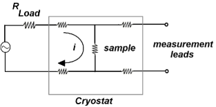
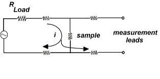
For this four-wire technique to be effective, no current must be allowed to flow along the measurement leads. If it did, a spurious voltage would be produced from the resistances in the measurement leads, and this would contaminate the measurement. Such a condition can result, for example, from the measurement device and the excitation source sharing a common ground, as shown in Figure 6. This condition is known as a ground loop, and care is needed to avoid it.
All of these measurements are performed at audio frequencies using a lock-in, which the students have been introduced to in a previous lab.Ph77LockIn We add to their training with a lock-in by encouraging them to analyze the noise in each component of their apparatus and in the apparatus as a whole. This is easily done with a lock-in by terminating the input of a device with a terminator and then measuring the noise of the output signal on the lock-in. The students can then determine which component is setting their noise floor; our students find the pre-amplifier sets their noise floor.
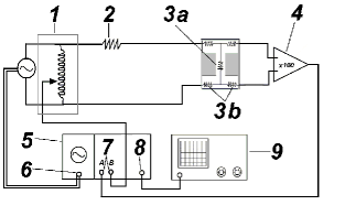
Lock-in detection, nulling, four-wire measurements, and ground loops are all essential topics for modern, condensed matter experimentalists to be familiar with, and these labs together provide students with a thorough, quantitative, foundation in each. A brief schematic of our entire apparatus for performing these functions is in Figure 7.
IV Typical Results
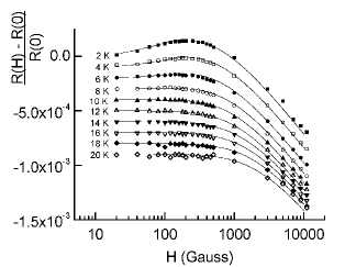
Using the techniques described above, our students found results consistent with weak localization. Their results are shown in Figures 8 and 9.
Figure 8 shows typical magnetoresistive data and fits to the data. The results clearly show weak localization with spin effects at low temperatures (T), as evidenced by the initially positive magnetoresistance at low magnetic fields followed by negative magnetoresistance at higher field values. This feature can be completely described using Equation (3) to convert Equation (1) to a magnetoresistance prediction, as described previously, and then fitting the data. The switch from positive to negative magnetoresistance represents a competition between the positive magnetoresistance, due to spin effects, and the decoherence of weak localization due to the magnetic field, which produces a negative magnetoresistive effect. At high enough magnetic fields, the decoherence wins out over the positive magnetoresistance, and the sign of the magnetoresistance changes.
At T14K and above, Equation (1) and (2) can both be used to describe the magnetoresistance (after being converted using Equation (3)). This reflects the fact that spin effects are irrelevant when phonon scattering is much more frequent that spin-orbit scattering of electrons, which is the case at higher temperatures (T). AboveT, , and if we set in Equation (1), then we get Equation (2). What this means is that we have thermally decohered the interference effects due to spin-orbit scattering by exciting phonons.
To fit the data in Figure 8 for all temperatures, the students performed a two parameter fit of Equation (1) converted into magnetoresistive form by Equation (3). This required the parameters, and , to be adjusted until a good fit was made. We encouraged the students to fit the equations visually until the fits were close, which was useful because it required the students to think about the relevant length scales of and and what they meant. is the average length that an electron travels before undergoing an inelastic scattering event with a phonon. , on the other hand, is a parameter that describes whether electrons scatter more frequently from phonons or from disorder, via spin-orbit scattering. Their values of and for the fits in Figure 8 are shown in Figure 9, as a function of temperature.
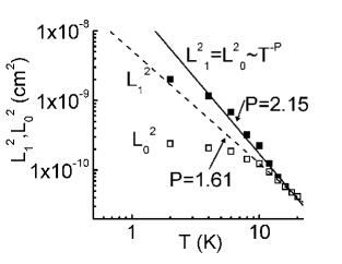
The typical length scale for and is about , and at low temperatures (T), . This indicates that spin-orbit scattering is more frequent than phonon scattering at low temperatures, as we expect. This is the reason weak localization, with spin effects, is observed.
Above 14K (as shown in Figure 9), , and we notice that the log-log plot of and squared versus temperature has a slope between -1.61 and -2.15. In an experimental paper with similar results to ours, Gershenzonref:gersh points out that the slope of and squared versus temperature, on a log-log plot, should be equal to -2 if we expect 2D thermal phonons to be the source of inelastic scattering. So above 14K, our students are likely observing 2D thermal phonon modes being excited and causing localization effects to die away.
V Conclusions
Our experiment on weak localization provides an introduction to modern experimental condensed matter research. The lab illustrates many of the experimental techniques that are used in modern research labs. Students learn to make their own samples, make contact to them, cool them down, and then make measurements. In addition, the resistance bridge technique considered here is a common technique to observe small signals on top of a large background signal.
The typical results from our students indicate that our technique is able to observe the predicted macroscopic expression of weak localization through the magnetoresistance of Ag thin films. Their results also show that at easily accessible temperatures the effect is clear to resolve.
In conclusion, the lab serves as a good transition from cookbook type labs to the real research environment.
VI Acknowledgments
This work was supported by the National Science Foundation under grant number DUE-0088658.
References
- (1)
References
- (1) Paul Drude, “Zur elektronentheori der metalles 1 Teil,”Ann. Phys. 1, 566–613 (1900); ”Zur elektronentheori der metalles 2 Teil, Galvanomagnetische und thermomagnetisch effecte,” Ann. Phys. 3, 369–402 (1900).
- (2) Gerd Bergmann, “Weak Localization in Thin Films: a time-of-flight experiment with conduction electrons,”Phys. Rep. 107, 1–58 (1984).
- (3) Sudip Chakravarty and Albert Schmid, “Weak localization” The quasiclassical theory of electrons in a random potential,”Phys. Rep 140, 193–236 (1986).
- (4) XTC/C: Thin Film Deposition Controller. Infinicon, Two Technology Place. East Syracuse, NY 13057-9741.
- (5) Physical Property Measurement System. Quantum Design, Inc. San Deigo, CA.
- (6) DC resistivity puck. Quantum Design, Inc. San Diego, CA.
- (7) Dekatran DT72A. Tegam, Ten Tegam Way, Geneva, OH 44041.
- (8) K.G. Libbrecht, E.D. Black, and C.M. Hirata, “A Basic Lock-in Amplifier Experiment for the Undergraduate Laboratory,”Am. J. Phys. 71 1208–1213 (2003).
- (9) M.E.Gershenzon, V.N. Gubankov, and Yu. E. Zhuravlev, ““Weak” localization and electron scattering in silver thin films,” JETP Lett. 35, 576–580 (1982).