, , , , , , , , , , , , , , , , , , , ,
A Hadron Blind Detector for the PHENIX Experiment at RHIC.
Abstract
A Hadron Blind Detector (HBD) is being developed for the PHENIX experiment at RHIC. It consists of a Čerenkov radiator operated with pure CF4 directly coupled in a windowless configuration to a triple-GEM detector element with a CsI photocathode and pad readout. The HBD operates in the bandwidth 6-11.5 eV (110-200 nm). We studied the detector response to minimum ionizing particles and to electrons. We present measurements of the CsI quantum efficiency, which are in very good agreement with previously published results over the bandwidth 6-8.3 eV and extend them up to 10.3 eV. Discharge probability and aging studies of the GEMs and the CsI photocathode in pure CF4 are presented.
keywords:
HBD , GEM , CsI photocathode , UV-photon detector , CF4PACS:
29.40.-n , 29.40.Cs , 29.40.Ka , 25.75.-q1 Introduction
We describe the operation and performance of a Hadron Blind Detector (HBD) which is being developed as an upgrade of the PHENIX detector at the Relativistic Heavy Ion Collider (RHIC) at BNL. The main purpose of the HBD is to allow the measurement of low-mass ( 1 GeV/c2) electron-positron pairs produced in central heavy ions collisions at energies up to = 200 GeV. Low-mass dileptons are a powerful observable in the quest for the quark-gluon plasma and in particular for the restoration of chiral symmetry expected to take place in ultra-relativistic nuclear collisions. The results of the CERES experiment [1] at CERN support the unique physics potential of this probe. The strong enhancement of low-mass pairs observed in nuclear collisions could only be explained by invoking the annihilation channel with an in-medium modification of the intermediate meson which could be linked to the restoration of chiral symmetry [2].
With its excellent mass resolution, the PHENIX detector has the potential to perform precision spectroscopy of the , , and mesons in addition to the pair continuum measurement. The observation of mass shifts of the , and mesons would provide direct evidence for the scenarios invoking the restoration of chiral symmetry. However, the present configuration of the PHENIX detector is severely limited in the low-mass region. The detector lacks the capability to recognize and reject the overwhelming yield of combinatorial background pairs, i.e. uncorrelated pairs formed by tracks from unrecognized conversions and Dalitz decays. In the mass range 0.3 - 0.5 GeV/c2 the present signal to background ratio is S/B 1/300, making the measurement of the low-mass pair continuum practically impossible.
An upgrade of the PHENIX detector is therefore necessary for this measurement. The present work is focussed on the development of an HBD which is the key element for such an upgrade. The HBD consists of a Čerenkov radiator, operated with pure CF4 and directly coupled to a triple Gas Electron Multiplier (GEM) [3] photon detector element [4, 5]. The concept is described in detail in Section 2.
In a recent publication [4] we have demonstrated the successful operation of a triple-GEM detector in pure CF4. In particular we have shown that the detector operates in a stable manner at gains up to 104 with and without a reflective CsI photocathode evaporated on the upper face of the top GEM. In the present paper, we concentrate on the hadron blindness properties and performance of the HBD. We present results obtained with a Hg UV lamp, a 55Fe X-ray source and an 241Am alpha source. We also present results from beam tests carried out at KEK using 1 GeV/c pions. Section 3 describes the various setups and conditions under which the measurements were performed. Section 4 presents measurements of the detector response to photoelectrons, alpha particles and pions as a function of the drift field. In Section 5, we present our measurements of the CsI quantum efficiency over the bandwidth 6-10.3 eV. The discharge probabilities of HV-segmented GEM foils are discussed in Section 6 and aging studies of the GEM foils and the CsI photocathode in pure CF4 atmosphere are presented in Section 7. A short summary and conclusions are presented at the end of the paper, in Section 8.
2 The HBD concept.
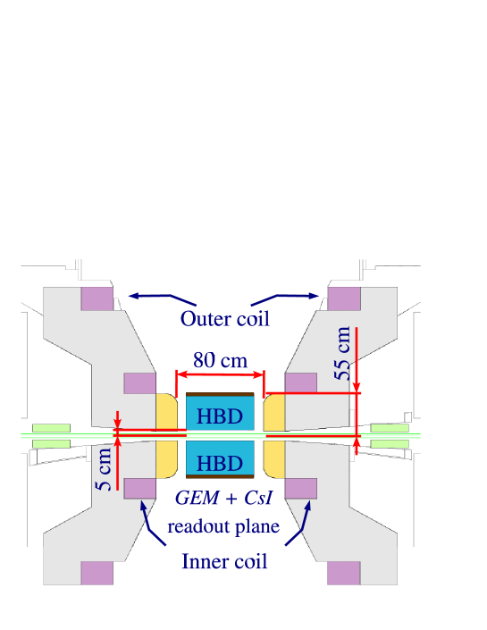
The PHENIX detector was designed anticipating that the measurement of low-mass pairs would be feasible with an appropriate upgrade. In particular, provision was made for the installation of an inner coil which would create an almost field-free region close to the vertex, extending out to 50-60 cm in the radial direction. In addition to this coil, the second major element of the upgrade is an HBD located in this field free region. The main task of the HBD is to recognize and reject conversions and Dalitz decay pairs by exploiting their small opening angle. Its size is constrained by the available space starting outside the beam pipe (at r5 cm) and ending before the inner coil (at r55 cm). Fig. 1 shows the layout of the inner part of the PHENIX detector together with the location of the coils and the proposed HBD.
The system specifications of the HBD have been extensively studied in Monte Carlo simulations. [6]. A reduction of the combinatorial background originating from conversions and Dalitz decays of at least two orders of magnitude can be achieved with a detector that provides electron identification with a very high efficiency, of at least 90%. This also implies a double (electron) hit recognition at a comparable level. On the other hand, a moderate rejection factor of 100 is sufficient. Possible realizations of the HBD detector were considered in the study. After careful consideration of relevant options for the key elements (gases, detector configuration and readout chambers), the choice that emerged is a windowless Čerenkov detector, operated with pure CF4 in a proximity focus configuration, with a CsI photocathode and a triple-GEM detector element with pad readout.
Since a mirror-type RICH detector in the center of PHENIX is very difficult or nearly impossible to implement, we consider a scheme without mirror and without window in which the Čerenkov light from particles passing through the radiator is directly collected on a CsI photosensitive cathode plane, forming a circular blob image rather than a ring as in a RICH detector. The choice of CF4 both as radiator and detector gas in a windowless geometry results in a very large bandwidth (from 6 eV given by the threshold of the CsI to 11.5 eV given by the CF4 cut-off) and consequently in a very large figure of merit N0 and a very large number of photoelectrons Npe that was estimated to be of the order of 40 in a 50 cm long radiator [6]. This large number of photoelectrons ensures a very high electron efficiency, and more importantly, it is crucial for achieving a double-hit recognition larger than 90%.
Another important advantage of the present design using GEMs is that it allows the use of a reflective photocathode (i.e. the top face of the first GEM is coated with a thin layer of CsI and the photoelectrons are pulled into the holes of the GEM by their strong electric field) and consequently the photocathode is totally screened from photons produced in the avalanche process.
The present readout scheme foresees the detection of the Čerenkov photoelectrons in a pad plane with hexagonal pads of size slightly smaller than the blob size (10 cm2) such that the probability of a single pad hit by an electron entering the HBD is negligibly small. This results in a low granularity detector. In addition, since the photoelectrons produced by a single electron will be distributed between at most three pads, one can expect a primary charge of at least 10 electrons/pad, allowing operation of the detector at a relatively moderate gain of a few times 103.
3 Setup and experimental conditions.
GEMs produced at CERN were used in all measurements. The GEMs were made of 50 m kapton foils with 5 m thick copper layers, 60-80 m diameter holes and 140 m pitch. They had a sensitive area of 3030 mm2 or 100100 mm2. These two types of GEMs will be referred to in the text as ”small” and ”large” respectively. The top side of some of the large GEMs was divided into four segments (25100 mm2 each) and will be referred to in the text as ”segmented”. 3 GEMs were assembled into one stack with G10 frames as shown in Fig. 2. The distance between the drift mesh and the top GEM (GEM1), the distance between GEMs and the distance between the bottom GEM (GEM3) and the printed circuit board (PCB) were all equal to 1.5 mm. The PCB consisted of 9 square pads of size 3333 mm2. Each pad was connected to a charge sensitive preamplifier. CF4 with 99.999% purity was used in all measurements.
In most tests, the high voltage to the GEMs and mesh was supplied by a single HV power supply through a three-branch resistive chain (Fig. 2). In this scheme three independent resistive dividers provide the voltage to the top and bottom planes of each GEM. When a discharge occurs in one GEM the voltage across the other GEMs drops only slightly unlike the case of a single-branch resistive divider. In the latter case the voltages across other GEMs increase and can cause multiple discharges and damage the GEMs. The resistors R in the chain were 5.6 M, R1 and R2 were 1.2 M. For the segmented GEMs, the resistors R2 were connected directly to each segment and were located inside the detector box. To ensure almost 100% electron collection efficiency to the PCB, the induction field EI is set to twice the transfer field ET [4]. For the measurements where the drift field was varied, two HV power supplies were used, one for the mesh and one for the three GEMs.
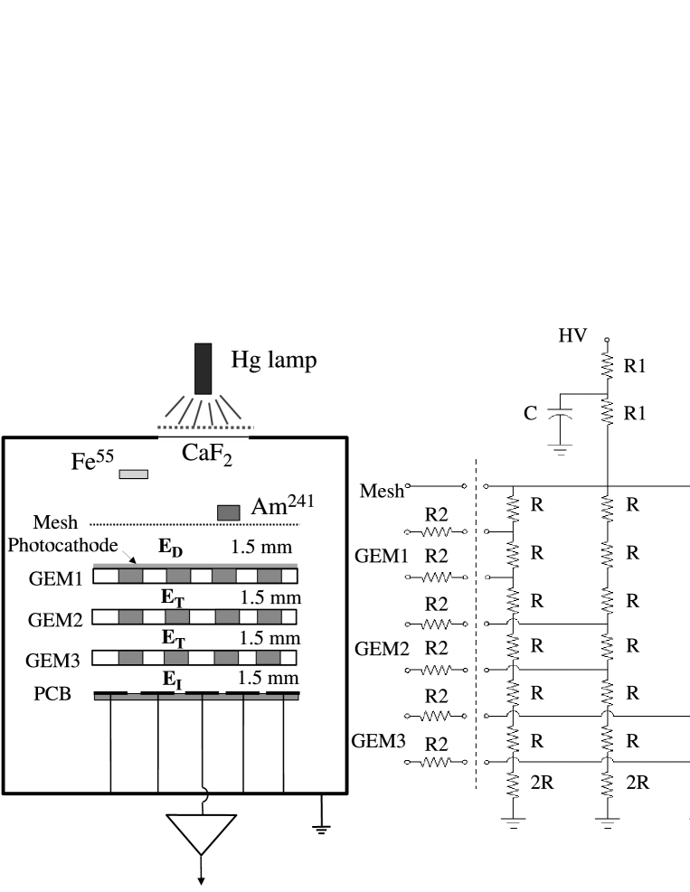
For the measurements with the reflective CsI photocathode GEM1 was prepared with a gold-coated surface to prevent chemical interaction with cupper. Below the gold layer a thin Ni layer was deposited in order to provide good adhesion of the gold layer. The gold-coated GEMs were also produced at CERN and the deposition of the CsI layer was performed at the Radiation Detection Physics Laboratory at the Weizmann Institute. The thickness of the CsI layer was kept to 2000 . For the operation with the reflective photocathode the drift field is set to be equal to zero or even slightly reversed in order to collect only the photo-electrons from the CsI layer and to repel the ionization of minimum ionizing particles. For these measurements the corresponding contact of the resistive chain was disconnected and an independent power supply was used for the mesh.
The GEMs, PCB and drift mesh were mounted inside a stainless steel box which could be pumped down to 10-6 Torr and was connected to inlet and outlet gas lines to allow gas flushing. The setup contained also devices for the precise measurements of temperature, pressure and water content down to the ppm level. For the tests with 55Fe X-rays, the radioactive source was positioned on a moving arm inside the box at a distance of 40 mm from the mesh. The 55Fe source could be moved out of the sensitive volume. The total rate of X-rays was kept at the level of 1 kHz. The 5.9 keV photons from 55Fe release 110 electrons in CF4 (54 eV per electron-ion pair). For the measurements of the discharge limits with heavily ionizing particles we used an 241Am source which emits 5.5 MeV alpha-particles. The source was attached to a moving arm that could be inserted at a distance of 1mm from the mesh and was strongly collimated in order to provide high energy deposition and small energy dispersion in the sensitive gap. The rate of alpha-particles was 100 Hz.
The measurements with the CsI reflective photocathode were performed with a Hg-lamp through a UV-transparent CaF2 window mounted on the cover of the detector box. The lamp was positioned above the window with an absorber which reduced the UV flux by about a factor of 1000 in order to prevent damage to the photocathode. The illuminated area of the detector was about 1 cm2. In this geometry the measured photo-electron current was about 2106 electrons/mms.
The study of the gain limits required a reliable way to monitor discharges in the triple-GEM assembly via the resistive chain. The chain was biased by a CAEN-126 HV-power supply. This module includes protection against over-current with a precision of 0.1 A. The current in the resistive chain was in the range between 250 and 300 A and the protection threshold was always kept at 1 A above the normal value. This was enough to cause a trip when a discharge occurred in a GEM. The trip signal was reset after 1 second and was also counted by a scaler.
The beam test at KEK was done with a 1 GeV/c secondary beam of negative particles (mainly pions) containing a few percent of electrons. The setup consisted of two gas Čerenkov counters (GCC), a set of scintillation counters (S1, S2 and S3), the HBD and a lead glass calorimeter (PbGl). The HBD consisted of a 50 cm long radiator directly coupled to the detector box and setup described above. The detector was operated with pure CF4 at a relatively high rate of 100 Hz/cm2 and at a gain of . S1 (10045 mm2) was in front of the two GCC’s, S2 (2510 mm2) was just in front of the HBD and S3 (5045 mm2) was behind the HBD and in front of the PbGl calorimeter. The trigger was defined by a coincidence between the three scintillation counters S1S2S3. Pions and electrons were selected offline using the data from the two GCCs, the PbGl and the time-of-flight measured between S3 and S1.
4 Detector response as function of the drift field.
A hadron blind detector is characterized by its insensitivity to hadrons, i.e. by a large hadron rejection factor while keeping a high detection efficiency for electrons. The hadron blindness property of the proposed detector is achieved by reversing the direction of the drift field ED thereby pushing most of the ionization charges towards the mesh. With this negative drift-field configuration, photoelectrons released from the CsI photocathode surface are still effectively collected into the GEM holes due to the strong electric field inside the holes which is typically of the order of 100 kV/cm.
In order to characterize and quantify both the hadron rejection factor and the photo-electron detection efficiency, we performed systematic measurements as a function of the drift field with alpha particles, pions of 1 GeV/c and UV photons. Details of these measurements and the results are presented in this section.
4.1 Detector response to minimum ionizing particles and alpha particles.
Fig. 3 shows the pulse-height distribution, after pedestal subtraction, measured at KEK with 1 GeV/c pions for various values of ED. The signal is expressed in terms of the primary ionization charge, using the 55Fe spectrum measured under identical conditions. For ED = +1 kV/cm, the measured mean amplitude is 18 e corresponding to a primary ionization of 120 charges/cm or 54 eV/ion-pair assuming an energy loss of dE/dx = 7 keV/cm [7]. The spectrum is well reproduced by a Landau distribution characteristic of the energy loss of a minimum ionizing particle (mip).
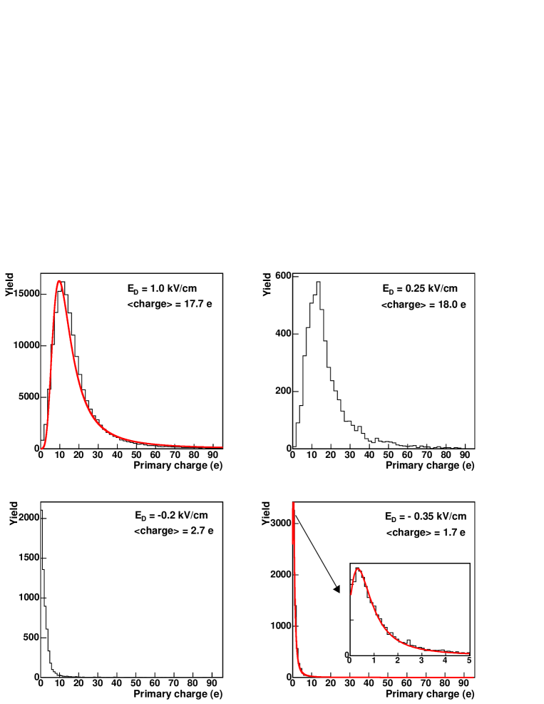
The spectrum remains practically unchanged as long as ED is positive as shown for two cases in the upper panels of Fig. 3. As soon as ED is reversed, i.e set to negative values, there is a sharp drop in the pulse height as the primary charges get repelled towards the mesh. The mean amplitude drops to 10% of its value for a positive field. This value results from the collection of ionization charges (i) from a thin layer above the first GEM surface and (ii) from the entire first transfer gap which are subject to a two-stage amplification. At a gain of 104, the former is estimated to be a factor of 2 larger than the latter, indicating that when the drift is reversed, ionization charges are collected from a layer of above the first GEM.
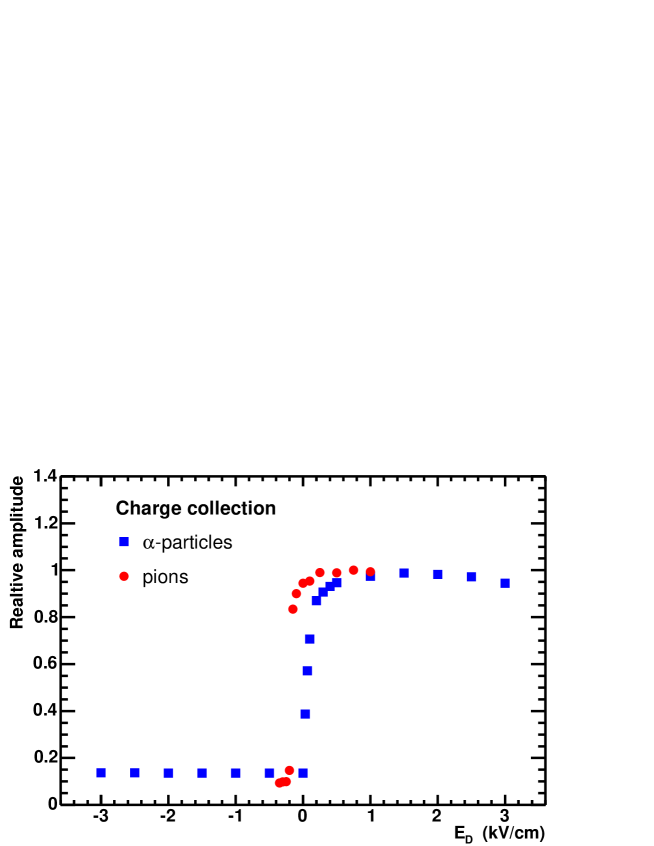
The mean amplitude vs. ED is shown in Fig. 4. The amplitude decreases sharply when the polarity of the drift field is switched and this occurs within a ED range of 0.1 kV/cm. The figure shows also the results of similar measurements performed with alpha particles. The results are practically identical in both cases. The small difference in the values of the field at the onset of the signal drop is well within the uncertainties of the absolute high-voltage values given the power supplies used in the two measurements.
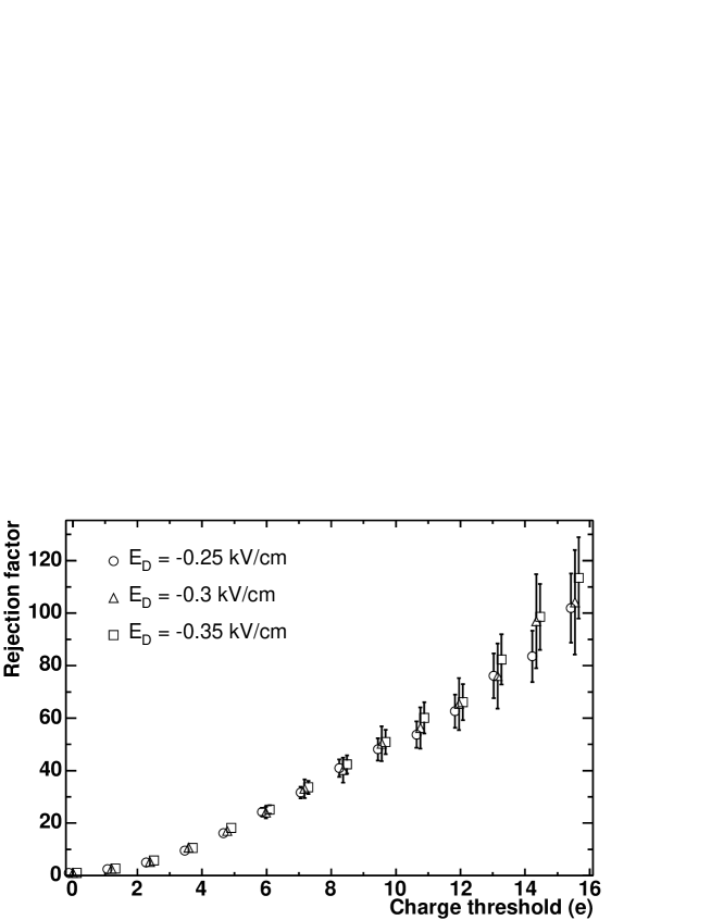
The hadron rejection factor derived from the pion spectra measured at negative drift fields is shown in Fig. 5. The rejection is limited by the long Landau tail and depends on the amplitude threshold that can safely be applied without compromising the electron collection efficiency. Rejection factors of the order of 50 can be achieved with an amplitude threshold of 10 e. A much higher rejection factor is achieved by combining the amplitude response with the hit size. As mentioned above, the pad readout consists of hexagonal pads with a size somewhat smaller than the Cherenkov blob size. Under these conditions charged particles will produce single pad hits whereas electrons will most probably produce multiple-pad hits thereby providing an additional powerful handle on the charged particle rejection.
4.2 Detector response to photoelectrons.
Measurements as a function of the drift field to determine the electron detection efficiency were performed with UV-photons from a Hg lamp irradiating the CsI photocathode through the UV-transparent CaF2 window. We measured the photo-current at the PCB for values of the HV accross the GEMs varying from 442 to 506 V which correspond to gas gain variations of more than a factor of 40. The results are shown in Fig. 6. The various measurements have been normalized to 1 at ED=0 kV/cm to represent the relative detection efficiency and to allow an easy comparison between the measurements. The relative detection efficiency is practically independent of the field
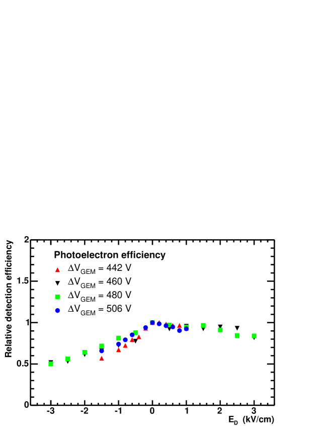
across the GEMs. The efficiency slightly increases as the positive drift field decreases, reaching a maximum at 0 kV/cm. A mild decrease in the current is then observed as the drift field becomes more and more negative demonstrating that the detection efficiency of the photoelectrons remains very high even at negative drift fields of 1 kV/cm. Combining the results of Figs. 4 and 6 one sees that the best performance is achieved by applying a slightly negative field in the drift gap. The results presented here are consistent with those of ref. [8, 9] though with different gases and voltages across the GEMs.
5 CsI Quantum Efficiency
The absolute quantum efficiency (QE) of the CsI photocathode was measured by a large number of groups (see [9], [10] for comprehensive reviews and further references). Most of the measurements are in reasonable agreement with each other. However, none of these measurements were performed at wavelengths below 150 nm (or a photon energy above 8.3 eV). Since CF4 is transparent up to 11.5 eV it was important to extend the measurements of the absolute QE of CsI as much as possible.
The determination of the absolute QE requires an absolutely calibrated light source, which is not available in most laboratories. Therefore, usually a relative method is used, namely the recording of the sample response relative to a ”known” reference. In our measurements we used as a reference a calibrated photomultiplier tube.
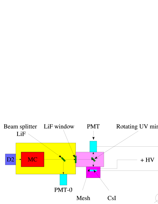
The experimental setup used for the determination of the absolute quantum efficiency of the CsI layer is shown in Fig. 7. It includes a vacuum ultraviolet (VUV) monochromator (Jobin Yvon H20, 115-500 nm) equipped with a deuterium lamp (Hamamatsu L7293, 115-320 nm), coupled via a LiF window (cut-off at 105 nm) to a detector box. The monochromator box also includes a LiF beam splitter which splits the beam between the photomultiplier PMT-0 (Hamamatsu R1460) and the detector box. PMT-0 serves as a normalization to monitor the deuterium lamp intensity. The detector box included an absolutely calibrated photomultiplier tube PMT (Hamamatsu R6836) on one side and on the other side a box containing a small (33 cm2) GEM foil on which a 2500 layer of CsI was evaporated. PMT was operated in photodiode mode (gain=1). Above the foil and at a distance of 1.5 mm from it was a mesh electrode which was at a positive voltage with respect to the foil. The detector box also had a UV mirror which served to deflect the beam alternatively to the CsI layer and to the PMT. Collimators of 8 mm diameter were placed in front of the mesh and PMT, making sure that the solid angle seen by the photomultiplier and the CsI layer was exactly the same. By rotating the UV-mirror the current was measured in turn over the whole wavelength range on both devices.
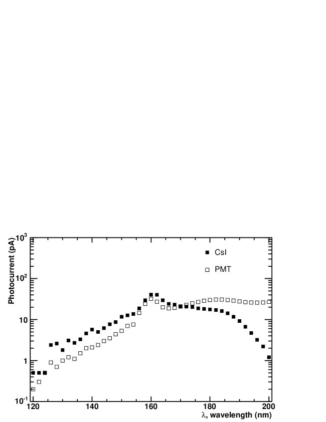
The current of the CsI and photomultiplier PMT as measured in vacuum is shown in Fig. 8. The measurements were done over the wavelength range of 120 - 200 nm (E = 6.2 - 10.3 eV). The measurements were repeated with gas at atmospheric pressure. The total path in CF4 was 23 cm.
The absolute quantum efficiency of the CsI layer at a given wavelength is given by:
| (1) |
where is the absolute quantum efficiency of the PMT at the wavelength , - the CsI photocathode current measured at that wavelength, - the PMT photomultiplier current at , - the mesh transparency ( = 0.81), and - the opacity of the CsI layer due to the GEM holes ( = 0.833).
Fig. 9 shows the CsI absolute quantum efficiency in vacuum and plotted as a function of the photon energy. (Plotting the quantum efficiency as a function of photon energy has the advantage that the figure of merit N0 is simply given by the area under the points). The present results are in very good agreement with those of ref [9] which covered the range 6-8.3 eV.
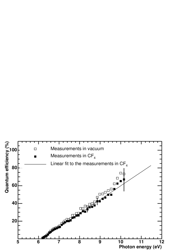
The range of the measurements shown in Figs. 8 and 9 (120 - 200 nm, or 6.2 -10.3 eV) was limited by the light intensity of the deuterium UV lamp at 10.3 eV. Over this bandwidth we derive a figure of merit N0 of 459 cm-1 (414 cm-1) or an average QE value of 31% (28%) in vacuum (CF4). However the useful range of UV photons in the HBD extends up to the CF4 cut-off which is at 11.5 eV. Extrapolating the data of Fig. 9 to 11.5 eV under the assumption of a linear dependence of the quantum efficiency vs. photon energy gives a figure of merit N0= 822 cm-1 or an average quantum efficiency of 55% in CF4. For a 50 cm long radiator this N0 value would correspond to 35 photoelectrons (p.e.) (after taking into account the losses due to the entrance mesh and the holes of the top GEM). This unprecedented value of N0 is a direct consequence of the large bandwidth of CF4 in the present windowless configuration111A direct measurement of N0 during the beam test at KEK was not possible due to the large UV absorption in the available gas system. We observed only 6-10 p.e. per electron trigger. This number is however consistent with the expected number of 35 p.e. after correcting it for the measured absorption in the gas..
6 Discharge probability and saturation effect.
Stability of operation and absence of discharges in the presence of heavily ionizing particles is crucial for the operation of the HBD. The 241Am source was used to simulate heavily ionizing particles under laboratory conditions. In our earlier paper [4] the discharge probability was measured in small GEMs. In Ar/CO2 it was found to increase sharply at a gas gain of 2104 when the total charge approached the Raether limit of 108 [11] whereas in CF4 no such sharp increase was found. On the contrary the onset of the discharges was spread over a broad gain range (see Fig. 4 in [4]). The robustness of CF4 against discharges compared to Ar/CO2 was attributed to the charge saturation observed in CF4 at the level of 2107 e (i.e. below the Raether limit). However, all the measurements in CF4 were done with 3030 mm2 GEMs. Similar measurements on large GEMs could not be done since the first spark usually destroyed one of the GEMs due to the large energy stored in the large capacitance.
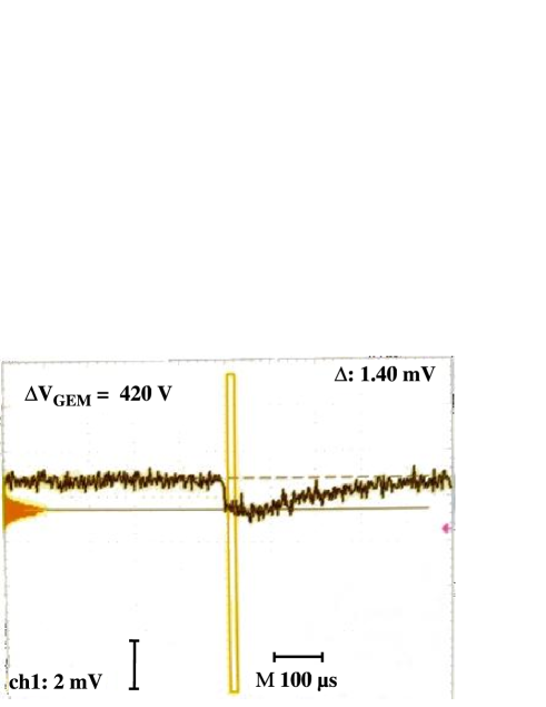
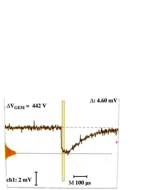
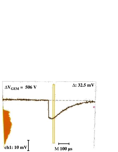
In the present work we used HV segmented 100100 mm2 GEMs to repeat the discharge probability studies and revisit the charge saturation effect in a more careful way. In particular, at high values of the total charge, when the pre-amplifier is close to saturation, the output signal is already reduced compared to its real value. We therefore repeated the measurements of the total charge produced by alpha-particles as a function of the GEM voltage without any pre-amplifier, with the central pad directly connected to the 1 M input of an oscilloscope through a 1m coaxial cable. In this case the pulse height observed at the scope is determined by the ratio of the charge induced in the pad and the total capacitance of the pad including the capacitance of the cable. Examples of the pulses and pulse-height distributions measured with this method are shown in Fig. 10. In the figures the screen images of the oscilloscope are shown together with the pulse height distribution on the left side of the figures. The three figures correspond to 3 different voltages on the GEMs. The risetime of the pulses is determined by the induction of charge by the moving electrons and the decay time is determined by the RC constant of the readout chain, i.e. the product of the pad capacitance and the impedance of the scope (1 M). In Fig. 11 we compare the signal measured without pre-amplifier at the 1 M input of the oscilloscope and the measurement with pre-amplifier. Both measurements were performed under identical conditions and for this purpose the pre-amplifier was calibrated in units of input charge. In order to obtain the relation beween the signal measured without pre-amplifier and the input charge the results were normalized in the range VGEM = 420 - 440 V where both measurements could be performed and the amplifier was still far from saturation. At V 490 V the pulse-height resolution deteriorates considerably and we therefore plot the mean value (instead of the peak value) of the pulse-height distribution.
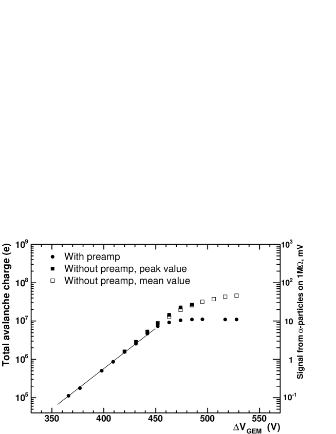
Fig. 11 shows clearly that the signal from alpha-particles deviates from the exponential dependence when the total charge exceeds the value of 107 electrons. The signal measured with the pre-amplifier is saturated at the level of 107 e (in the measurements described in [4] a pre-amplifier with higher saturation level was used). The signal measured without the pre-amplifier saturates at about 4107 e. The bottom panel of Fig. 10 was obtained at VGEM = 506 V where according to Fig. 11 the saturation effect is already quite pronounced (the mean signal is suppressed by almost a factor of 3 with respect to the expected exponential behaviour) establishing a clear correlation between the saturation effect and the deterioration of the pulse height resolution.
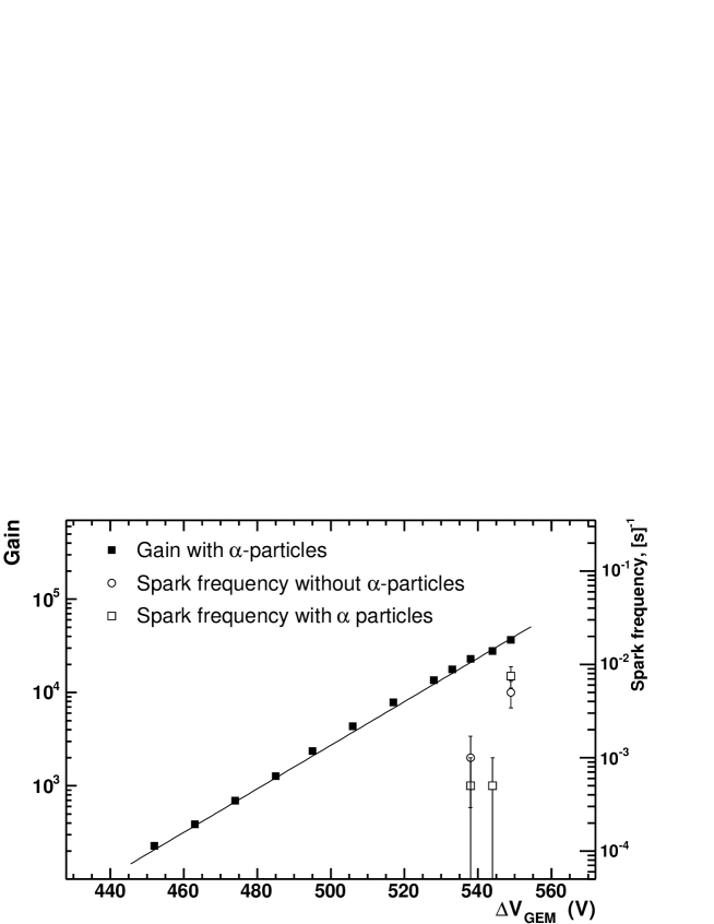
As already mentioned the saturation of the signal strongly suppresses the probability of the discharges provoked by heavily ionizing particles. This suppression was also observed in the measurements of the discharge limits performed with the segmented large triple-GEM detector. The results of these measurements are shown in Fig. 12. Two measurements are presented in the figure, the measurement in the presence of alpha-particles and the measurement without alpha-particles. In both cases the gain was monitored at each voltage with the 55Fe source. The dependence of the gain on voltage is presented in the figure together with the spark frequency as a function of the GEM voltage. The duration of each measurement was 2000 s, i.e. the maximum number of sparks counted in the highest point was about 20. The present detector showed negligible spark probability at gains up to . The results demonstrate that the discharge limit does not depend on the presence of alpha-particles in the sensitive volume of the detector. Rather it seems that only local defects in the GEMs are responsible for the discharges and limit the gain of the device.
During the series of tests the detector experienced a total number of 40 sparks but no sign of any degradation was observed in its performance and all three GEMs were still fully operational at the end of the test.
7 Aging studies.
In the present HBD two possible sources of long term detector degradation under irradiation can be identified: aging of the CsI photocathode due to ion back-flow and possible chemical reactions with active radicals formed in electron-ion avalanches in CF4, and aging of the GEMs due to etching of metal or insulator surfaces and/or polymerization of pollutants from avalanches in CF4 at the metal or insulator surfaces. Both processes depend on the total charge flowing through the detector which is the product of the photo-electron current collected into the holes of the first GEM and the total gain of the triple-GEM system.
Assuming operation at a gain of we conservatively estimate the total charge flow through the HBD in normal PHENIX operation to be 10-20 C/cm2/year. Thus we decided to perform an aging test of the detector module up to an accumulated total charge of 100 to 200 C/cm2 to represent approximately ten years of HBD operation in PHENIX.
The aging tests were performed so as to decouple the degradation of the photocathode from the deterioration of GEMs. We used two sources of radiation: The UV Hg-lamp and the 55Fe X-ray source. The UV lamp was used for continuous irradiation of the detector under test and the current to the PCB was monitored. Every few hours the UV irradiation was stopped and the 55Fe source was inserted into the detector for a short gain monitoring allowing to assess the gain stability of the triple-GEM. Once the gain is known we can then infer the stability of the CsI photocathode. During UV irradiation the electric field in the drift gap was kept at zero whereas during the X-ray irradiation the drift field was set to 1 kV/cm.
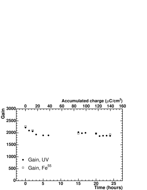

In Fig. 13 the results of two aging tests are shown. The first test (Fig. 13, left) was performed with a small triple-GEM detector. The test took about 1 day and the total charge accumulated was 140 C/cm2. It is seen that the gain derived from the measurements of the current during UV-irradiation and the gain measured from 55Fe irradiation are very close to each other. After an initial gain drop of 10% in the first 20 hours, the performance was stable within 2%.
The second aging test was performed with a large segmented triple-GEM set. This test was done at a lower rate than the first one in that the detector accumulated a total charge of 150 C/cm2 in 4 days rather than in 1 day. As seen in the right panel of Fig. 13, the gain variations during the test did not exceed 20% and during the second half of the test they were even 5%. In the first 10 hours of irradiation the gain derived from UV irradiation and the one determined from the measurements with the 55Fe source differed by 20%. This result indicates that the photocathode efficiency or collection efficiency of the photo-electrons into the first GEM holes was higher during that period. After the first 10 hours both gains converged to the same value and followed a very similar dependence. The performance of both small and large GEM sets during the initial phases of the aging tests including the gradual increase of the gain in the second test is not yet understood222We have repeatedly observed gain variations during the initial operation of a triple-GEM over periods of time ranging from a few hours to a few days before stable operation was reached. The origin of these instabilities is unclear and will be the subject of further studies.. However as a result of these tests we conclude that both the photocathode efficiency and the GEM gain do not exhibit any dramatic change which can be interpreted as aging degradation of the detector.
8 Summary and conclusions
An HBD is being proposed for an upgrade of the PHENIX experiment at RHIC. The HBD is a windowless Čerenkov detector, operated with pure CF4 in a proximity focus configuration. The detector consists of a 50 cm long radiator directly coupled to a triple-GEM detector which has a CsI photocathode evaporated on the top face of the first GEM foil and a pad readout at the bottom of the GEM stack. We have studied the basic parameters which determine the HBD performance. In particular, we have presented results on the device response to mip’s and to electrons. Large hadron rejection factors, well in excess of 100, can be achieved while preserving an electron detection efficiency larger than 90%. Extrapolating the quantum efficiency of CsI from the measured range 6-10.3 eV to the expected operational bandwidth of the device (6-11.5 eV) gives a figure of merit N0=822 cm-1 and a very large number of photoelectrons of 36 over a 50 cm long radiator. The charge saturation effect occurring in CF4 when the total charge in the avalanche reaches 4107 e makes the HBD relatively robust against discharges. Our measurements show that the limit of stability is actually dictated by the quality of the GEM foils rather than by the presence of highly ionizing particles. Very stable operation can be achieved at gains up to 104 with 1010 cm2 GEMs segmented into four HV segments333Very stable operation at gains of 104 was also obtained with larger GEM foils of 2324 cm2 that we have tested recently.. Aging studies of the GEM foils as well as the CsI photocathode reveal that there is no significant deterioration of the detector for irradiation levels corresponding to 10 years of normal PHENIX operation at RHIC. Recently, a test was carried out of a triple-GEM detector operated with pure CF4 and located inside the PHENIX central arm spectrometer at a distance of 50 cm from the collision point [12]. The detector performed smoothly in the presence of Au+Au collisions exhibiting no discharges or gain instabilities. The measurements presented here and the beam test results demonstrate the validity of the proposed HBD concept and pave the way for the incorporation of such a detector in the PHENIX experiment.
Acknowledgements
We thank F.Sauli, A.Breskin, R.Chechik and M.Klin for their invaluable help and very useful discussions. This work was partially supported by the Israel Science Foundation, the MINERVA Foundation, the Nella and Leon Benoziyo Center for High Energy Physics Research and the US Department of Energy under Contract No. DE-AC0298CH10886.
References
- [1] G. Agakichiev et al., Phys. Rev. Lett. 75 (1995), 1272, Phys. Lett. B422 (1998), 405, and D. Adamova et al., Phys. Rev. Lett. 91 (2003), 042301,
- [2] G.E. Brown and M. Rho, Phys. Rep. 363 (2002), 85, and R. Rapp and J. Wambach, Adv. Nucl. Phys. 25 (2000), 1
- [3] F. Sauli, Nucl. Instr. and Meth. A386 (1997), 531.
- [4] A. Kozlov, I. Ravinovich, L. Shekhtman, Z. Fraenkel, M. Inuzuka and I. Tserruya, Nucl. Instr. and Meth. A523 (2004), 345.
- [5] D. Mörmann, A. Breskin, R. Chechik. C. Shalem, Nucl. Instr. and Meth. A530 (2004), 258.
- [6] Z. Fraenkel, B. Khachaturov, A. Kozlov, A. Milov, D. Mukhopadhyay, D. Pal, I. Ravinovich, I. Tserruya and S. Zhou, PHENIX Technical Note 391. http://www.phenix.bnl.gov/phenix/WWW/ forms/info/view.html.
- [7] D. Denisov, Nucl. Instr. and Meth. A306 (1991), 200.
- [8] D. Mörmann, A. Breskin, R. Chechik, P. Cwetanski and B.K. Singh, Nucl. Instr. and Meth. A478 (2002), 230.
- [9] D. Mörmann, A. Breskin, R. Chechik and B.K. Singh, Nucl. Instr. and Meth. A471 (2001), 333.
- [10] B.K. Singh, E. Shefer, A. Breskin, R. Chechik and N. Avraham, Nucl. Instr. and Meth. A454 (2000), 364.
- [11] H. Raether, Z. Phys. 112 (1939), 464.
- [12] B. Azmoon, N. Smirnov, S.P. Stoll and C.L. Woody, paper N16-49, IEEE, Rome 2004.