Bistable diode action in left-handed periodic structures
Abstract
We study nonlinear transmission of an asymmetric multilayer structure created by alternating slabs of two materials with positive and negative refractive index. We demonstrate that such a structure exhibits passive spatially nonreciprocal transmission of electromagnetic waves, the analogue of the electronic diode. We study the properties of this left-handed diode and confirm its highly nonreciprocal and bistable transmittance by employing direct simulations.
An all-optical diode is a spatially nonreciprocal device that allows unidirectional propagation of a signal at a given wavelength. In the ideal case, the diode transmission is 100% in the forward propagation, whereas it is much smaller or vanishes for backward (opposite) propagation, yielding a unitary contrast. The possibility of achieving highly nonreciprocal transmission through a passive, nonlinear device is not only novel and interesting concept, but also useful for many applications such as optical isolation and all-optical processing. Such unidirectional action was demonstrated for several asymmetric structures and different nonlinear materials Scalora et al. (1994); Tocci et al. (1995); Liang et al. (1997); Gallo and Assanto (1999); Mujumdar and Ramachandran (2001); Gawith et al. (2001); Gallo et al. (2001).
In this paper, we discuss a novel type of spatially nonreciprocal device based on an asymmetric multilayered structure created by alternating slabs of two materials, conventional and left-handed (LH), the latter is a material with both negative electric permittivity and negative magnetic permeability which results in an effective negative refractive index LHM . Such multilayered structures are a special class of structures consiting of a sequence of flat lenses that provide optical cancellation of the conventional, or right-handed (RH), layers leading to either enhanced or suppressed transmission Nefedov and Tretyakov (2002); Li et al. (2003); Feise et al. (2004a).
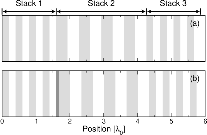
We employ a general idea to obtain diode action by making the structure both asymmetric and nonlinear. Also, we consider a periodic superlattice, which is expected to possess resonant properties, and thus enhancing nonlinear effects. We consider an asymmetric superlattice consisting of three stacks with four LH/RH double layers each [see Figs. 1(a,b)]. We assume that in the nonlinear regime, a dielectric defect layer with Kerr-type nonlinear response is inserted between stacks 1 and 2, as shown in Fig. 1(b). We study wave transmission in both linear and nonlinear regimes by using the transfer-matrix method (TMM) Yeh (1988), and also by employing direct numerical simulations based on the pseudospectral time-domain (PSTD) method Liu (1997). The transfer matrix of the system analytically relates the electromagnetic fields on either side of an element Yeh (1988). Complex structures can be build up out of simple elements through multiplication of the respective matrices. Thin nonlinear elements can be modelled, e.g., as delta-functions Lidorikis et al. (1998); Feise et al. (2004a).
In the PSTD method, the Maxwell equations are discretized in time and space. The spatial derivatives are approximated using discrete Fourier transforms and the temporal derivatives using central differences. From this, one derives update equations for the different fields and by iteration propagates the fields through time. The problem of the inherent periodicity of the Fourier transform can be removed through the use of perfectly-matched-layer absorbing boundary-conditions Liu (1997); Berenger (1994). The PSTD method samples all field components at the same location in the unit cell, which is advantageous when both the electric permittivity and the magnetic permeability vary with position Feise et al. (2004b). An instantaneous Kerr nonlinear material is included by directly solving the cubic equation for the intensity Tran (1996) at each iteration.
We model the LH material as having Lorentzian frequency dependence in both electric permittivity and magnetic permeability ,
| (1) | |||||
| (2) |
Here, are the corresponding plasma frequencies, are the resonance frequencies, and are absorption parameters. We use s-1, s-1, s-1, and include small losses, s-1. With these parameters, the refractive index of the LH material at frequency GHz, and the material is left-handed for frequencies GHz and right-handed for GHz. The RH layer is assumed to be air.
The structure shown in Fig. 1(a) consists of three stacks with four LH/RH double layers each. The outer stacks (Stack 1 and Stack 3) have individual layer thicknesses of , while the central stack (Stack 2) has individual layer thickness ; being the free-space wavelength of incoming radiation of the frequency . Figure 1(b) shows the same system with a structural defect introduced between Stack 1 and Stack 2. The defect layer has thickness .
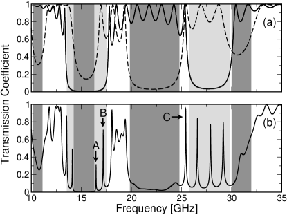
First, we study the transmission properties of the individual components of our superlattice in order to analyze the effect of the layer thickness on the positions of the band gaps and the transmission spectrum. Figure 2(a) shows the transmission spectrum of a structure made of the combination of Stack 1 and Stack 3 directly attached to each other (solid), as well as, the transmission spectrum of Stack 2 (dashed). The spectra show several transmission bands and gaps, and we clearly see a shift of the conventional band gaps due to the scaling of the structure. However, the band gap associated with vanishing average refractive index (around GHz) remains at the same frequency and only changes its width Li et al. (2003).
The transmission spectrum of the combined structure of Fig. 1(a) is shown in Fig. 2(b). In the frequency intervals where the central stack is opaque, the structure has a band gap, while at frequencies where the outer stacks are opaque but the central stack is transparent the structure behaves similar to a cavity resonator and shows the characteristic Fabry-Perot cavity peaks. In this system cavity-like behavior occurs in the frequency ranges of 13.5–14.3 GHz, 16.3–17.5 GHz, and 25.8–29.9 GHz.
To study the nonlinear transmission of our multi-stack structure, we introduce a defect layer with a linear electric permittivity , see Fig. 1(b). For the TMM calculations, we place a delta-function Kerr-type nonlinearity at the left interface of the defect layer Lidorikis et al. (1998) , , while in the PSTD calculations the entire defect layer has a nonlinear electric permittivity , with the nonlinearity coefficient . We study the difference in transmission when the light is incident from opposite sides of the structure. In the linear case, the reciprocity principle holds as expected and the transmission coefficient is independent of direction of incidence, while a nonlinear asymmetric structure can show directional dependence of the transmission indicating the corresponding diode action effect Scalora et al. (1994); Tocci et al. (1995).
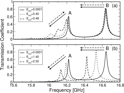
First, we employ the TMM and study the steady-state results. In this situation it is convenient to fix the transmitted (output) field and calculate backwards to find the incident and reflected fields. In Fig. 3 we present a spectral interval including the first two peaks (peaks A, B) above the band gap of Stack 2 for several fixed transmitted field strengths and different directions of incidence. The inclusion of the defect shifts all peaks in Fig. 2(b) to slightly lower frequency in the linear regime. Due to the nonlinear properties of the defect, the frequencies of the transmission resonances vary with the local electric field intensity which in turn varies with the output field. Since the behavior of peak B is very similar for the two directions of incidence, the output field strengths in the figure are chosen to highlight the behavior of peak A. The frequency shift of peak A occurs at very different output field strengths depending on the direction of incidence. As the input field is increased, all the transmission peaks shift to lower frequencies (solid arrows in Fig. 3). The curves are presented with fixed output field and one notices that all peaks shift to lower frequencies with increased output field (dashed arrows in Fig. 3), except for peak A in the case of incidence from the left [Fig. 3(a)], which moves to higher frequencies. This opposite shift in frequency means that while generally the output field at the transmission peak increases with increased input field, for this peak the output field actually decreases as the input field is increased. Referring to Fig. 2(b) one notices that peak A is located slightly above a band gap of the central stack (Stack 2). With increased input intensity the nonlinear defect shifts the peak to lower frequency such that it moves deeper into the band gap and becomes increasingly suppressed. Behavior similar to peak A is also found for the first peak (peak C) above the first Bragg band gap of Stack 2 (not shown).
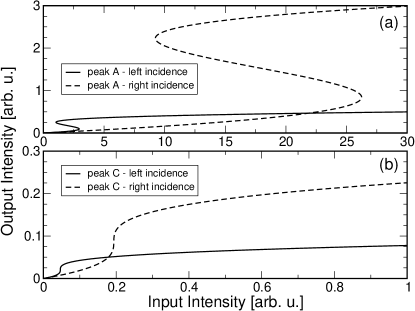
Next, in Fig. 4, we compare the output intensity as a function of input intensity for incidence from the two opposite sides at frequencies with equal relative detuning from peak A and peak C, calculated using the TMM. We find strong nonreciprocity in all cases. The transmission in the two directions differs by up to a factor of 6 for peak A and a factor of 4 for peak C. Peak A also shows strong bistability for both directions. The switching intensity threshold for incidence from the left is almost an order of magnitude lower than for incidence from the right. With the given detuning from the linear transmission peak frequency one finds no bistability for peak C but with stronger detuning bistability does appear. Such bistability in an optical diode was previously mentioned in Tocci et al. (1995); Chen et al. (2003).
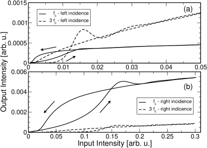
Finally, we simulate the transmission using the PSTD method. This time-domain method inherently includes the higher harmonics that may occur due to the nonlinear material. We use a spatial step-size of and a temporal step-size of . The incident field was chosen as a long Gaussian pulse with peak amplitude , carrier frequency GHz (peak A) and width parameter , to operate in a regime where the envelope magnitude varies slowly. Figure 5 shows the magnitude of the short-time Fourier-transform at the carrier frequency and at its third harmonic. Again, we find that the transmission strongly differs for incidence from the two sides. Transmission at is initially higher for incidence from the left but when the incident intensity reaches 0.04 transmission for incidence from the right becomes greater. On the other hand, the transmission at is always much greater for the pulse incident from the left. At the structure is essentially transparent, as the LH-material slabs have at that frequency. We find bistability for the carrier frequency, as well as, its third harmonic with incidence from either direction. The threshold switching intensities differ greatly for the two directions. The switching intensities for the two frequencies with a particular direction of incidence are very similar to one another. These results agree well with the TMM calculation.
In our PSTD simulations we also encountered modulational-instability-like behavior in this system with different threshold intensities for the onset of this instability. This effect will be subject to further investigation.
In conclusion, we have studied numerically the linear and nonlinear transmission of a novel type of multilayer structures composed of two different dielectric materials. We have shown that asymmetric periodic structures with nonlinear layers can demonstrate highly nonreciprocal transmission which is a major characteristic of an optical diode. We have analyzed the properties of the left-handed diode by employing the transfer-matrix approach and direct pseudospectral time-domain numerical simulations, and have shown its bistable behavior.
References
- Scalora et al. (1994) M. Scalora, J. P. Dowling, C. M. Bowden, and M. J. Bloemer, J. Appl. Phys. 76, 2023 (1994).
- Tocci et al. (1995) M. D. Tocci, M. J. Bloemer, M. Scalora, J. P. Dowling, and C. M. Bowden, Appl. Phys. Lett. 66, 2324 (1995).
- Liang et al. (1997) J. J. Liang, S. T. Lau, M. H. Leary, and J. M. Ballantyne, Appl. Phys. Lett. 70, 1192 (1997).
- Gallo and Assanto (1999) K. Gallo and G. Assanto, J. Opt. Soc. Am. B 16, 267 (1999).
- Mujumdar and Ramachandran (2001) S. Mujumdar and H. Ramachandran, Opt. Lett. 26, 929 (2001).
- Gawith et al. (2001) C. B. E. Gawith, P. Hua, P. G. R. Smith, and G. Cook, Appl. Phys. Lett. 78, 4106 (2001).
- Gallo et al. (2001) K. Gallo, G. Assanto, K. R. Parameswaran, and M. M. Fejer, Appl. Phys. Lett. 79, 314 (2001).
- (8) See Focus issue: Opt. Express 11, 639 (2003).
- Nefedov and Tretyakov (2002) I. S. Nefedov and S. A. Tretyakov, Phys. Rev. E 66, 036611 (2002).
- Li et al. (2003) J. Li, L. Zhou, C. T. Chan, and P. Sheng, Phys. Rev. Lett. 90, 083901 (2003).
- Feise et al. (2004a) M. W. Feise, I. V. Shadrivov, and Yu. S. Kivshar, Appl. Phys. Lett. 85, 1451 (2004a).
- Yeh (1988) P. Yeh, Optical Waves in Layered Media (John Wiley & Sons, New York, 1988).
- Liu (1997) Q. H. Liu, Microw. Opt. Technol. Lett. 15, 158 (1997).
- Lidorikis et al. (1998) E. Lidorikis, K. Busch, Q. M. Li, C. T. Chan, and C. M. Soukoulis, Physica D 113, 346 (1998).
- Berenger (1994) J. P. Berenger, J. Comput. Phys. 114, 185 (1994).
- Feise et al. (2004b) M. W. Feise, J. B. Schneider, and P. J. Bevelacqua, IEEE Trans. Antennas Propag. 52, 2955 (2004b).
- Tran (1996) P. Tran, Opt. Lett. 21, 1138 (1996).
- Chen et al. (2003) L. X. Chen, D. Kim, Y. L. Song, W. Q. Ding, W. H. Lu, and S. T. Liu, Chin. Phys. Lett. 20, 1514 (2003).