CMS Inner Tracker Detector Modules
Abstract
The production of silicon detector modules that will instrument the CMS Inner Tracker has nowadays reached units out of the approximately needed in total, with an overall yield close to . A description of the module design, the assembly procedures and the qualification tests is given. The results of the quality assurance are presented and the experience gained is discussed.
1 Introduction
The CMS Tracker is a cylindrical device of in length and in diameter immersed in a 4 Tesla solenoidal magnetic field. The innermost region () is occupied by a pixel detector, whereas the remaining volume is instrumented by using silicon microstrip modules organized in 10 cylindrical layers and 12 disks as sketched in Fig. 1, corresponding to more than of active surface. A detailed description of the CMS Silicon Strip Tracker (SST) can be found elsewhere TkTDR . The detector modules described in this paper will instrument the region comprised between and in radius and in , i.e. the innermost four cylindrical layers, known as Tracker Inner Barrel (TIB), and the two groups of three disks at between and , the Tracker Inner Disks (TID), each organized in three concentric rings.
Single-sided and double-sided layers can be distinguished in Fig. 1. Single-sided layers are made of “” modules, whose readout strips lay along the direction for the barrel and along the radial direction for the disks, providing a measurement of the coordinate. The innermost TIB/TID layers are instead double-sided, i.e. equipped with “double-sided” sandwiches capable of a space point measurement and obtained by coupling back-to-back a module and a special “stereo” module with the strips tilted by . The TIB requires 2724 modules, 1536 of which assembled into 768 double-sided sandwiches; the TID requires 816 modules, 576 of which assembled into 288 double-sided sandwiches. In total 3540 modules must be produced, plus of spares.
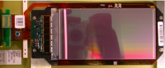
The TIB/TID modules and their components share the same basic structure and design with all other SST modules: as shown in Fig. 2(a), the module consists of a carbon fibre frame that supports the silicon detector and the readout electronics, hosted on a hybrid. The picture of a module is shown in Fig. 2(b).
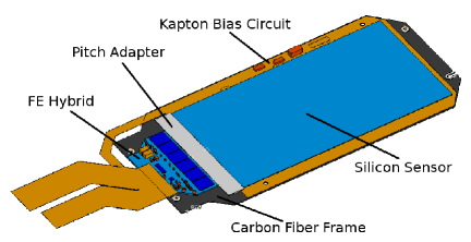
All TIB/TID silicon detectors are radiation hard thick sensors sensors made by Hamamatsu Photonics on 6” wafer lines. Barrel sensors are with 768 strips at in pitch for the two innermost layers, and with 512 strips at in pitch for the outermost layers. Disk detectors have a wedge shaped geometry with several different dimensions and pitches depending on the ring.
The front-end hybrid is made of a kapton circuit (that also integrates the connection tail) laminated onto a ceramic rigidifier. It hosts four or six APV25, the SST front-end chips apv , the additional ASICs (APVMUX, PLL and DCU) and the pitch adapter that allows to match the pitch of the APV25 input pads to the pitch of the sensor readout pads.
2 Module assembly
Building a high precision silicon tracker device requires that the accuracy and the reproducibility of the mechanical assembly of its sub-components lay within few tens of microns, i.e. a figure comparable with the point resolution. This tight requirement is met in our case by means of semi-automatic assembly gantries that have been designed and commissioned for this purpose within the SST community gantry . The “gantry” is a robot based on a micrometric 3D movement that first dispenses the glue on the carbon fibre frame and then places the components (silicon sensors and front-end hybrid) on it. The accuracy is guaranteed by the use of pattern recognition techniques that exploit the presence of fiducial marks on each component. At the end of every operation the gantry itself is able to perform a survey measurement. Typical RMS spread of the relative linear offset between pieces is below , to be compared with acceptance cuts of few tens of microns; the RMS spread of the angular relative offset is , with an acceptance cut of . Out of more than 1500 modules assembled at the gantries, less than are rejected because of assembly precision being out of specifications.
The connections between the silicon strip sensor readout pads and the corresponding pitch adapter lines are made by using wire micro-bonding machines. The bonding of the innermost layer modules with pitch is particularly critical, requiring the bonds to be organized in two overlapping rows between staggered pads. Bias connections for the silicon sensor are also made by three groups of micro-bonds, one on the silicon sensor back and two on the bias ring on the front. Overall, the TIB/TID project requires more that 2M bonds. Such huge numbers require the deployment of state-of-the-art micro-bonding techniques, but this has been certainly achieved since all bonding centers are performing beyond the specifications: the quality control procedure, consisting of pull tests on test bonds (and also on real bonds on a sample basis), have measured an average pull force exceeding , well above the required. More than 0.65M bonds have already been done up to now, with less than of unrepairable failures.
3 Quality control tests
The quality assurance procedure for fully assembled modules consists of two complementary tests. The “module full test” defines the module grading by tagging major functional problems and defective channels; it follows almost immediately the assembly and bonding phases for a fast and effective feedback on possible upstream problems. The “long term test” is performed within a climatic chamber and uses a DAQ system similar to the final one; it is intended to study possible thermally induced mechanical stresses and module infant mortality.
The “module full test” is performed by using a light, compact, standalone and user-friendly test system, known as ARC arc . The test consists of the following measurements: sensor I-V curve up to 450V; pedestal, noise and pulseshape runs; shorted neighbouring channel detection by means of cross-talk; open channel detection by means of LED illumination test, and pinhole detection by means of light-induced sensor leakage current. A “open” is a channel not connected to the corresponding sensor readout strip, whereas “pinhole” is jargon for a short-circuited strip coupling capacitor. Shorts and pinholes cause the lost of the affected channels and, more dangerously, can prevent an entire readout chip from functioning properly. The standard procedure requires these channels to be disconnected from the readout electronic once identified.
The current versus voltage (I-V) measurements on the silicon sensors show a modest degradation with respect to bare sensor measurements. The I-V curves of modules are shown in Fig. 3. The current distribution at 450V shows a bulk around and only 24 out of more than modules () do not comply with the acceptance cut (I(450V)).
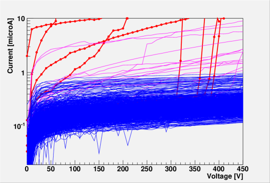
These failures, concentrated in the early production, have been traced back to be mainly due to a defective sensor manipulation tool causing scratches, as later spotted by the detailed optical inspection that all modules also undergo.
A module is also classified as bad if the number of defective channels exceed of the total. A channel or strip is considered bad if flagged as dead, noisy, shorted, open or pinhole. Only of modules have been rejected for this reason up to now: of over k strips only 1k bad channels have been identified (), approximately half as noisy and half as opens (thus including also unbonded pinholes and shorts).
The long term test is performed into a climatic chamber, that hosts up to 10 modules, and by which temperature and humidity are controlled. The test, lasting days, is intended as a real module burn-in, and consists of the continuous readout of the modules during multiple thermal cycles between room temperature and C to emulate the real operating conditions within CMS. Over more than a thousand modules tested, only 11 () have failed the long term test. Among them, only one was lost for a suspected stress-induced failure. The others showed DAQ errors that in all likelihood are not related to the modules themselves. Most significantly no new bad channel has been found after the multiple thermal cycles.
All modules identified as bad, i.e. not complying with the tight quality requirements at any point of the testing procedure, are now being collected in a specialized diagnosis and repair center for further deep investigation and possible recovery.
4 Conclusions
After one year of full activity, the TIB/TID community has reached of the total module production ( out of pieces). The overall yield is stable, around . No major sensor-related failures have been encountered thanks to the excellent sensor quality and their effective screening. The module design has been demonstrated to be robust and the excellent yield proves that the assembly, bonding and testing procedures are safe and reliable.
References
- (1) CMS Collaboration, CERN-LHCC/98-6 (1998); CMS Collaboration, CERN-LHCC/2000-16 (2000).
- (2) J.L. Agram et al., Nucl. Instr. Meth. A 517 (2004) 77.
- (3) L.L. Jones, APV25-S1 User Guide, Version 2.2, Rutherford Appleton Laboratory, Oxfordshire.
- (4) A. Honma, et al., CMS Note 2002/005.
- (5) M. Axer et al., CMS Note 2001/046. (2004) 321.