Full Hydrodynamic Simulation of GaAs MESFET’s
Abstract
A finite difference upwind discretization scheme in two dimensions is presented in detail for the transient simulation of the highly coupled non-linear partial differential equations of the full hydrodynamic model, providing thereby a practical engineering tool for improved charge carrier transport simulations at high electric fields and frequencies. The discretization scheme preserves the conservation and transportive properties of the equations. The hydrodynamic model is able to describe inertia effects which play an increasing role in different fields of micro- and optoelectronics, where simplified charge transport models like the drift-diffusion model and the energy balance model are no longer applicable. Results of extensive numerical simulations are shown for a two-dimensional MESFET device. A comparison of the hydrodynamic model to the commonly used energy balance model is given and the accuracy of the results is discussed.
keywords:
Semiconductor device modeling; charge transport models; hydrodynamic model; upwind discretization; submicron devices; hot electrons; velocity overshoot, Monte Carlo methods, MESFETs.4359172804
A. Aste et al. Full Hydrodynamic Model
Andreas Aste, Institute for Theoretical Physics, Klingelbergstrasse 82, 4054 Basel, Switzerland
1 INTRODUCTION
There is a growing interest in extended charge transport models for semiconductor devices. Our paper emerges from the the fact that today’s submicron semiconductor devices like e.g. MESFETs and HEMTs are operated under strong electric fields and at high frequencies. Information transmission using an electromagnetic wave at very high frequencies will have a direct impact on how we design active and passive components in different fields of micro- and optoelectronics. In such cases, quasi-static semiconductor device models like the energy balance model (EBM) are no longer adequate. Especially in GaAs and related materials used for high-speed device design, inertia effects play an important role since the momentum and energy relaxation times of the electron gas are close to the picosecond range.
The most elaborate and practicable approach for the description of charge transport in semiconductors used for device simulation would be the Monte Carlo (MC) method . The advantage of this technique is a complete picture of carrier dynamics with reference to microscopic material parameters, e.g. effective masses and scattering parameters. But the method must be still considered as very time consuming and hence too uneconomical to be used by device designers.
Besides the simplest concept which is the traditional drift-diffusion model (DDM), there is a much more rigorous approach to the problem, namely the so-called hydrodynamic model (HDM). A simplified version of the HDM is the EBM, which is implemented in most of today’s commercial semiconductor device simulators. The HDM makes use of electron temperature for the description of charge transport and takes inertia effects into account as well. Starting from the Boltzmann equation, Blotekjaer [2] and many others presented a derivation of such equations under the assumption of parabolic band structures. Especially for silicon, satisfactory results were obtained this way [3]. But the results have often been unsatisfactory when MC models based on a nonparabolic structure were compared to HDM results based on an empirical choice of model parameters. Therefore, it is quite natural to improve the HDM by incorporating energy-dependent relaxation times and effective masses obtained from MC bulk simulations [4, 5]. This is a strategy we pursue in this paper.
In the first part of this work, we give a short definition of the hydrodynamic model for GaAs. We emphasize that a thorough analysis of the physical features of the charge carrier transport models is the basis for a clear understanding of their limits of applicability. Then we give a simple discretization scheme for the full hydrodynamic model in two dimensions, which will be applied to a GaAs MESFET structure in the last part. There, we compare the HDM results also to results obtained from the simpler EBM, and we investigate the influence of the grid resolution on the results.
2 THE HYDRODYNAMIC MODEL FOR GaAs FETs
2.1 Definition of the model
Our active device model is based on the single-gas hydrodynamic equations. This is a simplification of the two-valley hydrodynamic equations, since strictly speaking, in GaAs and other semiconductors with similar band structure like InP, there exists an electron gas with different thermal distribution function for each conduction band valley (i.e. the - and -valleys). The equations for each valley are, however, coupled through collision terms since electrons can scatter between two different valleys. The corresponding relaxation rates may be of the order of a picosecond and are therefore relatively large. This is the main drawback of the single-gas approximation, and it would be desirable to implement at least a two-valley hydrodynamic model. Reliable extensive two-valley simulations have been performed only for the one-dimensional case so far due to the large amount of equations and parameters involved in such a model. A hydrodynamic two-valley simulation of GaAs MESFETs is the subject of one of our forthcoming papers. The HDM equations consist of the continuity equation
| (1) |
for negligible charge carrier generation and recombination, the momentum balance equation given by
| (2) |
or alternatively (only for the x-component)
| (3) |
and the energy balance equation
| (4) |
where , (), and are the electron density, the electron energy density (average electron energy) and the electron drift velocity, respectively. is the x-component of the electron drift velocity and the momentum density. Corresponding equations are valid for the y- (and z-) components. is the electron temperature, the elemental charge and Boltzmann’s constant. is the average thermal equilibrium energy of electrons, where is the lattice temperature. The EBM uses only a simplified energy balance equation (see below). The electronic current density inside the active device is given by
| (5) |
the total current density is
| (6) |
The momentum relaxation time is related to the mobility of the electrons via , and the energy relaxation time describes the exchange of energy between the heated electron gas and the lattice. and and the effective electron mass are assumed to be functions of the mean electron energy. We performed steady-state Monte Carlo simulations in order to get the correct values for these parameters.
The hydrodynamic equations, together with Poisson’s equation ( is the number of (ionized) donors)
| (7) |
form a complete set of equations that can be used to solve for the electron density, velocity, energy and electric field for given boundary conditions, if we use a closing relation for the mean electron energy , the electron temperature and velocity :
| (8) |
The reason for the double index of the electron mass will soon become clear. The last term in eq. (8) accounts for the fact that a minimum energy eV is necessary to excite an electron to an upper conduction band. is the relative fraction of electrons in the L-band for the stationary homogeneous case. The term is often neglected in the literature, but this may lead to an overestimation of the electron temperature of more than 1000 K at high energies.
2.2 Remarks on the single gas approximation
We point out again the important fact that we are using a single-gas approximation for the hydrodynamic model. This means that the closing relation eq. (8) is a crude approximation which allows the calculation of the electron temperature from the total electron energy and electron drift velocity. Some authors neglect also the influence of the electron velocity on the temperature [5, 6] by directly relating the electron temperature to the average electron energy from stationary MC simulations.
The transition from the two-gas model to the single-gas approximation has to be done carefully; therefore, we present here a short discussion of the problem which is usually not mentioned in the literature. We assume parabolic and valleys for the sake of brevity, but in our simulations, we took the effect of the non-parabolicity of the energy bands into account by using the Kane model [7], which generalizes the parabolic relation for the electron energy and electron crystal momentum
| (9) |
to
| (10) |
with the non-parabolicity coefficient which has different values for the different energy bands. is the effective electron mass at the bottom of the energy band under consideration. Very often, an energy-dependent electron mass is defined via
| (11) | |||||
| (12) |
i.e. the electron mass increases with growing energy. The electron mass must not be confused with the energy-dependent electron mass used in the hydrodynamic model. In that case, the masses are a kind of average masses depending on the average electron energy.
There is even a further aspect related to the notion of the electron mass. The crystal velocity of an electron is given for spherical bands by
| (13) |
A short calculation for the Kane model shows that
| (14) |
which implies that crystal velocity and crystal momentum are related by
| (15) |
i.e. a different definition of the energy-dependent electron mass applies if the electron velocity is calculated from the crystal momentum.
In the single particle two-band MC simulations, the random walk of an electron inside the semiconductor material is monitored over a sufficiently long time. As a result, the probability that an electron resides in the valley is obtained as a function of the applied constant homogeneous electric field or as a function of the mean electron energy , and the probability of finding the electron in an upper valley is then . Also the values for for the average electron velocities and in the different valleys are obtained as well. Then it is reasonable to define the average electron velocity by
| (16) |
The average electron momentum is given by
| (17) |
hence the (energy-dependent) electron mass which must be used in the hydrodynamic model in order to relate average electron velocity and electron momentum is calculated from
| (18) |
But we suggest that a different mass should be used for the calculation of the average kinetic electron energy in eq. (8). We identify
| (19) |
and therefore
| (20) |
and are not distinguished in the literature. It is tempting to use a naive definition for the electron mass
| (21) |
It is interesting that data in the literature for the energy-dependent electron mass are usually in better agreement with this definition. It is clear that the HDM is still an approximative description of charge carrier dynamics inside a semiconductor, and the different assumptions which are inherent in the derivation of the model may already cause larger errors in the simulation results than using only one mass. Therefore we do not claim that our discussion leads to improved simulation results, but it rather shows the limits of the frequently used model and points out that it is mandatory to maintain always a highest possible degree of consistency.
Figure 1 shows , and normalized to the free electron mass as functions of the average electron energy for a GaAs lattice temperature K and a low doping density . The results from MC simulations were smoothed by a polynomial fit and transferred afterwards into the hydrodynamic simulation program. We used and . For high energies when nearly all electrons are in the upper bands, the electron mass even exceeds the value due to the non-parabolicity of the energy bands.
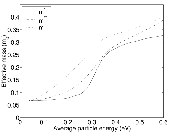
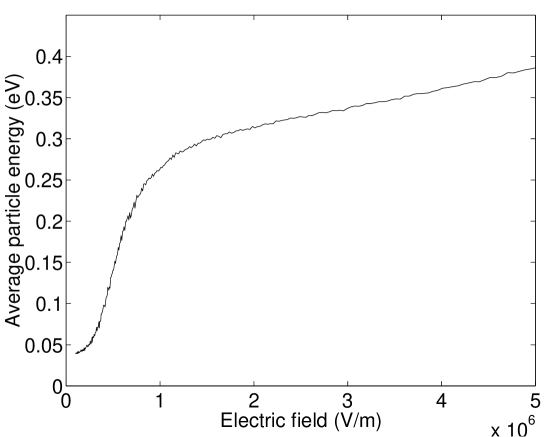
Figure 2 shows the average energy of an electron in a constant homogeneous electric field E for GaAs. For each data point, the electron was scattered one million times (including so-called self-scattering), therefore the resulting curve is already quite smooth. It is clear that MC simulations deliver no data for average electron energies below meV, since the mean electron energy has this value if no electric field is applied to the crystal, and grows for increasing electric field. This is no major problem, since the low energy region is of minor importance for the hydrodynamic simulation and the necessary data can be obtained from theoretical considerations [4].
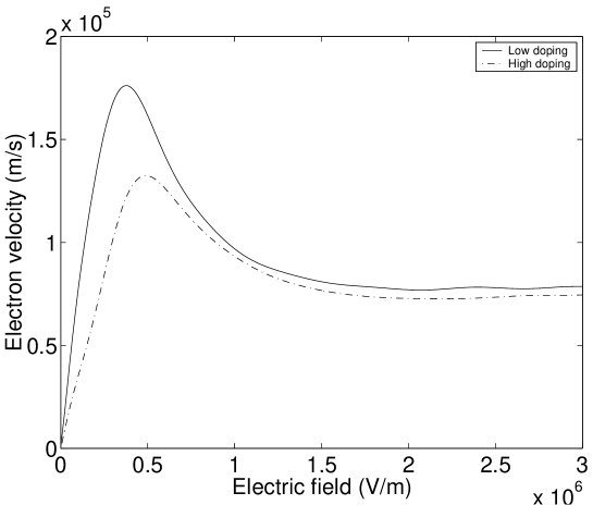
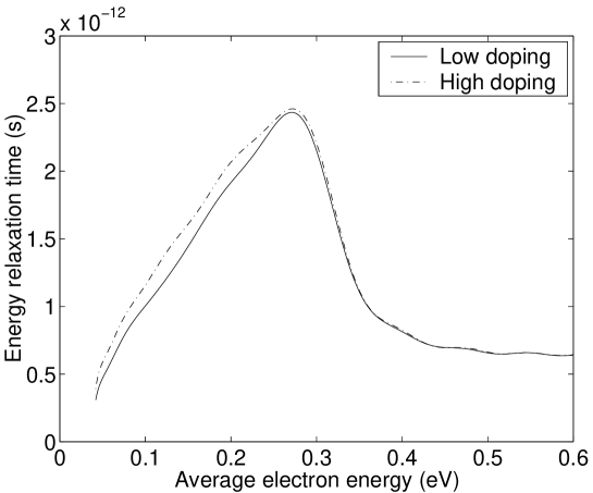
In order to complete the set of data which is necessary for hydrodynamic simulations, the electron velocity and energy relaxation times are depicted in Figs. 3 and 4 for doping densities and . The characteristic shape of the velocity curve can be explained by the fact that at high energies the electrons jump into the bands where the electrons have a lower mobility than in the band.
Finally, we need an expression for the thermal conductivity of the electron gas, which is given by theoretical considerations
| (22) |
Several different choices for can be found in the literature, and many authors [4, 5] even neglect heat conduction in their models. As a matter of fact, heat conduction does not influence the simulation results very much if remains within a reasonable range, but Baccarani and Wordeman point out in [8] that neglecting thermal conductivity completely can lead to nonphysical results and mathematical instability. Although their work is directed to Si, their remarks should be equally valid for GaAs since the equations have a similar form in both cases. In our simulations, we have chosen .
2.3 The energy balance model
The EBM is obtained as a simplification of the full HDM by neglecting the convective terms of the momentum balance equation (3). Additionally, the energy balance equation (4) is simplified by the assumption that the time derivative of the mean electron energy is small compared to the other terms and that the kinetic part in can also be neglected, i.e.
| (23) |
or, if we take the two-valley structure of GaAs into account,
| (24) |
The energy balance equation then becomes
| (25) |
and the momentum balance equation simplifies to the well-known current equation
| (26) |
The continuity equation and the Poisson equation remain of course unchanged in the EBM. Neglecting the time derivative of the current density is equivalent to the assumption that the electron momentum is able to adjust itself to a change in the electric field within a very short time. While this assumption is justified for relatively long-gated field effect transistors, it needs to be investigated for short-gate cases.
Setting the electron temperature equal to the (constant) temperature of the semiconductor material leads to the drift-diffusion model. Such a simplification is clearly not justified for the case studied in this paper (see also [9]).
3 NUMERICAL ASPECTS
3.1 Discretization of the equations
Today, many elaborate discretization methods are available for the DDM equations or EBM equations. The well-known Scharfetter-Gummel method [10] for the DDM makes use of the fact that the current density is a slowly varying quantity. The current equation is then solved exactly under the assumption of a constant current density over a discretization cell, which leads to an improved expression for the current density than it is given by simple central differences. It is therefore possible to implement physical arguments into the discretization method. Similar techniques have been worked out for the EBM [11]. But due to the complexity of the HDM equations, no satisfactory discretization methods which include physical input are available for this case.
Therefore, we developed a shock-capturing upwind discretization method, which has the advantage of being simple and reliable. For our purposes, it was sufficient to use a homogeneous mesh and a constant time step. But the method can be generalized to the non-homogeneous case.
Time discretization is done for all equations by forward Euler differencing, i.e. the discretization scheme is fully explicit. The discretization is always written down only for the x-component of vectorial quantities in the sequel, since the corresponding expressions for y-components are then easy to derive.
The constant timestep used in our simulations was typically of the order of a few tenths of a femtosecond, and quantities at time carry an upper integer index .
The rectangular simulated region of the MESFET gets discretized into rectangular cells of equal size . Scalar quantities at timestep like and , where and are located at the center of the cells, whereas vectorial quantities like e.g. the electric field components , or the velocity components , are always calculated first at midpoints between the scalar quantities.
If necessary, we can define intermediate values, e.g. by
| (27) |
but a different definition applies to e.g. , as we shall see.
The fundamental variables that we will have to compute at each timestep are , , (or ), and , always respecting the imposed boundary conditions. All other variables used in the sequel should be considered as derived quantities.
The momentum balance equation is discretized in the following way:
| (28) | |||
| (29) | |||
| (30) |
where and and the same discretization strategy is applied to the y-component of the electron velocity. From the momentum density we obtain the new particle current density by
| (31) |
and the momentum density at is extrapolated from neighbouring points in the direction of the electron flow x-component
| (32) |
and finally we get
| (33) |
| (34) |
We found that the purely heuristic choice
| (35) |
in the equations above improves the stability of our code.
The electron temperature is related to the energy density by the relation and can therefore be regarded as a dependent variable. The upwind discretization is of the energy balance equation is given by
| (36) | |||||
where we have defined the energy currents
| (37) |
| (38) |
and
| (39) |
Having obtained the new values for the mean electron energy, the transport parameters and energy-dependent masses are then also updated.
The current continuity equation is discretized in a conservative way, using the particle current density
| (40) |
i.e. particles that leave cell in x-direction enter cell and analogously for the y-direction; therefore, the total number of electrons inside the MESFET can only be changed at the boundary of the simulation region (mainly at the contacts).
The Poisson equation, which is coupled to the hydrodynamic equations only through the particle density , can be solved by any convenient method which is fast enough, since the computational effort should be kept as small as possible. Therefore, we used a multigrid method to perform this task. Fortunately, the Poisson equation has not to be solved at each timestep. Since the relaxation times of GaAs are of the order of some tenths of a picosecond, a timestep of about ten femtoseconds is fully sufficient for the update of the electric field. Fortunately, the stability of the discretization scheme is not affected that way, and allows an enormous reduction of the computational costs.
3.2 Boundary conditions
For the basic quantities and we imposed Dirichlet boundary conditions at each timestep at the contacts, e.g. the potential at the source and the drain was fixed by the applied voltage
| (41) |
Analogously, we assumed charge neutral contacts at the source and the drain, such that the charge carrier density was given there by the fixed doping density. The gate contact was modelled by assuming a Schottky barrier height of 0.8 V. For further details concerning the metal-semiconductor contact modelling we refer to standard textbooks . As far as the energy density is concerned, we imposed the boundary conditions directly on the electron temperature by assuming that the electron gas is in thermal equilibrium with the drain/source contacts.
The artificial boundaries were modelled using von Neumann type boundary conditions. We present an explicit example in order to illustrate this point. We assume that the discrete values of the electron density at the MESFET boundary between the source and the gate (see Fig. 5) are given by : The first index denotes the horizontal direction, whereas the second index starts with at the top of the MESFET. Then, after each update of the density according to eq. (40), we enforce
| (42) |
corresponding to the von Neumann condition that the normal component of the electron density vanishes at the specified boundaries.
As mentioned above, we used a multigrid algorithm to calculate the electric potential. Also there, the mixed Dirichlet/von Neumann boundary conditions were imposed on the subgrids at each intermediate step of the calculations. A FORTRAN90 program which calculates the potential by a multigrid algorithm can be obtained from the first author’s address.
4 SIMULATION RESULTS
The GaAs MESFET structure used in our simulation is shown in Fig. 5. The structure consists of a 0.1 m-thick active layer with a doping concentration of on a 0.3 m buffer layer (). The doping profile is abrupt between the two layers, the lattice temperature is K. For steady-state results, we used long simulation times of 30 ps such that the steady state was de facto reached. The length of the drain and source contacts is 0.5 m, the gate-source separation 0.5 m, the gate-drain separation is 1.0 m and the gate length is 0.8 m. The Schottky barrier height is assumed to be 0.8 V.

In order to obtain stable and physically meaningful results, values like nm for a grid size of were typical values used in the simulations. The rather large mesh was manageable due to the effective multigrid algorithm used for the solution of the Poisson equation. We found that the mesh size used in [5] was too coarse for accurate results, although the authors improve accuracy and convergence speed of their calculations by using a non-homogeneous grid. In fact, a non-homogeneous grid necessitates additional calculational costs which reduce the speed of the simulation, and the timesteps also depend on the size of the smallest cells. Furthermore, the Poisson equation was solved by a conventional successive overrelaxation method.
We present results for a gate-source bias V and a drain-source bias V.
Fig. 6 shows the electron temperature inside the MESFET for the stationary case.
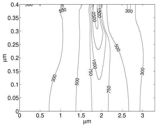
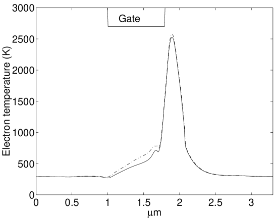
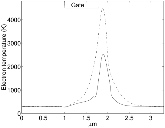
Fig. 7 and 8 show the electron velocity and the electron temperature along the channel of the MESFET (0.077 m below the contacts). Due to the high temperature which is reached under the gate, the electron mobility is strongly lowered in this region. The electrons, which overshoot under the gate, are therefore deaccelerated abruptly to a lower velocity in the high-temperature region. The results obtained from an energy balance calculation are in good quantitative agreement, the differences are mostly pronounced in the region where the electron velocity is high, as it is expected from the different treatment of the energy density in the HDM and EBM.
In the very close vicinity of the gate, it was necessary to reduce artificially the electric field or the velocity of the electrons in order to stabilize our code. We checked that this does not strongly affect the simulations results outside this region due to the very low density of the electron gas near the contact; a similar procedure was also necessary in [5, 6].
The velocity and temperature curves are in fact very similar to those of one-dimensional simulations of ballistic diodes (-structures), which were used as simplified models for FET channels.
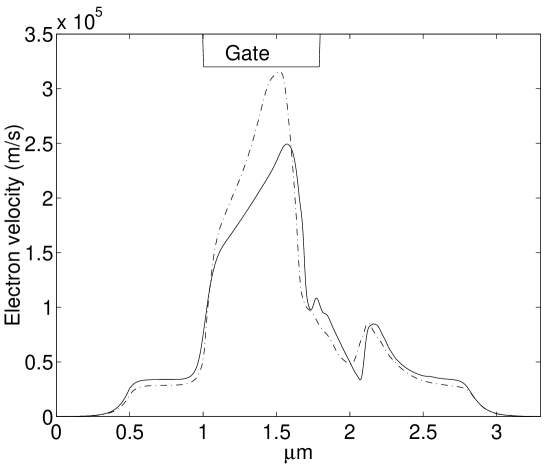
It is interesting to observe in Fig. 7 that our simulation results for a coarse grid (grid size ) are very close to those presented in Fig. 5 in [5], where a non-uniform mesh of typical size was used for a similar MESFET geometry. This may be considered as a confirmation of the results given in [5] for a relatively coars grid, but demonstrates the fact that stability of the code does not automatically imply accuracy of the results, and an investigation of the dependence of the results on the grid resolution is indispensable. The channel below the gate (see also Fig. 10), which is the most interesting region in the MESFET, is relatively small and must be resolved sufficiently.
Due to the strong heating of the electron gas in the channel region, most electrons are excited to the L-band. This leads to a cooling effect of the electron gas, since the excitation energy is missing in the thermal energy balance. The dash-dotted curve in Fig. 9 shows the electron temperature that would be obtained from the HDM if the energy term in eq. (8) were neglected. The energy eV which is necessary to excite an electron to the upper conduction band corresponds to a temperature difference ; the observed error is of the same size.
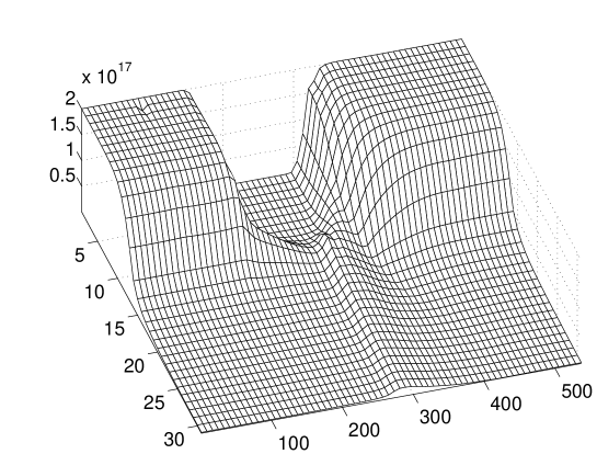
Finally, Fig. 10 shows a surface plot of the electron density inside the device. Clearly visible is the MESFET channel under the gate.
5 CONCLUSION
The feasibility of two-dimensional hydrodynamic simulations is demonstrated for the case of a GaAs MESFET structure. Although the single-gas hydrodynamic model is superior to the drift-diffusion or energy balance model, it is desirable to direct the efforts of future research in the direction of multi-valley hydrodynamic models. Models like the EBM will no longer be adequate for the physical description of high-speed submicron devices in the near future.
It is obvious that future attempts to model submicron devices will face many more problems which have not been touched in this paper. One difficulty is the fact that the components of semiconductor devices are often of very different size and material composition. This necessitates the use of adaptive discretization grids or the hybridization of different numerical methods, but both strategies are hampered by severe problems like numerical instabilities or huge computational efforts for realistic simulations. Another class of problems is due to the fact that the physics of semiconductor materials is very complex, and therefore hard to implement such that the physical behavior of the device is satisfactorily described. Attempts to describe quantum effects in device modelling should be considered as tentative in the case of heterostructure devices. There is no optimal solution for these problems, and the numerical and physical models have to be adapted to the problem under study. We hope that our detailed description of a hydrodynamic simulation may serve also as a help for researchers entering the field of hydrodynamic semiconductor device modelling.
References
- [1] K. Tomizawa, Numerical simulation of submicron semiconductor devices. Artech House: London, Boston, 1993.
- [2] K. Blotekjaer,”Transport equations for electrons in two-valley semiconductors,” IEEE Trans. Electron Dev., vol. 17, no. 1, pp. 38-47, Jan. 1970.
- [3] C.L. Gardner, ”Numerical simulation of a steady-state electron shock wave in a submicrometer semiconductor device,” IEEE Trans. Electron Dev., vol. 38, no. 2, pp. 392-398, Feb. 1991.
- [4] Y.K. Feng, A. Hintz, ”Simulation of submicrometer GaAs MESFETs using a full dynamic transport model,” IEEE Trans. Electron Dev., vol. 35, no. 9, pp. 1419-1431, Sept. 1988.
- [5] M.A. Alsunaidi, S.M. Hammadi, S.M. El-Ghazaly, ”A parallel implementation of a two-dimensional hydrodynamic model for microwave semiconductor device including inertia effects in momentum relaxation,” Int. J. Num. Mod.: Netw. Dev. Fields, vol. 10, no. 2, pp. 107-119, March-April 1997.
- [6] S.M. El-Ghazaly, private communication.
- [7] E.O. Kane, ”Band structure of Indium Antimonide,” J. Phys. Chem. Solids, vol. 1, pp. 249-261, 1957.
- [8] G. Baccarani, M.R. Wordemann, ”An investigation of steady-state velocity overshoot in silicon,” Solid-State Electronics, vol. 28, pp. 407-416, 1985.
- [9] A. Aste, R. Vahldieck, ”Time-domain simulation of the full hydrodynamic model”,Int. J. Num. Mod.: Netw. Dev. Fields, vol. 16, no.2, pp. 161-174, 2003.
- [10] D.L. Scharfetter, H.K. Gummel, ”Large-signal analysis of a silicon Read diode oscillator,” IEEE Trans. Electron Dev., vol. 16, no.1, pp. 64-77, Jan. 1969.
- [11] T. Tang, ”Extension of the Scharfetter-Gummel algorithm to the energy balance equation,” IEEE Trans. Electron Dev. 1984, vol. 31, no. 12, pp. 1912-1914, Dec. 1984.
Biographies
Andreas Aste received the diploma degree in theoretical physics from the University of Basel, Basel, Switzerland, in 1993, and the Ph.D. degree from the University of Zürich, Zürich, Switzerland, in 1997. From 1997 to 1998 he was a post doctoral assistant at the Institute for Theoretical Physics in Zürich. From 1998 to 2001 he was a research assistant and Project Leader in the Laboratory for Electromagnetic Fields and Microwave Electronics of the Swiss Federal Institute of Technology ETH. Since 2001, he is working as a researcher at the Institute for Theoretical Physics at the University of Basel. Dr. Aste is a member of the American Physical Society APS.
Rüdiger Vahldieck received the Dipl.-Ing. and Dr.-Ing. degrees in electrical engineering from the University of Bremen, Germany, in 1980 and 1983, respectively. From 1984 to 1986, he was a Research Associate at the University of Ottawa, Ottawa, Canada. In 1986, he joined the Department of Electrical and Computer Engineering, University of Victoria, British Columbia, Canada, where he became a Full Professor in 1991. During Fall and Spring 1992-1993, he was visiting scientist at the Ferdinand-Braun-Institute für Hochfrequenztechnik in Berlin, Germany. Since 1997, he is Professor of field theory at the Swiss Federal Institute of Technology, Zürich, Switzerland. His research interests include numerical methods to model electromagnetic fields in the general area of electromagnetic compatibility (EMC) and in particular for computer-aided design of microwave, millimeter wave and opto-electronic integrated circuits.
Prof. Vahldieck, together with three co-authors, received the 1983 Outstanding Publication Award presented by the Institution of Electronic and Radio Engineers. In 1996, he received the 1995 J. K. Mitra Award of the Institution of Electronics and Telecommunication Engineers (IETE) for the best research paper. Since 1981 he has published more than 230 technical papers in books, journals and conferences, mainly in the field of microwave CAD. He is the Past-President of the IEEE 2000 International Zurich Seminar on Broadband Communications (IZS’2000) and since 2003 President and General Chairman of the international Zurich Symposium on Electromagnetic Compatibility. He is a member of the editorial board of the IEEE Transaction on Microwave Theory and Techniques. From 2000 until 2003 he served as an Associate Editor for the IEEE Microwave and Wireless Components Letters and from January 2004 on as the Editor-in-Chief. Since 1992 he serves on the Technical Program Committee of the IEEE International Microwave Symposium, the MTT-S Technical Committee on Microwave Field Theory, and in 1999 on the TPC of the European Microwave Conference. From 1998 until 2003 Professor Vahldieck was the chapter chairman of the IEEE Swiss Joint Chapter on MTT, AP and EMC.
Marcel Rohner received the Dipl.-Ing. and Dr.-Ing. degrees in electrical engineering from the Swiss Federal Institute of Technology, Switzerland, in 1993 and 2002, respectively. Since 1993 he was a research assistant in the Electronics Laboratory of the Swiss Federal Institute of Technology ETH, where he has been working in the area of semiconductor device modeling, Monte-Carlo device simulations, electro-optical sampling, digital filtering, and switched-current circuits. In 2002, he joined the corporate technology center of Leica Geosystems AG in the field of electronic distance measurements.