Fabrication-tolerant high quality factor photonic crystal microcavities
Abstract
A two-dimensional photonic crystal microcavity design supporting a wavelength-scale volume resonant mode with a calculated quality factor () insensitive to deviations in the cavity geometry at the level of is presented. The robustness of the cavity design is confirmed by optical fiber-based measurements of passive cavities fabricated in silicon. For microcavities operating in the nm wavelength band, quality factors between - are measured for significant variations in cavity geometry and for resonant mode normalized frequencies shifted by as much as of the nominal value.
pacs:
42.70.Qs, 42.55.Sa, 42.60.Da, 42.55.PxTwo-dimensional photonic crystal (PC) slab waveguide microcavitiesPainter et al. (1999); Yoshie et al. (2001) offer the promise of simultaneously exhibiting a high quality factor () and an ultra-small, wavelength-scale modal volume (). These two parameters, which physically represent long photon lifetimes and large per photon electric field strengths, respectively, are key to microcavity-enhanced processes in nonlinear optics, quantum optics, and laser physicsChang and Campillo (1996); Kimble (1998); Michler et al. (2000); Santori et al. (2001). Recent progress on PC microcavities has included theoretical work on the design of PC microcavities with predicted factors from to Vučković et al. (2002); Srinivasan and Painter (2002); Ryu et al. (2003), and experimental work demonstrating factors in excess of in InP-based lasersSrinivasan et al. (2003a) and silicon membranesAkahane et al. (2003); Srinivasan et al. (2003b). A range of microcavity designs have been employed in these studies, and in many cases, the experimental achievement of high- is predicated on the ability to fabricate the design with a small margin for error. For example, in Ref. Yoshie et al. (2001), the discrepancy between the fabricated device and the intended design led to a theoretical degradation of from to , consistent with the measured of . Extraordinary control over fabricated geometries has been demonstrated in recent workAkahane et al. (2003), where a shift of nm in the positions of holes surrounding the cavity defect region reduced s as high as by over an order of magnitude. Here, we discuss work on a PC microcavitySrinivasan et al. (2003a, b) that exhibits a degree of robustness, both theoretically and experimentally, to deviations from the nominal design sufficient for s above to be maintained. This robustness in to changes in the PC cavity geometry is of practical importance for future experiments in the aforementioned disciplines, to provide insensitivity to fabrication imperfections, as well as to maintain the flexibility in cavity design required to form resonant modes with a prescribed field pattern and polarization.
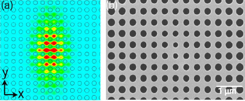
Radiative losses in planar waveguide two-dimensional PC defect microcavities can be separated into in-plane and out-of-plane components, quantified by the quality factors and , respectively, with the total radiative given by . is determined by the size and angular extent (in-plane) of the photonic bandgap, while is determined by the presence of in-plane momentum components () within the waveguide cladding light cone, which are not confined by total internal reflection at the core-cladding interface. In Ref. Srinivasan and Painter (2002), PC microcavities were designed using two mechanisms to avoid radiative loss: (i) use of a mode that is odd about mirror planes normal to its dominant Fourier components, in order to eliminate the DC () part of the in-plane spatial frequency spectrum and hence reduce vertical radiation loss, and (ii) use of a grade in the hole radius to further confine the mode and reduce in-plane radiative losses. The resulting PC microcavity design within the square lattice creates a TE-like (magnetic field predominatly along ) donor-type defect mode (labeled 111This label refers to the mode’s symmetry classification and to it being the lowest frequency mode in the bandgap.) as shown in Fig. 1(a). FDTD simulations of this resonant mode predict a -factor of and an effective modal volume of . We now show how use of mechanisms (i) and (ii) above create a level of robustness in the cavity design.
Use of an odd symmetry mode to suppress vertical radiation loss is, at a basic level, independent of changes in the size of the holes defining the defect cavity. This feature has been confirmed in simulations of simple defect cavity designs in square lattice photonic crystalsSrinivasan and Painter (2002), where did not degrade below , despite significant changes (as much as 40) in the size of the (two) central defect holes. Perturbations that cause the cavity to be asymmetric create a mode which, though not strictly odd, will be a perturbation to an odd mode, and hence will still largely suppress DC Fourier components and exhibit high . However, for the square lattice photonic crystal structures considered here, perturbations to the central defect hole geometry can result in a degradation in , due in part to the lack of a complete in-plane bandgap within the square lattice. This lack of a complete bandgap requires the defect geometry to be tailored so as to eliminate the presence of Fourier components in directions where the lattice is no longer reflective.
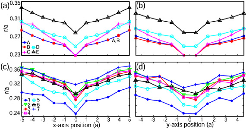
| Cavity | |||||
| PC-A | 0.750 | 0.245 | |||
| PC-B | 0.750 | 0.245 | |||
| PC-C | 0.750 | 0.247 | |||
| PC-D | 0.750 | 0.253 | |||
| PC-E | 0.750 | 0.266 | |||
| PC-1 | 0.879 | 0.241 | - | - | |
| PC-2 | 0.850 | 0.255 | - | - | |
| PC-3 | 0.850 | 0.251 | - | - | |
| PC-4 | 0.842 | 0.251 | - | - | |
| PC-5 | 0.842 | 0.249 | - | - | |
| PC-6 | 0.800 | 0.263 | - | - | |
| PC-7 | 0.800 | 0.270 | - | - |
This tailoring was achieved in Ref. Srinivasan and Painter (2002) by a grade in the hole radius moving from the center of the cavity outwards. The grade, shown in Fig. 1, serves to help eliminate couplings to in-plane radiation modes along the diagonal axes of the square lattice (the -point of the reciprocal lattice) where the PC is no longer highly reflective, while simultaneously providing a means to keep the in-plane reflectivity high along the axis (the direction of the mode’s dominant Fourier components). The use of a large number of holes to define the defect region ensures that no single hole is responsible for creating the potential well that confines the resonant mode, making the design less susceptible to fluctuations in the size of individual holes. Instead, the continuous change in the position of the conduction band-edge resulting from the grade in hole radius creates an approximately harmonic potential wellPainter et al. (2003). This smooth change in the position of the band-edge creates a robust way to mode-match between the central portion of the cavity (where the mode sits) and its exterior. In other workAkahane et al. (2003), softening of this transition is achieved by adjusting the position of two holes surrounding the central cavity region (which consists of three removed air holes in a hexagonal lattice). This method can achieve high-, but as mode-matching is achieved by tailoring only two holes it is more sensitive to perturbations than the adiabatic transition created by a grade in the hole radius. Finally, we note that even though a relatively large number of holes are modified to create the graded lattice, is still wavelength-scale, and remains between - in all of the devices considered in this work. In addition, the methods used here to achieve robustness in are general and can be applied to cavities in other PC latticesSrinivasan and Painter (2003).
To highlight these ideas, 3D FDTD simulations of cavities with varying grades and average normalized hole radius () were performed. Figure 2(a)-(b) shows the grade in along the central and axes for several designs (PC-A through PC-E), and Table 1 lists the calculated resonant frequency, vertical, in-plane, and total factors. In all of these simulations, remains close to , with PC-E showing more significant degradation largely as a result of the increased modal frequency (creating a larger-sized cladding light cone). In addition, an inappropriate choice of grade along the -axis can lead to increased in-plane losses via coupling to -point modes. Nevertheless, the loss in any of the simulated devices did not cause to be reduced below .
To test the sensitivity of the design to perturbations experimentally, cavities were fabricated in a =340 nm thick silicon membrane through a combination of electron beam lithography, inductively-coupled plasma reactive ion etching, and wet etching. Figure 2(c)-(d) shows the values of along the central and axes for a number of fabricated devices (PC-1 through PC-7), as measured with a scanning electron microscope (SEM). Cavities are passively testedSrinivasan et al. (2003b) using an optical fiber taperKnight et al. (1997), which consists of a standard single mode optical fiber that has been heated and stretched to a minimum diameter of 1-2 m. At such sizes, the evanescent field of the fiber mode extends into the surrounding air, providing a means by which the cavity modes can be sourced and out-coupled. The fiber taper is spliced to the output of a fiber-pigtailed scanning tunable laser (1565-1625 nm) with 1 pm resolution, and is mounted (Fig. 3(a)) above and parallel to an array of PC cavities (Fig. 3(b)). When it is brought into close proximity ( nm) to the sample surface, evanescent coupling between the taper and cavity modes occurs.
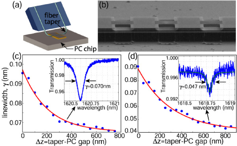
Fig. 3(c)-(d) shows measurements for devices PC-5 and PC-6, which have significantly different profiles (Figure 2(c)-(d)). The inset of Fig. 3(c) shows the normalized taper transmission as a function of wavelength when the taper is nm above cavity PC-5. By measuring the dependence of cavity mode linewidth () on the vertical taper-PC gap () (Fig. 3(c)), an estimate of the true cold-cavity linewidth () is given by the asymptotic value of reached when the taper is far from the cavity. For PC-5, nm, corresponding to . Fig. 3(d) shows the linewidth measurement for PC-6. For this device, nm, corresponding to a . As described in Ref. Srinivasan et al. (2003b), the strength of the taper-PC coupling as a function of taper position can be used to estimate the spatial localization of the cavity field; these measurements closely correspond with calculations and for PC-6 are consistent with an FDTD-predicted . These PC microcavities thus simultaneously exhibit a high- factor that is insensitive to perturbations, and an ultra-small .
Linewidth measurements for each of the cavities PC-1 through PC-7 are compiled in Table 1. The robustness of the to non-idealities in fabrication is clearly evident. Though all of the devices exhibit a general grade in , the steepness of the grade and the average hole radius () vary considerably without reducing below . These high- values are exhibited despite the fact that many cavities are not symmetric (the odd boundary condition is thus only approximately maintained), and the frequency of the cavity resonance varies over a range, between -.
The measured values in Table 1 are still lower than predicted from simulations. This discrepancy is likely due in part to slightly angled etched sidewalls that have been shown in calculations to lead to radiative coupling to TM-like modesTanaka et al. (2003). This non-ideality helps explain why PC-1, which is closest in value to the desired design (PC-A), does not exhibit the highest experimentally. In particular, we have observed that the sidewall angle is poorer for smaller sized holes. On the other end of the spectrum, cavities with the largest hole sizes such as PC-7, which may have more vertical sidewalls, also begin to exhibit higher vertical radiation loss as a result of a larger modal frequency and cladding light cone. In addition, surface roughness is a potential source of loss; for PC-6, which exhibited the highest value, a chemical resist stripping process was used (rather than a plasma de-scum) and may have produced a cleaner, smoother surface.
In summary, the robustness in to errors in the in-plane design of a PC microcavity consisting of a graded square lattice of air holes is discussed. This property is confirmed both by FDTD simulations of devices where the steepness of the grade and the average hole radius are varied without degrading below , and in measurements of microfabricated Si cavities that exhibit factors between - over a wide range of device parameters. For these high- cavities, current limitations on the factor appear to stem principally from slightly angled sidewalls and etched surface roughness, as opposed to errors in the in-plane shape or size of holes.
This work was partly supported by the Charles Lee Powell Foundation. The authors thank M. Borselli for his contributions in building the taper test setup. K.S. thanks the Hertz Foundation for its financial support.
References
- Painter et al. (1999) O. Painter, R. K. Lee, A. Yariv, A. Scherer, J. D. O’Brien, P. D. Dapkus, and I. Kim, Science 284, 1819 (1999).
- Yoshie et al. (2001) T. Yoshie, J. Vučković, A. Scherer, H. Chen, and D. Deppe, Appl. Phys. Lett. 79(26), 4289 (2001).
- Chang and Campillo (1996) R. K. Chang and A. J. Campillo, eds., Optical Processes in Microcavities (World Scientific, Singapore, 1996).
- Kimble (1998) H. J. Kimble, Physica Scripta T76, 127 (1998).
- Michler et al. (2000) P. Michler, A. Kiraz, C. Becher, W. Schoenfeld, P. Petroff, L. Zhang, E. Hu, and A. Imomoglu, Science 290, 2282 (2000).
- Santori et al. (2001) C. Santori, M. Pelton, G. Solomon, Y. Dale, and Y. Yamamoto, Phys. Rev. Lett. 86(8), 1502 (2001).
- Vučković et al. (2002) J. Vučković, M. Lončar, H. Mabuchi, and A. Scherer, Phys. Rev. E 65(1) (2002).
- Srinivasan and Painter (2002) K. Srinivasan and O. Painter, Opt. Express 10(15), 670 (2002).
- Ryu et al. (2003) H.-Y. Ryu, M. Notomi, and Y.-H. Lee, Appl. Phys. Lett. 83(21), 4294 (2003).
- Srinivasan et al. (2003a) K. Srinivasan, P. E. Barclay, O. Painter, J. Chen, A. Y. Cho, and C. Gmachl, Appl. Phys. Lett. 83(10), 1915 (2003a).
- Akahane et al. (2003) Y. Akahane, T. Asano, B.-S. Song, and S. Noda, Nature 425, 944 (2003).
- Srinivasan et al. (2003b) K. Srinivasan, P. E. Barclay, M. Borselli, and O. Painter (2003b), submitted to Phys. Rev. Lett. (available at http://arxiv.org/quant-ph/abs/0309190).
- Painter et al. (2003) O. Painter, K. Srinivasan, and P. Barclay, Phys. Rev. B 68, 035214 (2003).
- Srinivasan and Painter (2003) K. Srinivasan and O. Painter, Opt. Express 11(6), 579 (2003).
- Knight et al. (1997) J. Knight, G. Cheung, F. Jacques, and T. Birks, Opt. Lett. 22(15), 1129 (1997).
- Tanaka et al. (2003) Y. Tanaka, T. Asano, Y. Akahane, B.-S. Song, and S. Noda, Appl. Phys. Lett. 82(11), 1661 (2003).