, , , , ,
Development of a triple GEM UV-photon detector operated in pure CF4 for the PHENIX experiment.
Abstract
Results obtained with a triple GEM detector operated in pure CF4 with and without a reflective CsI photocathode are presented. The detector operates in a stable mode at gains up to 104. A deviation from exponential growth starts to develop when the total charge exceeds e leading to gain saturation when the total charge is e and making the structure relatively robust against discharges. No aging effects are observed in the GEM foils after a total accumulated charge of mC/cm2 at the anode. The ion back-flow current to the reflective photocathode is comparable to the electron current to the anode. However, no significant degradation of the CsI photocathode is observed for a total ion back-flow charge of mC/cm2.
keywords:
GEM , CsI photocathode , UV-photon detector , CF4 , HBDPACS:
29.40.-n , 29.40.Cs , 29.40.Ka , 25.75.-q1 Introduction
A Hadron Blind Detector (HBD) is being considered for an upgrade of the PHENIX detector at the Relativistic Heavy Ion Collider (RHIC) at BNL [1]. The HBD will allow the measurement of electron-positron pairs from the decay of the light vector mesons, , and and the low-mass pair continuum (m 1 GeV/c2) in Au-Au collisions at energies up to 200 GeV. From Monte Carlo simulations and general considerations, the main HBD specifications are: electron identification with very high efficiency (90%), double hit recognition better than 90%, moderate pion rejection factor of about 200, and radiation budget of the order of 1% of a radiation length. The primary choice under study is a windowless Cherenkov detector, operated in pure CF4 in a special proximity focus configuration, with a reflective CsI photocathode and a triple Gas Electron Multiplier (GEM) [2] detector element with a pad readout.
The proposed scheme is significantly different from other HBD designs [3, 4]. The combination of a windowless detector with a CsI photocathode and CF4 results in a very large bandwidth (from 6 to 11.5 eV) and a very high figure of merit N0 = 940. With these unprecedented numbers, one expects approximately 40 detected photo-electrons per incident electron in a 50 cm long radiator, thus ensuring the necessary high levels of single electron detection efficiency and double hit recognition. The scheme foresees the detection of the Cherenkov photoelectrons in a pad plane with the pad size approximately equal to the photoelectron space distribution (10 cm2). This results in a low granularity detector. In addition to that, since the photoelectrons produced by a single electron will be distributed between at most three pads, one can expect a primary charge of at least 10 e per pad allowing to operate the detector at a relatively moderate gain of a few times 103.
In this paper, we report on the operation in pure CF4 of a triple GEM detector, with and without a CsI photocathode evaporated on the top face of the first GEM. Extensive studies using 33 and 1010 cm2 detectors have been performed using a Hg UV lamp, an Fe55 X-ray source and an Am241 alpha source. All measurements were also performed with the conventional Ar/CO2 (70/30%) gas mixture for comparison. Section 2 describes the various setups and conditions under which the measurements were performed. The studies include measurements of the gain amplification curve of the triple GEM structure without (section 3) and with a reflective CsI photocathode (section 5), discharge probability in the presence of the high ionization induced by the Am241 -particles (section 4) and ion back-flow to the photocathode (section 6). A short summary and conclusions are presented at the end of the paper in section 7.
2 Setup and experimental conditions.
For all the measurements, GEMs produced at CERN were used with 50 m kapton thickness, 5 m thick copper layers, 60-80 m diameter holes and 140 m pitch. The GEMs had 33 or 1010 cm2 sensitive areas. These two types of GEMs will be referred to in the text as ”small” and ”large” respectively. Three GEMs were assembled in one stack with G10 frames as shown in Fig. 1. The distance between the GEMs was 1.5 mm and the distance between the bottom GEM (GEM3) and the printed circuit board (PCB) was in most (some) cases 2 mm (1.5 mm). The distance between the top GEM (GEM1) and the drift mesh was 3 mm in the measurements with X-rays and -particles and 1.5 mm in the measurements with UV-photons.
The PCB consisted of 5 strips of 10020 mm2 each. The central group was connected either to a charge sensitive pre-amplifier and shaper or to a picoammeter, depending on the particular measurement. The other groups were grounded.
Two gases were used for the measurements in this work: an Ar/CO2 (70/30%) mixture and CF4. We used a premixed bottle of Ar/CO2 with Ar of 99.999% purity and CO2 of 99.998% purity. The purity of the CF4 was 99.999%.
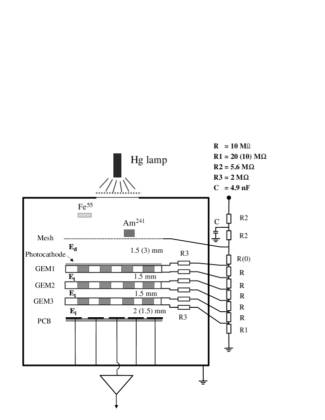
High voltage was supplied to the GEM electrodes via a resistive chain (see Fig. 1). For most of the measurements, the resistors R were equal to 10 M whereas the resistor R1 feeding the gap between GEM3 and PCB (see Fig.1) was equal to 20 M. In some measurements with X-rays and -particles R1 was equal to 10 M. For some measurements an independent voltage supply for selected electrodes was used. In particular, this was required for the measurement of the ion current to the top electrode of GEM1, while studying the ion back-flow (see below).
We use the gap names and the field notations as proposed in [5], i.e. the gap between the mesh and top GEM is called ”drift” and the corresponding field is referred to as Ed; the gaps between GEMs are called ”transfer” and the corresponding fields are referred to as Et; the gap between GEM3 and the PCB is called ”induction” and the corresponding field is referred to as Ei. Most measurements were performed with a 2 mm induction gap and a 20 M resistor feeding it. In this configuration, when the voltage across the GEMs is 510 (370) V, corresponding to a gain of in CF4 (Ar/CO2), the transfer and induction fields are about 3.4 (2.5) kV/cm and 5.1 (3.7) kV/cm, respectively. When R1 is equal to 10 M, the induction fields are half the quoted values. The ability of the GEM to transport electrons through its holes is referred to as ”electron transparency”. It is the product of two factors: the fraction of electrons collected from the top gap into the holes and the fraction of electrons extracted from the holes into the bottom gap. The electron transparency of the GEMs with the voltages and fields indicated above, can be derived from the data presented in [5]. For GEM1 and GEM2 the electron transparency is close to 1, while for GEM3 it is about 0.7 in the case of the lower induction field and approaches 1 for the high induction field.
The photocathode was prepared by evaporating a Å thick layer of CsI on the first GEM previously coated with thin layers of Ni and Au to avoid chemical interaction with the CsI film. For the operation with the reflective photocathode the drift field has to be zero or even reversed in order to collect all the photo-electrons from the CsI layer [6]. For those measurements the corresponding resistor in the chain was shorted. The measurements with the CsI reflective photocathode were performed with a Hg lamp and a UV-transparent window (CaF2) in the cover of the detector box. The lamp was positioned at the detector window with an absorber that reduced the UV flux 1000 times to avoid possible damage of the photocathode [7]. The illuminated area of the detector was about 100 mm2. In this geometry, the measured photo-electron current was about 2106 e/(mms).
The detector assembly (drift mesh, triple-GEM, and PCB) were mounted in a stainless steel box that could be pumped down to torr and was connected to the inlet and outlet gas lines to allow gas flushing. All measurements were done at atmospheric pressure with an overpressure of 0.5 torr in the detector vessel. The system contained also devices for the precise measurement of temperature, pressure and water content down to the ppm level. The Fe55 X-ray source was positioned inside the box at a distance of 40 mm from the mesh. The total rate of X-rays was kept at the level of 1 kHz. 5.9 keV photons from Fe55 release 210 e in Ar/CO2 (26 eV per electron-ion pair) and 110 e in CF4 (54 eV per electron-ion pair) [8].
The discharge limit in the presence of heavily ionizing particles was studied with an Am241 source that emits 5.5 MeV -particles. The source in a container was attached directly to the drift mesh and strongly collimated in order to provide high energy deposition and small energy dispersion in the drift gap. The rate of the -particles varied between Hz. The distance between the active surface of the source and the drift mesh was 10 mm. The range of 5.5 MeV -particles in Ar/CO2 is 39 mm and about 18 mm in CF4. Assuming perpendicular incidence of the -particles to the drift gap, the energy deposition in a 3 mm gas layer is estimated to be 1.1 MeV for CF4 and 0.30 MeV for Ar/CO2 producing 20000 and 12000 primary charges, respectively.
For the study of gain limits we needed a reliable way to monitor the discharges in the triple GEM assembly. The resistor chain voltage was supplied by a HV power supply CAEN N126. This module allowed us to install a protection against over-current with a precision of 0.1 A. The protection threshold was always kept at 5 A above the chain current which was usually in the range between 50 and 100 A. This was enough to cause a trip when a discharge occurred in a single GEM. The trip signal was reset after 1 second and counted by a scaler.
3 Gain in Ar/CO2 and CF4.
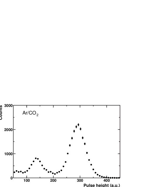
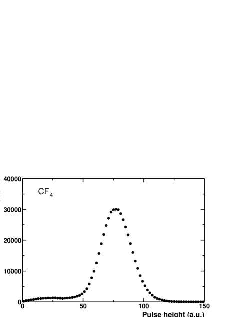
The gain as a function of the voltage across the GEM (VGEM) was measured with all GEMs at the same voltages for both Ar/CO2 and pure CF4. The absolute gas gain was determined from the measurements of the signal from Fe55 5.9 keV X-ray photons. An example of the pulse height spectrum for both gases is shown in Fig. 2. For Ar/CO2 the main peak is very well separated from the escape peak of Ar and the energy resolution is % FWHM. For CF4 the energy resolution is close to 38% FWHM. In both cases the pulse height spectra were measured at a gain higher than .
The gain was calculated, using the measured relationship between the output signal from the amplifier and the input charge to a calibration capacitor and taking into account the average charge produced by one 5.9 keV photon (see previous section).
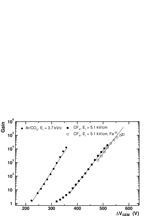
Fig. 3 shows the typical gain curves measured with 5.9 keV X-rays in Ar/CO2 and CF4 using small and large GEMs. Several detector sets were used and good reproducibility between the various sets was observed. Comparing the data for Ar/CO2 and CF4 in Fig. 3 one can see that the operational voltage for CF4 is 140 V higher but the slopes of the gain-voltage characteristics are similar for both gases, i.e. an increase of 20 V in VGEM causes an increase of the gain by a factor of . The gain in CF4 can reach values above , in spite of the very high operational voltage, as was already reported in [11].
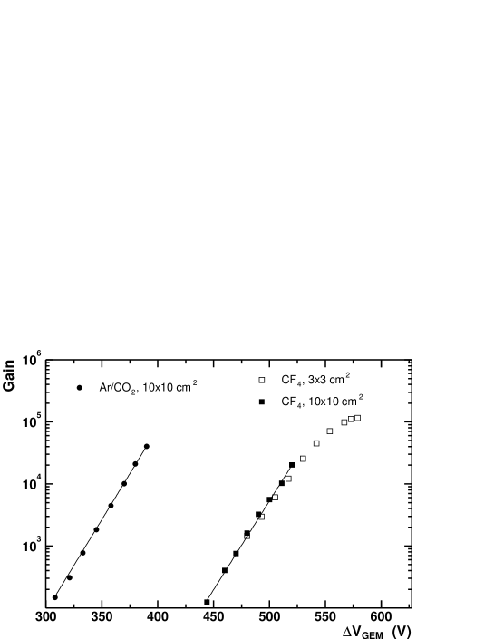
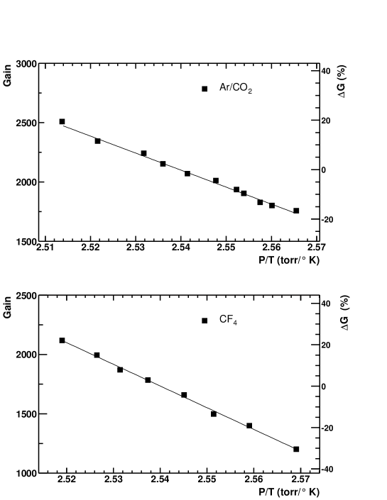
The absolute value of the gain is very sensitive to the gas density. Small variations of the gas pressure () and/or temperature () significantly affect the gain as demonstrated in Fig. 4. A change of 1 in the value causes a gain variation of 17 in Ar/CO2 and of 26 in CF4.
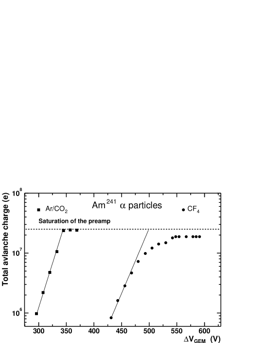
Another feature of CF4 which can be seen in Fig. 3 is the strong deviation from exponential growth at high gains. This “non-linearity” is much more pronounced when the detector is irradiated with Am241 -particles (Fig. 5). In that figure the saturation level of the pre-amplifier is marked with a dashed line. In the case of Ar/CO2 the charge depends on VGEM exponentially, and the signal is saturated by the pre-amplifier. In pure CF4, on the other hand, the dependence of charge versus VGEM becomes non-linear above the value of e and is completely saturated at e, which is below the saturation level of the pre-amplifier. This difference in performance in Ar/CO2 and pure CF4 may be due to the higher primary charge density and lower diffusion in CF4. These two features make the charge cluster in CF4 more compact and dense and, as a consequence, increase the electric field inside the charge cloud resulting in the saturation of the avalanche. This saturation effect is of prime importance for the anticipated application of the HBD in the PHENIX experiment where single photoelectrons are to be detected in a high multiplicity environment of charged particles.
4 Discharge probability in the presence of heavily ionizing particles.
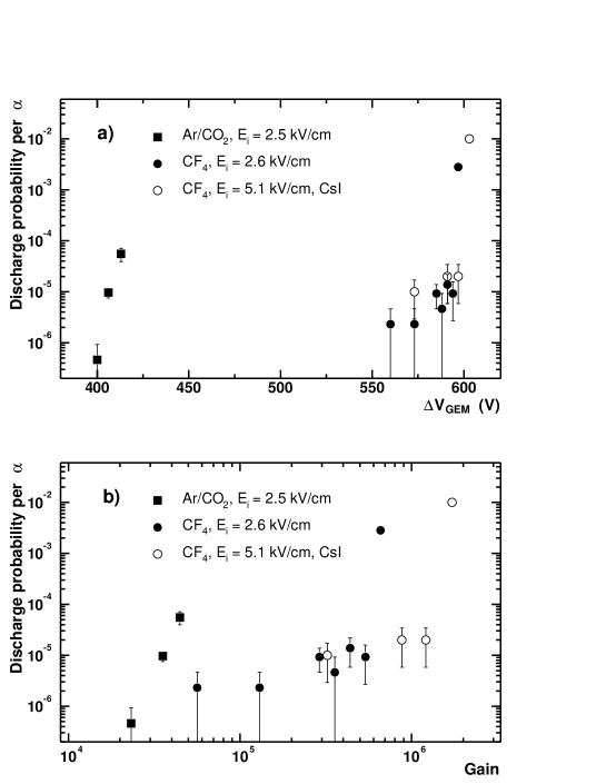
Stability of operation and absence of discharges in the presence of heavily ionizing particles is crucial for the operation of the HBD. The Am241 source was used to simulate heavily ionizing particles under laboratory conditions. We determined quantitatively the probability of discharge as the ratio between the number of discharges within a certain period of time and the number of -particles traversing the detector during the same period. The discharge probability was measured in small GEMs and the results are shown in Figs. 6a and 6b in two different forms: as a function of GEM voltage and as a function of gain.
For the Ar/CO2 mixture the probability of discharge exhibits a rapid increase between 400 V and 420 V across the GEM when the gain reaches . In terms of gain and GEM voltage these results agree with similar data from [9]. In CF4 the discharge probability grows at VGEM above 590 V with both Ei = 2.6 kV/cm and Ei = 5.1 kV/cm. The second setup also had a CsI photocathode on GEM1. From Fig. 5 one can see that the signal from -particles in CF4 is completely saturated above V V at the level of e. As a consequence, the total charge produced by the heavily ionizing particle is limited to below the Raether limit [10] and its ability to provoke a discharge is strongly suppressed. Thus, the gain in CF4 even in the presence of -particles can reach extremely high values of close to . The HBD is expected to operate at gains , i.e. with a comfortable margin below the discharge threshold.
The measurements of the discharge probability were also performed with the large GEM setup. However during the measurement in CF4 the GEMs were severely damaged by the very first spark and a similar study could not be conducted for this setup. The damage to the GEM was severe due to the combination of high operational voltage and high capacitance which results in the energy deposited in the discharge being too high. We plan to repeat the studies with large GEMs with a proper segmentation of the GEMs so as to reduce their capacitance.
5 Operation with the CsI reflective photocathode.
In all the tests with the CsI photocathode a mercury lamp was used for irradiation. In order to determine the total emission from the photocathode itself without any amplification in the GEMs, we applied a positive voltage between GEM1 and the mesh, thus collecting the emitted photo-electrons in the mesh. The operation of the CsI photocathode is shown in Fig. 7, where the photo-electron current as a function of voltage (7a) and time (7b) is plotted. From Fig. 7a it is seen that in order to measure the full photo-electron emission the voltage between the mesh and GEM1 has to exceed 200 V or, since the drift gap was 1.5 mm, the field has to be higher than 1.3 kV/cm, in agreement with [11].
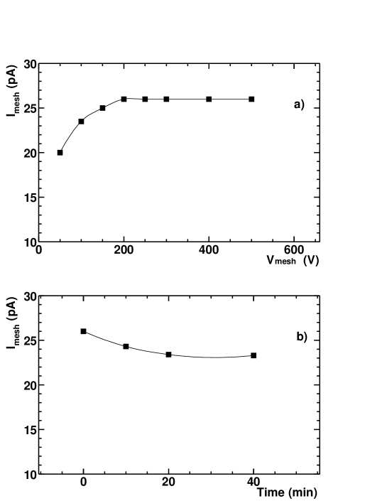
In Fig. 7b the value of the current to the mesh as a function of time is shown, demonstrating that one has to wait about 30 min after the application of the HV in order to stabilize the signal. As CsI is a semi-insulating material, this initial instability of the signal might be caused by polarization and up-charging of the layer.
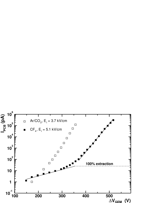
The study of the triple GEM detector with a reflective photocathode was always performed in the regime with Ed = 0. Fig. 8 shows the current to the PCB as a function of the GEM voltage for the small GEM setup. The measurements were done in Ar/CO2 and CF4. In the CF4 curve we can clearly see two regions well described by two exponential dependencies on VGEM (see lines in Fig. 8): an initial slow increase of current at lower voltages related to the increase of the extraction of the photo-electrons from the CsI surface into the holes of GEM1 and a steep exponential increase at higher voltages due to amplification in the GEMs. A detailed discussion of these processes and the transition from one region to the other can be found in [12]. In Ar/CO2 these two regions are not so clearly separated because amplification in this mixture starts at lower voltages. The electron extraction cannot exceed the maximum level shown in Fig. 7a. It indeed seems to reach this level of 100% extraction indicated by the dashed line in Fig. 8. Thus, the gain is determined as the ratio between the current to the PCB and the the extraction current. The latter is given by the first exponential curve up to VGEM = 350 V and by the 100% extraction value at higher values of VGEM.
The gain as a function of VGEM for the setup with the reflective photocathode is shown in Fig. 9. In the same figure the data obtained with X-ray irradiation (Fe55) are also shown in order to demonstrate that the different methods of gain measurement give similar results.
6 Ion back-flow in the triple GEM detector operating with a reflective photocathode.
The flow of positive ions to the CsI layer is one of the potential damaging factors that can cause aging of the photocathode [7, 13, 14, 15]. We call this factor ion back-flow and characterize it by the ratio between the current to the top electrode of GEM1 and the current to the PCB. This ratio depends on both the ion current itself and the fraction of electron current flowing to the PCB. This is a convenient definition as it allows us to estimate the actual ion current from the measured signal at the PCB. In order to measure the current to the photocathode we supplied the voltage separately to the top electrode of GEM1 with a CAEN N126 power supply. The voltages to all other electrodes were supplied through the resistive chain.
In Fig. 10 the ratio of the current to the photocathode and the current to the PCB (ion back-flow factor) as a function of gain is shown for different conditions. The errors on the plots are mainly due to the limited accuracy of the photocathode current measurements. The value of the induction field was changed by changing the corresponding resistor in the chain and the value, indicated in the caption (5.1 kV/cm), is reached at a gain of .
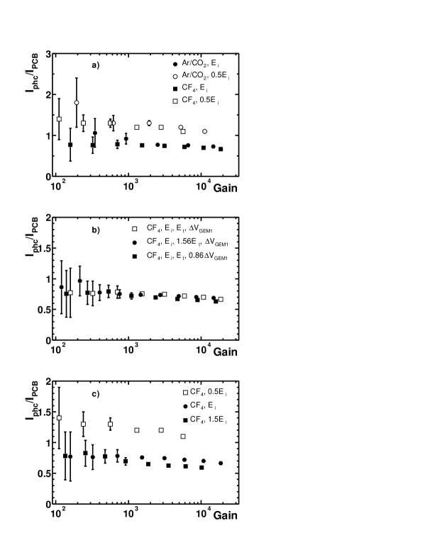
In Fig. 10a we see that in spite of the very different transport properties of the gases used in the measurements no significant dependence of the ion back-flow factor on the nature of the gas is observed as a function of gain and for different induction fields. The insensitivity of the ion back-flow factor to the particular gas at moderate gains is similar to that seen in [14]. It means that the efficiency of the transport of electrons and ions through the GEMs is the same for both gases and does not depend on diffusion.
The insensitivity of the ion back-flow factor to the electric field between the GEMs and in the GEM is demonstrated in Fig. 10b. Here the value of the ion back-flow factor as a function of gain is shown for three different electrostatic conditions: 1) standard, when the transfer field is equal to 3.4 kV/cm for both gaps and the induction field is equal to 5.1 kV/cm (the values refer to a gain of 104), 2) enhanced transfer field in both gaps, 3) reduced field in GEM1. From Fig. 10b we see that neither variation in electrostatic conditions between nor inside the GEMs affect significantly the ion back-flow factor.
The only parameter which affects the value of the ion back-flow in our case is the induction field. Fig. 10c shows the value of the ion back-flow factor as a function of the gain for 3 values of the induction field. The field in the induction gap does not affect the ion flow itself as ions are produced in the holes of the last GEM or in their vicinity, collected into the holes and then transported to the top gap. The only factor that is affected is the electron flow from GEM3 to the PCB. Thus the ion back-flow factor being higher than one at low induction field means that a fraction of the electrons is collected at the bottom face of GEM3 and consequently the amount of ions reaching the photocathode can be larger than the amount of electrons collected at the PCB. The increase of the induction field improves the electron collection efficiency at the PCB and reduces the value of the ion back-flow factor. It is clear from the figure that for above 5 kV/cm the collection efficiency does not increase significantly resulting in a minimum value of the ion back-flow factor of at a gain of , consistent with results of [13].
During these measurements the photocathode was exposed to a total ion charge of 7 mC/cm2. This charge density corresponds to hours of continuous irradiation with photons/(mms) at a gain of . In spite of this quite high ion back-flow the CsI quantum efficiency loss was not more than 30% after this irradiation.
7 Summary and conclusions
We have presented very encouraging results on the operation of a triple GEM detector in pure CF4 with and without a reflective CsI photocathode. The slope of the gain curve is similar to that of the conventional Ar/CO2 (70/30%) gas mixture, however 140 V higher voltage across the GEMs is needed for a given gain. The gain curve starts deviating from exponential growth when the total charge in the detector exceeds e, and the gain is fully saturated when the total avalanche charge reaches e. This is an interesting property making the system more robust against discharges as compared to Ar/CO2. Stable operation can be achieved at gains up to 104 in the presence of heavily ionizing particles. No deterioration of the GEM foil performance in a pure CF4 atmosphere was observed for a total accumulated charge of 10 mC/cm2 at the PCB. The ion back-flow to the photocathode is close to 100%, independent of the operating gas and of the transfer field Et between successive GEMs. At a gain of 104, the ion back-flow factor can be reduced to by applying a relatively high induction field of E 5 kV/cm. In spite of the high ion back-flow no sizable deterioration of the CsI quantum efficiency was observed when the photocathode was exposed to a total ion charge of 7 mC/cm2. This value is larger by about two orders of magnitude than the total integrated ion charge density expected during the lifetime of the planned HBD.
8 Acknowledgments
We thank F. Sauli, A. Breskin, R. Chechik, M. Klin and D. Mörmann for their invaluable help and very useful discussions. This work was partially supported by the Israel Science Foundation, the Nella and Leon Benoziyo Center of High Energy Physics Research and the US Department of Energy under Contract No. DE-AC02-98CH10886.
References
- [1] Z. Fraenkel, B. Khachaturov, A. Kozlov, A. Milov, D. Mukhopadhyay, D. Pal, I. Ravinovich, I. Tserruya and S. Zhou, PHENIX Technical Note 391. http://www.phenix.bnl.gov/phenix/WWW/ forms/info/view.html.
- [2] F. Sauli, Nucl. Instr. and Meth. A386 (1997), 531.
- [3] Y. Giomataris, G. Charpak, Nucl. Instr. and Meth. A310 (1991), 589.
- [4] R.P. Pisani, T.K. Hemmick, H. Chung, S. C. Johnson, T. Piazza, T. Vongpaseuth and M. Akopyan, Nucl. Instr. and Meth. A400 (1997), 243.
- [5] S. Bachmann, A. Bressan, L. Ropelewski, F. Sauli, A. Sharma, D. Mörmann, Nucl. Instr. and Meth. A438 (1999), 376.
- [6] D. Mörmann, A. Breskin, R. Chechik, P. Cwetanski and B.K. Singh Nucl. Instr. and Meth. A478 (2002), 230.
- [7] B.K. Singh, E. Shefer, A. Breskin, R. Chechik and N. Avraham, Nucl. Instr. and Meth. A454 (2000), 364.
-
[8]
Archana Sharma,
http://consult.cern.ch/writeup/garfield/examples/gas/trans2000.html. - [9] S. Bachmann et al., Nucl. Instr. and Meth. A479 (2002), 294.
- [10] H. Raether, Z. Phys. 112 (1939), 464.
- [11] A. Breskin, A. Buzulutskov and R. Chechik, Nucl. Instr. and Meth. A483 (2002), 670.
- [12] C. Richter, A. Breskin, R. Chechik, D. Mörmann, G. Garty and A. Sharma, Nucl. Instr. and Meth. A478 (2002), 538.
- [13] D. Mörmann, A. Breskin, R. Chechik and D. Bloch, submitted to Nucl. Instr. and Meth. (in press)
- [14] A. Bondar, A. Buzulutskov, L. Shekhtman and A. Vasiljev, Nucl. Instr. and Meth. A496 (2003), 325.
- [15] F. Sauli, S. Kappler and L. Ropelewski, IEEE Nuclear Science Symposium (Norfolk, November 12-14, 2002) to be published.