The Pedagogy of the p-n Junction: Diffusion or Drift?
Abstract
The majority of current textbooks on device physics at the undergraduate level derive the diode equation based on the diffusion of injected minority carriers. Generally the drift of the majority carriers, or the extent of drift, is not discussed and the importance of drift in the presence of a field in the neutral regions is almost totally ignored. The assumptions of zero field in the neutral regions and conduction by minority carrier diffusion lead to a number of pedagogical problems and paradoxes for the student. The purpose of this paper is to address the pedagogical problems and paradoxes apparent in the current treatment of conduction in the pn junction as it appears in the majority of texts.
I INTRODUCTION AND BACKGROUND
The pn junction theory forms an integral part all physical electronics courses. At both undergraduate and graduate levels, the conventional analysis of the pn junction device under forward bias conditions follows closely Shockley’s original treatment [1] in which the diode equation is derived based on the injection and diffusion of minority carriers. There are, however, a number of paradoxes in the treatment of the subject matter in the present textbooks (see below) which tends to mislead the students. Under zero and forward bias conditions, the pn junction displays a number of characteristic features with particular reference to carrier concentrations, exposed ionized dopants in the space charge layer (SCL) or the depletion layer, internal field, in the SCL, and the built-in voltage V0. In a typical undergraduate course the arguments used in driving the diode equation follow a sequence of simplifying assumptions:
(a) The depletion region or the SCL (space charge layer) has a much higher resistance than the neutral regions so that the applied voltage drops across the depletion region. There is therefore no field in the neutral regions.
(b) The applied forward bias reduces the built-in potential V0 and allows the diffusion and hence injection of minority carriers. From assumption (a), the law of the junction gives the injected minority carrier concentration in terms of the applied voltage. For example for holes injected into the n-side,
| (1) |
where pn(0) is the hole concentration just outside the depletion region, at the origin x=0, pn0 is the equilibrium hole concentration in the n-region, pn0=n/Nd, V is the applied bias, and the other symbols have their usual meanings.
(c) Since the electric field in the neutral regions is assumed to be zero, the continuity equation for the minority carriers is greatly simplified and becomes analytically tractable even at the junior undergraduate level. For holes in the n-region, under steady state conditions, pn/t=0 and the continuity equation is simply
| (2) |
where Jhn is the hole current density and is the minority carrier (hole) recombination time both in the n-region. It is tacitly assumed in eq.(2) that the minority carrier concentration is much less than the equilibrium majority carrier concentration so that a constant minority carrier lifetime can be defined which is independent of the majority carrier concentration, nn.
The hole current density however is simply the diffusion component as the electric field is assumed to be zero,
| (3) |
where Dhn is the diffusion coefficient of the minority carriers (holes) in the n-region.
| (4) |
and solving eq.(4) for pn one obtains, for a long diode,
| (5) |
where pn=pn-pn0 is the excess minority carrier concentration and x is measured from just outside the depletion region. The long diode assumption means that the length of the neutral region, ln, is much greater than the minority carrier diffusion length, Lhn, defined as . The long diode assumption however is not necessary for the derivation of the diode equation; it serves to simply the solution of eq.(4) to a single exponential rather than a hyperbolic sine function.
| (6) |
There is obviously a similar minority carrier diffusion current density in the p-region for the injected electrons, i.e.
| (7) |
where Dep and Lep are the electron diffusion coefficient and diffusion length, np is the excess electrons concentration all in the p-region, and x’ is distance measured away from the depletion region in the p-side.
(d) It is assumed that the depletion region is so narrow that the currents do not vary across this region. Then the majority carrier current at x=0 is the same as the minority carrier current at x’=0. Similarly the majority carrier current at x’=0 is the same as the minority carrier current at x=0. Thus the total current density is
| (8) |
and using the law of the junction for pn(0) and np(0) from eq.1 one obtains the diode equation,
| (9) |
or
| (10) |
This is the general diode equation found in the majority of textbooks which follow the above sequence of steps, either through tacitly or explicitly stated assumptions in (a) to (d). Many texts, for simplicity, consider either the p+n or the n+p junction. For the p+n junction, and eq.(11) becomes,
| (11) |
The assumption stated explicitly in (d) is commonly overlooked in many current textbooks on the subject and is one of the key assumptions in the derivation of equation (2) as discussed, for example, by Moloney moloney .
Equation (2) gives the impression that the conduction process in the p+n junction diode is the diffusion of injected holes in the n-region. The above steps invariably lead to a conclusion for the student that it is the minority carrier diffusion which constitutes the forward current.
Close examination of the above steps in the derivation exposes a number of serious pedagogical paradoxes and problems for the student and the instructor. The diode equation in eq. 11 is so entrenched in our teaching of the pn junction that it has been used to design many simple but fruitful laboratory experiments as reported in various journals.
II PEDAGOGICAL PROBLEMS
The conventional undergraduate level treatment in Section I leads to a number of pedagogical problems and paradoxes. We cite those we have encountered frequently in two undergraduate classes during the treatment of the forward biased long diode:
(a) If there is no field in the neutral region then there can be no net charge at any point in this region inasmuch as . Then the excess majority carrier concentration should follow the decay of the excess minority carrier concentration, nn(x)=pn(x), which then follows eq. 5. But the gradients of nn(x)=pn(x) along x must be the same as well. Therefore majority carriers diffuse towards the right as well and since in silicon , and electrons are negatively charged the net current is actually in the reverse direction. The current must be in the opposite direction to the applied voltage!
(b) The minority carrier current, which is due to diffusion, decays with x. Since the total current must be constant, the majority carrier current must increase with x. However, there is no field in the neutral region which means that electrons must diffuse. From the first paradox above this diffusion can not make up for the decay in the hole current.
(c) Far away from the depletion region, both the hole and electron concentrations are almost uniform. If there is no electric field, then the current, due to diffusion, must vanish. How is it that the current stays constant in the neutral region (indeed in the whole device)?
(d) The absence of an electric field in the neutral region means that nn(x)=pn(x). But when holes are injected into the n-region they recombine with electrons so that , intuitively, the majority carrier concentration should decrease not increase.
The concept of field free neutral regions is so deeply rooted in the present treatment that many authors do indeed show the excess majority carrier concentration increasing towards the junction like the excess minority carrier concentration. This fact alone is contrary to student intuition that, if anything, the excess majority concentration should remain uniform. It is clear that the instructor has a responsibility to clear this paradox. It is interesting to note that a large number of authors sketch the carrier concentration profiles with the majority carrier concentration shown as uniform whereas others show the excess majority carrier profile following the excess minority carrier concentration profile as indicated in Table I for a survey of a large number of books on the subject. The differences in the diagrams only add confusion to the student’s understanding. Few authors allude to the presence of the electric field and majority carrier drift to overcome some of the problems listed above. There is however no satisfactory treatment in the majority of the textbooks used in English speaking countries we have examined as illustrated in Table I. In most books the field in the neutral region is totally neglected in the treatment. The result, we believe, is pedagogical paradoxes and a student who is confused. It seems that only some of the early books published in the sixties consider the need and the effects of the field in the neutral regions in their discussion of conduction in the forward biased pn junction.
III DIFFUSION OR DRIFT?
For simplicity we consider a long p+n junction diode. Equation (2) describes its conventional current-voltage characteristics. We use the parameters listed in Table 2 which represent ”typical” parameters for a p+n junction Si diode albeit classroom parameters. We also assume small injection so that (or N. The latter assumption means that the minority carrier recombination time remains a useful parameter . For forward bias we take the voltage across the diode to be typically 0.55V. The depletion region extends essentially into the n-side and its width W, is much shorter than the hole diffusion length in this region as indicated in Table II. Similarly the relatively tiny extension of the depletion width into the p+region is much shorter than the electron diffusion length there. Lengths of the neutral regions are taken to be about ten times their minority carrier diffusion lengths to represent a ”long-diode”, i.e. ln=10Lh and lp=10Le.
| (12) |
The first attempt to overcome the problems listed in Section II is to allow some of the applied voltage, a small fraction of it, to drop across the neutral n-region of the p+-n junction. This is easily accepted by the student since the neutral regions must have some finite resistance even though much smaller than the depletion region. This means that the law of the junction remains approximately valid. What is the field in the n-region?
The total current through the p+n junction must be continuous. This means that at any point in the n-region,
| (13) |
where En is the field in the n-region at x. Initially En is assumed to be small but finite.
Since , (small injection), and nn(x)=pn(x) the above equation simplifies to,
| (14) |
The requirement of an internal field is quite transparent from eq. (3). The minority concentration gradient is negative and which means that the first term in eq.(3) is negative so that current is in the negative direction. Unless there is an internal field drifting the majority carriers it is not possible to obtain a positive current.
The pedagogic development at this point must make use of the excess minority carrier concentration in eq.5. If the field is indeed sufficiently small it may be assumed that the excess minority carrier profile, pn(x), is still given by eq.5. The validity of this assumption will be demonstrated below with an illustrative example. One can also assume that eq. (2) can still be used to describe the total diode current. Then from eqs. 5, 2 and 3, one can obtain the field En in the n-region
| (15) |
where we have used the definition b/=Den/D. Equation (4) describes the field outside the SCL in the so-called neutral region that is needed to maintain the diode current. In the n-region the field increases towards the SCL. The increase in the field is required to make up for the negative electron diffusion current. Far away from the depletion region the current is maintained by a constant field of magnitude,
| (16) |
An interesting feature is that the magnitude of the field increases exponentially with the applied voltage contrary to student intuition based on the applied voltage simply dividing between the resistance of the depletion region and the resistance of the neutral region.
With the field given in eq.15 a paradox mentioned in Section II develops in that E varies spatially across the neutral region so that is not zero. Gauss equation in point form (or the Poisson equation) in the n-region is:
| (17) |
| (18) |
where is the total permittivity of Si (=.
Since pn(x) is determined by eq.5, the excess majority carrier concentration is:
| (19) |
Substituting typical values for , bn, ND, Lhn from Table II into eq.(2) shows that the second term is 4.1x10⁻⁶. Thus nn(x)=pn(x) and the charge neutrality condition for all practical purposes remains valid. We have found the requirement of nn(x)=pn(x) to be somewhat contrary to student intuition. This is further exasperated by many texts showing the majority carrier concentration uniform in the neutral regions (see Table I) which misleads the student. Qualitatively, the injected holes into the n-region disturb the charge neutrality and set-up a field here which then drives the electrons towards the SCL until a steady state is reached between electron drift and diffusion. Thus the increase in the majority carrier concentration towards the SCL is due to the driving effect of the field, En, even though it appears at first that nn should decrease towards theSCL as injected holes recombine with electrons
Once the field in the n-region is given as eq.15, the student can readily calculate the various contributions to the total current density using eq.13. The magnitudes of the various current components (majority carrier diffusion and drift, and minority carrier diffusion and drift) and their directions are listed in Table II. In general, the drift of the majority carriers is the most significant contribution to the pn junction diode current. How is then the diffusion terminology comes to appear in explaining the diode current even though the biggest contribution is drift?
Given that the depletion region is very narrow and that recombination in this region is negligibly small due to the very small concentrations of carriers, then in the steady state one must have and the electron current Je must be constant through the SCL. But, electron drift at x’=0, i.e minority carrier drift, is negligible and the electron current there is primarily a diffusion current just like the hole current in the n-region. Thus the total electron current at x=0 must equal to the electron diffusion current at x’=0. Similarly the hole diffusion current at x=0 is equal to the total hole current at x’=0 which is essentially by drift. It is apparent that by evaluating the minority carrier diffusion current just outside depletion region we are indirectly determining the total majority carrier current at the other side of the depletion region. This is a subtle point that seems to have been short circuited in the majority of the texts. Consequently, the diode equation stated in equation (10) is only valid if the SCL width is much shorter than the minority carrier diffusion length in that region
An important paradox that must be addressed by the instructor is the much cherished minority carrier concentration profile stated in eq.5 for a long diode. Equation 5 is the solution of the continuity equation in the absence of an electric field. As a first step one can assume a constant field, En, in the neutral region to examine its effects on the excess minority carrier concentration profile. In the presence of a constant field, the general continuity equation in eq.2 leads to
| (20) |
Since this is a linear differential equation, the undergraduate student can readily solve it or accept its solution by substituting the solution into eq.(3). For a long neutral region, the solution is:
| (21) |
| (22) |
Solving this quadratic equation we find,
| (23) |
where is defined as
| (24) |
The parameter represents the comparative effect of drift to diffusion since L/En is the so-called Schubweg of the minority carriers, distance drifted before recombination. If the field is small will be small and in the limit of zero field, E, and the theory approaches the conventional zero-field treatment. At a forward bias of 0.55V, the field is maximum at x=0, and using this maximum value one finds =0.00106 and an=(1.0011)Lhn. At V=0.65V, an=(1.05)Lhn and an is still very close to Lhn(within 5%) even though the injected hole concentration is now only ten times smaller than the equilibrium majority concentration which sets the limit of small injection. Although the solution in eq.(3) does not apply when the field is non-uniform as in eq.15, it does nonetheless provide convenient means for the student to examine the possible effect of the field on the excess minority carrier profile.
The field in the p-region can be similarly derived. The total current in the p+ region is
| (25) |
Since the total current must be constant and assigned to be described by eq. 12, using the corresponding version of eq. 5 for minority and majority carrier excess concentration in the p-region one can derive
| (26) |
where Cp is defined as
| (27) |
in which b/ is the electron to hole drift mobility ratio in the p-region. We assumed that, as usual under forward bias, . Equation (9) shows that the field is minimum right at the SCL, x’=0, and increases exponentially to a constant value away from the junction. Substituting typical values from Table II shows that . When the two fields are compared, one finds that En is at least three orders of magntiude greater than Ep. In fact Ep is almost unifrom in the p+-region. Most interestingly and importantly, even though Ep is even smaller than En, its effect is most significant. One readily can calculate the contributions of each term to the current density in the p-region from eq. 24. The values at the SCL are listed in Table II where it is apparent that the current is carried almost totally by majority carrier drift. A distinctly different behavior in the p+-region from that observed in the n-region is the fact that the majority carrier diffusion is insignificant and that minority carrier diffusion, though larger than majority diffusion, is some three orders of magnitude smaller than majority carrier drift. From the above discussion for conduction on the n-side it is clear that in deriving the diode equation we are calculating the hole (majority) drift current in the p+-region by evaluating the hole (minority) diffusion current in the n-region simply because the total hole current does not change through the SCL as long as the latter is thinner than the hole diffusion length.
It is always useful for the student to reconfirm that the majority of the voltage drops across the depletion region by evaluating the voltage drop across the neutral regions. If Vn is the voltage drop across the n-region then
| (28) |
or
| (29) |
Equation (2) shows that the voltage drops increases exponentially with the applied bias contrary to an intuitive guess. Using typical values, at V=0.55V, Vn is 0.00168V, whereas at V=0.6V, Vn is 0.019V and the injected hole concentration in the n-region is about 11% of ND which is the limit of small injection. At V=0.65V, Vn becomes 0.121V which is quite significant but at this bias voltage the injected hole concentration is no longer small compared with ND. There is a clear indication that as the voltage across the diode increases more and more of the applied voltage drops across the neutral regions which deteriorates the law of the junction. It is not difficult to show that since and , the voltage drop across the p+-region is orders of magnitude smaller than Vn.
IV NUMERICAL DESCRIPTION OF THE PN JUNCTION:
While the previous sections discussed the Diffusion/Drift approximation problem,
this section is oriented towards an exact description of the PN
junction without making any assumptions.
Starting from the constitutive system of equations polak :
| (30) |
| (31) |
| (32) |
| (33) |
| (34) |
with the recombination term of the Shockley-Read-Hall form:
| (35) |
where T1, T2and T3are time constants. Typically for Silicon T= 10-5 sec,T= 10-5 secand T3= (ni ringhofer .
In order to solve the boundary value problem associated with the above system (when a voltage is applied to the PN junction) we transform it into a new hybrid system of first-order (Current and carrier density equations) and one second-order differential equation (Poisson equation).
The mathematical/numerical reasons for performing this transformation reside in the fact the above system is a ”singularly singular perturbed problem” mark84 ; ascher . Many algorithms ascher ; ascher83 have been developed in order to deal with this difficulty stemming from several facts:
- 1.
-
2.
Near the limits of the depletion layer the values of n and p change by several orders of magnitude making the space-charge zone a double boundary layer. This difficulty is of the same type as the one encountered in Hydro/Aerodynamics where the fluid velocity field changes by several orders of magnitude near an obstacle.
Recognizing the difficulty due to the presence of the space-charge layer, a standard way to find a valid solution is to treat the boundary layer separately from the rest of the diode. In spite of the success of this approach mari ; arand , one might feel uneasy about this artificial dichotomy and rather tackle the problem with new powerful mathematical/numerical methods that handle the layer and the rest of the device on the same equal footing.
-
3.
When the above system is rewritten explicitly in terms of the Poisson equation as we will do below, the second spatial derivative of the electric potential is multiplied by a very small number (. Actually, this is the reason the problem is called singularly perturbed: the solution with is entirely different from the solution with finite but small ascher .
One of the early algorithms aimed at circumventing the above difficulties is the Scharfetter-Gummel algorithm scharfetter . The latter attempts at segregating the fast/slow variables by integrating out the fast variables over some small interval while holding the slow variables constant over that same interval. The Scharfetter-Gummel algorithm leads to a spatial exponential discretization that will alleviate for the rapid variation of the fast variables.
Many variants of the Scharfetter-Gummel algorithm have been developed he in order to cure some of its shortcomings which generally are numerical oscillations and crosswind effects. These lead to a loss of accuracy of the solution and sometimes preclude convergence towards the solution.
We decided not to use the Gummel algorithm or any of its variants but rather to tackle the problem from the singular perturbation point of view since this approach is more rigorous and leads to a better understanding and control of the instability problem encountered in the semiconductor system of equations.
We first transform the system in the following dimensionless two-point boundary value problem with no generation processes considered:
The constants C1,C2,C3 and C4 are given by:
where the Debye length LD is given by and the scaling current .
The thermal voltage UT=kBT/e (T is the temperature and kB is Boltzmann constant). The time constants are now =T2/T1 and =T3/(T2n.
The above system is now in the appropriate form to integrate with a powerful B-spline collocation based algorithm specifically tailored for two point singularly perturbed boundary value problems: COLSYS ascher ; mark86 ; ascher83 . The algorithm is based on a controllable meshing technique ascher83 ; mark83 of the boundary layer which will lead essentially to the damping of the existing singularities. The layer-damping mesh, being exponential in nature, encompasses the Scharfetter-Gummel case and can be shown rigorously to have the form:
where is the i-th mesh point, is a constant related to the required accuracy and the nature of the collocation and s the singular value parameter.
Previously, Markowich et al. mark84 tackled this problem from the same angle but they solved the symmetric diode case with one boundary-layer at the origin.
In this work we tackle the non-symmetric case where a double-boundary layer is present around the origin starting from very accurate initial conditions.
Varying the applied bias by steps of 0.1V we calculate the carrier density profiles, the potential and the electric field.
The drift and diffusion current density profiles are also obtained. Several tests are used in order to check the validity of the solution obtained. The first test is an accuracy test whereby we require a given accuracy and check whether the criterion is met. The next test is based on the requirement of convergence: the collocation builds a non-linear set of equations that has to be solved iteratively. The additional tests are the independant checks of the constancy of the current densities locally on each side of the junction and globally over the entire junction. The tests are shown in the current density profile figures.
The final test we use is the approximate validity of Shockley’s equation. Varying the voltage, we obtain the IV characteristics of the junction and we compare it to the Shockley’s case. Since we have used the Shockley-Read-Hall recombination term all over the PN junction we do not expect the Shockley’s case but rather the general form:
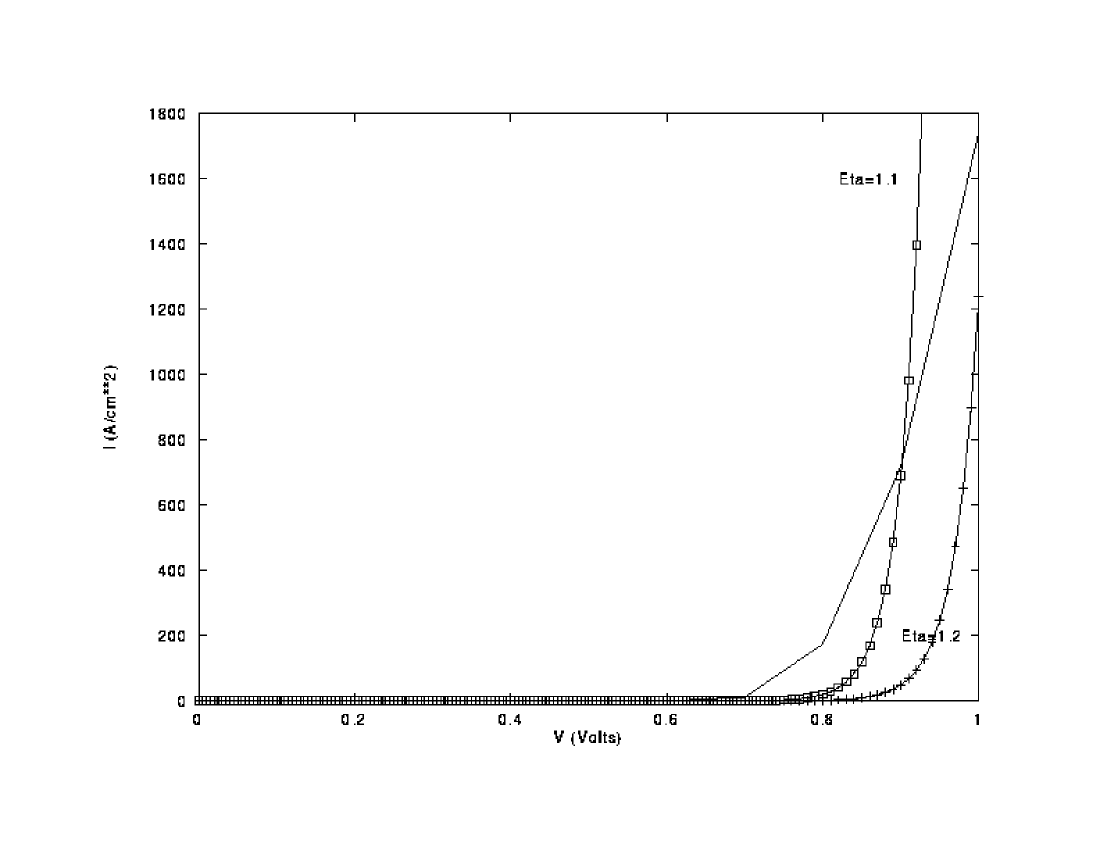
The comparison of the obtained IV characteristic to the Shockley formula is displayed in Fig. 1. The calculated characteristic falls between the two Shockley curves and in a finite current interval. This means, the general Shockley formula is not valid, within the singular perturbation approach, for arbitrary current values.
V Conclusions
The physics of the PN junction is gaining back interest with new developments in the area of nanoelectronics specially in the area of spintronics where one has to account for the spin of the carriers in addition to their charge. The usual approximations that are valid and successful in the description of the PN junction physics at the micron scale must be entirely reviewed and adapted to the nano scale. The diffusion/drift approximation as well as the nature of the singularities of the problem have been reviewed and reformulated in a way such that the underlying assumptions are revealed with their consequences.
References
- [1] M. J. Moloney, Justifying the simple diode equation, Am. J. Phys. 54, 914-916.
- [2] J. Allison, Electronic Engineering Semiconductors and Devices, Second Edition (McGraw-Hill Book Company, London, 1990), Ch. 7
- [3] J.E. Carroll, Physical Models for Semiconductor Devices, (Edward Arnold Publishers Ltd, London, 1974), Ch. 4.
- [4] R.A. Colclaser and S. Diehl-Nagle, Materials and Devices for Electrical Engineers and Physicists (McGraw-Hill, New York, 1985), Ch. 4
- [5] R.J. Elliot and A.F. Gibson, An Introduction to Solid State Physics (The Macmiilan Press Ltd., London, 1982), Ch. 9.
- [6] A.M. Ferendeci, Physical Foundations of Solid State and Electron Devices (McGraw-Hill, New York, 1991), Ch. 8
- [7] D.A. Fraser, The Physics of Semiconductor Devices, Fourth Edition (Oxford University Press, Oxford, 1986), Ch. 3
- [8] M. Goodge, Semiconductor Device Technology (Macmillan, Publishers Ltd., London, 1983) Ch. 1
- [9] J.F. Gibbons, Semiconductor Electronics (McGraw-Hill Book Company, New York, 1966; out of print), Ch.6
- [10] P.E. Gray and C. Searle, Electronic Principles (John Wiley and Sons, Newy York, 1967; out of print), Ch.4.
- [11] P.E. Gray, D. DeWitt, A.R. Boothroyd, J.F. Gibbons, Physical Electronics and Circuit Models of Transistors (John Wiley and Sons, Newy York, 1964; out of print), Ch.2 and Appendix B.
- [12] A.S. Grove, Physics and Technology of Semicopnductor Devices (John Wiley and Sons, Newy York, 1967; out of print), Ch. 3.
- [13] K. Lonngren, Introduction to Physical Electronics (Allyn and Bacon Inc, Boston, 1988), Ch. 6
- [14] D.H. Navon, Semiconductor Microdevices and and Materials (Holt, Rinehart and Winston, New York, 1986) Ch. 6
- [15] D.A. Neamen, Semiconductor Physics and Devices (Irwin, Boston, 1992), Ch. 7
- [16] D.L. Pulfrey and N.G. Tarr, Introduction to Microelectronic Devices (Prentice Hall, Englewood Cliffs, NJ, 1989) Ch.6
- [17] J. Seymour, Electronic Devices and Components (Pitman Publishing Ltd., London, 1981), Ch. 3
- [18] M. Shur, Physics of Semiconductor Devices (Prentice Hall, Englewood Cliffs, NJ, 1990) Ch. 2
- [19] L. Solymar and D. Walsh Lectures on the Electrical Properties of Materials, Fourth Edition (Oxford University Press, Oxford, 1988), Ch.9
- [20] B.G. Streetman, Solid State Electronic Devices, Third Edition
- [21] E. S. Yang, Fundamentals of Semicodnuctor Devices (McGraw-Hill, New York, 1978), Ch. 4
- [22] L.B. Valdes, The Physical Theory of Transistors (McGraw-Hill Book Company, US, 1961; out of print), Ch.9
- [23] A. van der Ziel, Solid State Physical Electronics, Second Edition (Prentice-Hall Inc., Englewood, NJ, 1968; out of print) Ch. 15.
- [24] F.F.Y. Wang, Introduction to Solid State Electronics Second Edition, (North Holland - Elsevier Science B.V., Amsterdam, 1989), Ch. 14.
- [25] S. Wang, Fundamentals of Semiconductor Theory and Device Physics (Prentice Hall, Englewood Cliffs, NJ, 1989) Ch. 2
- [26] M. Zambuto, Semiconductor Devices (McGraw-Hill, New York, 1989), Ch. 6.
- [27] S.M. Sze, Semiconductor Devices (John Wiley and Sons, Newy York, 1985), Ch.3.
- [28] S.M. Sze, Physics of Semiconductor Devices, Second Edition (John Wiley and Sons, New York, 1981), Ch. 2
- [29] M.S. Tyagi, Introduction to Semiconductor Materials and Devices (John Wiley and Sons, New York, 1991), Ch. 7
- [30] S.J Polak, C. Den Heijer, W.H.A. Schilders and P. Markowich: ”Semiconductor Device Modeling from the numerical point of view” Int. J. for Num. Methods in Engineering, Vol 24, 763-838 (1987).
- [31] C. A. Ringhofer and C. Schmeiser: ”A modified Gummel Method for the basic Semiconductor Equations” IEEE Transactions CAD Vol7, 251-253 (1988).
- [32] M. S. Mock:”On the convergence of Gummel’s numerical algorithm” Solid-State Electronics, Vol 15, 1-4 (1972).
- [33] C. P. Please:”An analysis of Semiconductor PN junctions” IMA Journal of Applied Mathematics, Vol 28, 301-318 (1982).
- [34] D. L. Scharfetter and H.K. Gummel:”Large-Signal Anlysis of a Silicon Read Diode Oscillator” IEEE Transactions ED-16, 64-77 (1969).
- [35] Y. He and G. Cao:”A generalized Scharfetter-Gummel method to eliminate Cross-Wind effects” IEEE Transactions CAD-10, 1579-1582 (1991).
- [36] A. De Mari:”An accurate numerical steady-state one dimensional solution of the PN junction”Solid State Electron ics, Vol 11, 33-58 (1968).
- [37] V. Arandjelovic:”Accurate Numerical Steady-State solutions for a diffused one dimensional junction diode”, Solid State Electron ics, Vol 13, 865-871 (1970).
- [38] P. Markowich and C. A. Ringhofer:”A Singularly Perturbed boundary value problem modelling a semiconductor device” SIAM J. Appl. Math. Vol 44, 231-256 (1984).
- [39] U.M. Ascher, R.M. Mattheij and R. D. Russel:”Numerical Solution of Boundary Value Problems for Ordinary Differential Equations”, Prentice-Hall (Englewood Cliffs).
- [40] P. Markowitch and C. Schmeiser: ”Uniform asymptotic representation of solutions of the basic semiconductor-device equations” IMA Journal of Applied Mathematics, Vol 36, 43-57 (1986).
- [41] U.M. Ascher and R. Weiss:”Collocation for singular perturbation problems I: First-order systems with constant coefficients” SIAM J. Num. Analysis Vol 20, 537-557 (1983).
- [42] P. Markowich and C. A. Ringhofer:”Collocation methods for boundary value problems on ’long’ intervals” Math. Comp. Vol 40, 123-150 (1983).
VI Tables
| AUTHOR | REF. | SEMIQUANTITIVE DRIFT ANALYSIS | FIELD IN NEUTRAL REGIONS | MAJORITY CARRIER CONCENTRATION | COMMENT |
| Zambuto zambuto | Ch. 6 | Qualitative | Not discussed | Not shown | Undergraduate |
| Yang yang | Ch. 4 | Qualitative | Not discussed | nn(x)=pn(x) | Undergraduate |
| Elliott and Gibson elliott | Ch. 9 | None | Not discussed | nn shown constant | Undergraduate |
| Fraser (UK)fraser | Ch. 3 | None | Not discussed | nn shown constant | Undergraduate |
| Seymour seymour | Ch. 3 | None | Not discussed | Not shown | Undergraduate |
| Streetman streetman | Ch. 5 | Some (Example 5.4) | Mentioned but not discussed | Not shown | Undergraduate |
| Valdes valdes | Ch. 9 | Yes | Discussed | nn(x)=pn(x) | Out of print / Undergraduate |
| Sze sze85 | Ch. 3 | None | Not discussed | Not clear | Undergraduate |
| Carroll (UK) carroll | Ch. 4 | None | Mentioned but not discussed | Not clear | Undergraduate |
| Solymar and Walsh (UK) solymar | Ch.9 | None | Not discussed | nn(x)=pn(x) implied | Undergraduate |
| Shur shur | Ch. 2 | Some (Fig. 2.3-8) | Not discussed | nn(x)=pn(x) implied | Senior UG / Graduate level |
| Pulfrey and Tarr (Canada) pulfrey | Ch. 6 | None | Not discussed | nn(x)=pn(x) implied but nn=constant in diagrams | Undergraduate |
| Colclaser and Diehl-Nagle colclaser | Ch. 7 | None | Not discussed | Not mentioned and not shown | Undergraduate |
| Navon navon | Ch. 6 | None | Not discussed | nn(x)=pn(x) in diagram | Undergraduate |
| Sze sze81 | Ch. 2 | None | Not discussed | Not clear | Senior Undergraduate / Graduate |
| Wang swang | Ch. 14 | None | Not discussed | Inferred | Senior Undergraduate |
| Goodge (UK) goodge | Ch.1 | None | Not discussed | nn(x)=pn(x) in diagram | Undergraduate |
| Grove grove | Ch.3 | None | Not discussed | Not clear | Out of print / Undergraduate |
| Van Der Ziel ziel | Ch. 15 | None | Not discussed | Not clear | Out of print / Undergraduate |
| Lonngren lonngren | Ch. 6 | None | Not discussed | Not discussed | Undergraduate |
| Tyagi tyagi | Ch. 7 | Qualitative | Mentioned but not discussed | nn(x)=pn(x) (Fig.7.3) | Undergraduate |
| Gibbons gibbons | Ch. 6 | Yes | Discussed | nn(x)=pn(x) | Out of print / Undergraduate |
| Ferendeci ferendeci | Ch. 8 | None | None | Not clear | Undergraduate |
| Allison allison | Ch. 7 | None | None | Not clear | Undergraduate |
| Neamen neamen | Ch. 8 | Some | E estimated | Not clear | Undergraduate |
| F. Wang fwang | Ch. 8 | None | None | Not clear | |
| Gray et al. gray64 | Ch.2 and App. B. | Some | Yes | nn(x)=pn(x) in diagram | Out of print / Undergraduate |
| PROPERTY / PARAMETER | TYPICAL VALUE | COMMENT |
|---|---|---|
| Permittivity | 11.9 | |
| Intrinsic concentration, ni, cm-3 | 1.51010 | |
| Donor concentration, ND, cm-3 | 51015 | |
| Acceptor concentration, NA, cm-3 | 1019 | p+-n junction |
| Equilibrium hole concentration in n-region, pn0, cm-3. | 4.50104 | |
| Equilibrium electron concentration in p-region, np0, cm-3. | 22.5 | |
| Hole recombination time in n-region, , s | ||
| Electron recombination time in p-region, s | ||
| Electron drift mobility in the n-region, cm2V-1s-1. | ||
| Hole drift mobility in n-region, cm2V-1s-1 | ||
| Electron drift mobility in the p-region, cm2V-1s-1. | ||
| Hole drift mobility in p-region, cm2V-1s-1. | ||
| Electron diffusion coefficient in n-region, Den, cm2.s-1 | 33.55 | |
| Hole diffusion coefficient in n-region, Dhn, cm2.s-1 | 11.73 | |
| Electron diffusion coefficient in p-region, Dep, cm2.s-1 | 2.73 | |
| Hole diffusion coefficient in p-region, Dhp, cm2.s-1 | 1.68 | |
| Electron diffusion length in n-region, Len, cm | 3.9010-3 | Len= |
| Hole diffusion length in n-region, Lhn, cm | 2.3110-3 | |
| Electron diffusion length in p-region, Lep, cm | 8.2410-5 | |
| Hole diffusion length in p-region, Lhp, cm | 6.4610-5 | |
| Builtin potential, Vbi, V | 0.854 | |
| Ebi, V.cm-1 | 3.60104 | No bias |
| Width, W, of depletion region, cm | 4.74110-5 | On n-side. Much shorter than hole diffusion length on n-side. |
| Width, Wn, of depletion region in n-side, cm | 4.73910-5 | Much shorter than hole diffusion length in n-region. |
| Width, Wp of depletion region in p-side, cm | 2.36910-8 | Much shorter than electron diffusion length in p-region |
| Length of n-side | 2.3110-2 | 10Lh Long diode |
| Length of p+-side | 8.2410-4 | 10LeLong diode |
| FORWARD BIAS, V | 0.55 | |
| Built-in electric field, V.cm-1 | 2.15104 | Smaller than zero bias case |
| Width, W, of depletion region at 0.55V, cm | 2.8310-5 | On n-side. Narrower under forward bias. Much shorter than hole diffusion length on n-side. |
| pn(0), injected hole concentration at x=0 | 7.811013 | |
| np(0), injected electron concentration at x’=0 | 3.911010 | |
| pn(0)/ND | 0.0156 | 1.56%, small injection. At V=0.60V, this becomes 11% |
| np(0)/NA | 3.9110-9 | Extremely small injection |
| J0h, A.cm-2 | 3.66310-11 | |
| J0e, A.cm-2 | 1.19510-13 | |
| J0, A.cm-2 | 3.67510-13 | J0h |
| J0.55, A.cm-2 | 0.0638 | |
| En×, V.cm-1 | 0.0613 | Field in n-region far away from junction |
| Enmax, V.cm-1 | 0.1749 | Field just outside SCL |
| Enmax/Ebi | 8.1310-6 | |
| Vnat V=0.55V | 0.00168 | Very small, Vnis 0.3% of bias |
| Vnat V=0.60V | 0.0116 | Vnis 12.3% of bias |
| Epmax = Ep×, V.cm-1 | 6.110-4 | Field far away from junction |
| Epmax/Ebi | 2.810-8 | Extremely small |
| Vp | 5.0410-7 | Extremely small, |
| JUST OUTSIDE SCL ON n-SIDE, x=0 | ||
| Majority drift current, A.cm-2 | 0.1820 | Largest magnitude in positive direction |
| Majority diffusion current, A.cm-2 | -0.1818 | Opposite direction, about the same magnitude as majority drift |
| Minority drift current, A.cm-2 | 0.001 | Smallest magnitude |
| Minority diffusion current, A.cm-2 | 0.06359 | About a third of the magnitude of majority drift. |
| JUST OUTSIDE SCL ON p-SIDE, x’=0 | ||
| Majority drift current, A.cm-2 | 0.06351 | Largest magnitude. Dominates conduction. |
| Majority diffusion current, A.cm-2 | -0.000891 | Opposite direction |
| Minority drift current, A.cm-2 | 2.3310-19 | Smallest magnitude-virtually zero |
| Minority diffusion current, A.cm-2 | 0.00255 | Next largest magnitude |