PHOTONIC CRYSTAL LASER ACCELERATOR STRUCTURES
Abstract
Photonic crystals have great potential for use as laser-driven accelerator structures. A photonic crystal is a dielectric structure arranged in a periodic geometry. Like a crystalline solid with its electronic band structure, the modes of a photonic crystal lie in a set of allowed photonic bands. Similarly, it is possible for a photonic crystal to exhibit one or more photonic band gaps, with frequencies in the gap unable to propagate in the crystal. Thus photonic crystals can confine an optical mode in an all-dielectric structure, eliminating the need for metals and their characteristic losses at optical frequencies.
We discuss several geometries of photonic crystal accelerator structures. Photonic crystal fibers (PCFs) are optical fibers which can confine a speed-of-light optical mode in vacuum. Planar structures, both two- and three-dimensional, can also confine such a mode, and have the additional advantage that they can be manufactured using common microfabrication techniques such as those used for integrated circuits. This allows for a variety of possible materials, so that dielectrics with desirable optical and radiation-hardness properties can be chosen. We discuss examples of simulated photonic crystal structures to demonstrate the scaling laws and trade-offs involved, and touch on potential fabrication processes.
Submitted to Particale Accelerator Conference (PAC 2003), May 12–16, 2003, Portland, Oregon (IEEE)
1 INTRODUCTION
The extraordinary electric fields available from laser systems make laser-driven charged particle acceleration an exciting possibility. Practical vacuum laser acceleration requires a guided-mode structure capable of confining a speed-of-light (SOL) mode and composed entirely of dielectric materials, and photonic crystals provide a means to achieve this capability. A photonic crystal is a structure with permittivity periodic in one or more of its dimensions. As described in [1], optical modes in a photonic crystal form bands, just as electronic states do in a crystalline solid. Similarly, a photonic crystal can also exhibit one or more photonic band gaps (PBG’s), with frequencies in the gap unable to propagate in the crystal. Confined modes can be obtained by introducing a defect into a Photonic Crystal lattice. Since frequencies in the bandgap are forbidden to propagate in the crystal, they are confined to the defect. A linear defect thus functions as a waveguide.
A significant benefit of photonic crystal accelerators is that only frequencies within a bandgap are confined. In general, higher order modes, which can be excited by the electron beam, escape through the lattice. This benefit has motivated work on matallic PBG structures at RF frequencies [2]. In addition, an accelerating mode has been found in a PBG fiber structure [3]. After discussing 2D planar structures we consider the fiber geometry in more generality.
2 2D PLANAR PHOTONIC CRYSTAL ACCELERATOR STRUCTURES
2.1 Structure Geometry
The geometries we consider in this section are two-dimensional: we take them to be infinite in the vertical () direction, while the electron beam and the accelerating optical field copropagate in the -direction, transverse to the direction of symmetry. While such structures are not immediately suitable for charged particle acceleration, 2D structures can be analyzed with much less CPU time than can 3D structures, thereby allowing rapid exploration of multiple sets of geometric parameters. The computational technique is discussed further below.
Our underlying photonic crystal lattice is a triangular array of vacuum holes in a silicon substrate. Assuming an operating wavelength of 1.5 µm in the telecom band, silicon has a normalized permittivity of [4]. Such a lattice exhibits a wide TE bandgap, as desired since the accelerating field component is transverse to the direction of symmetry. For lattice constant the nearest-neighbor center-to-center hole spacing, we choose the hole radius to maximize the relative width of the bandgap.
The accelerator structure consists of a vacuum guide in this lattice, as shown in Fig. 1.
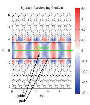
The guide width is defined such that the distance between the centers of the holes adjacent to the waveguide are . Also, dielectric material can be added to the sides of the guide, and we let denote the total width of the dielectric “pad” added to both sides of the guide. Fig. 1 also shows an accelerating mode of this geometry, i.e. is nonzero on axis and . In fact, for a general selection of and , there will be a for which this waveguide mode is synchronous. This is because the dispersion properties of this PBG waveguide are similar to a metallic guide in that throughout most of the bandgap, but at the upper edge of the gap the dispersion curve reduces in slope and meets the SOL line. The padding can be added in order to bring the SOL frequency into the center of the gap where the dispersion curve is more linear.
2.2 Accelerating Mode Parameters
Several parameters characterize the performance of an accelerating mode. The relationship between the input laser power and the accelerating gradient is described by the characteristic impedance [5]. Since our 2D structures only confine modes in one transverse dimension, we normalize the impedance to that of a structure one wavelength high, so , where is the accelerating gradient and is the laser power per unit height. We find an empirical power-law scaling of the impedance, with .
Next, there is the damage factor , where is the maximum electric field magnitude anywhere in the dielectric material. Since laser power is ultimately limited by the damage threshold of the material, the damage factor is an important measure of the maximum possible accelerating gradient a structure can sustain.
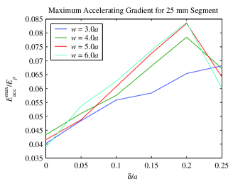
The damage threshold exhibits a dependence on laser pulse width which becomes favorable at very short pulse widths, as examined in [6] and paramaterized in [5]. Thus these accelerator structures are transmission-mode, and a high group velocity is desired so that short pulses may be used. The qualitative behavior of these parameters presents a trade-off. As the guide is widened, the damage factor decreases. On the other hand, the group velocity increases, allowing shorter laser pulses to be used, for which the material damage threshold is at a higher field. To find the optimum parameters we plot the maximum possible accelerating gradient taking both effects into account in Fig. 2.
3 PHOTONIC CRYSTAL FIBER STRUCTURES
The geometry of this structure is again a triangular array of vacuum holes, this time in silica (). Here the structure is considered to be a fiber drawn infinitely in the beam propagation direction, with the electrons and laser pulse copropagating along the fiber. For these structures , and the defect consists of a larger central hole. Modes were found for three different mode radii, and are shown in Fig. 3.
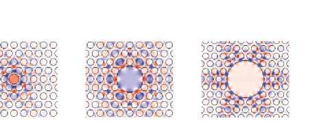
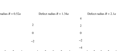
The frequencies of the three modes are given by of 8.20, 8.12, and 8.20 and group velocities , , and (left to right).
The structure was simulated using periodic boundary conditions, and the fields in the lattice region are due to crosstalk between neighboring defects. By increasing the size of the supercell, this crosstalk can be minimized, however the computational time significantly increases. Also, the 6-fold azimuthal symmetry of the structure implies that SOL modes in vacuum contain only azimuthal modes for an integer, reducing the emittance blowup from higher-order modes. Finally, we find that the characteristic impedance decreases with guide radius, as is the case with metallic waveguide structures.
4 COMPUTATION TECHNIQUES
We use the MIT Photonic Bands (MPB) package, a public-domain code using an iterative eigensolver technique [7]. For a given geometry and Bloch wavevector, MPB computes frequencies and field configurations of supported modes. MPB can compute group velocities of modes as well by applying the Feynman-Hellmann theorem [8, 9].
Using the frequencies and group velocities, we can inductively converge on the longitudinal wavenumber for which a speed-of-light mode exists. Having found a mode for a particular wavenumber, we can use its frequency and group velocity to obtain a linear approximation for its dispersion curve near that wavenumber. The intersection of that approximation with the SOL line gives the wavenumber for the next computation, which yields a mode whose phase velocity is closer to . Since the iterative eigensolver for each step can be seeded with the field configuration from the result of the previous step, successive steps are quite fast, and convergence to an SOL mode is a computationally light task once the initial mode has been found.
5 FABRICATION POSSIBILITIES
The 2D structures discussed above are amenable to photolithography, with 50 : 1 apect ratios available from current reactive ion etching equipment. Some investigation into fabrication of these structures has taken place in the past [10]. Fabrication of 3D photonic crystals with omnidirectional bandgaps, such as the “woodpile” structure [11], is an active area of research. A number of techniques are being developed, including multilayer lithography, wafer fusion, stacking by micromanipulation, self-assembly, and others [12]. PCF manufacturing is a large and growing area of research in industry, since photonic crystals allow for tailoring optical properties to specific applications, from nonlinearity for wavelength conversion in telecommunications to large mode area for materials processing [13].
6 CONCLUSION
Photonic crystals have great promise as potential laser accelerator structures. Not only do they support accelerating modes, but such modes exist for a wide range of geometric parameters. While the basic accelerator parameters have been examined, much remains to be done to understand the properties of these structures. Wakefield computations as well as coupling structure design have yet to be explored. In addition, there are many photonic crystal lattices for which accelerating modes have not been computed, including 3D geometries. However, manufacturing technology, numerical simulation capability, and theoretical understanding continue to progress at an extraordinary rate, driven by industry forces. We therefore expect a bright future for photonic crystals as an accelerator technology.
References
- [1] J. D. Joannopoulos, R. D. Meade, and J. N. Winn, Photonic Crystals: Molding the Flow of Light (Princeton University Press, Princeton, NJ, 1995).
- [2] M. A. Shapiro et al., Phys. Rev. ST Accel. Beams 4, 042001 (2001).
- [3] X. E. Lin, Phys. Rev. ST Accel. Beams 4, 051301 (2001).
- [4] D. F. Edwards, in Handbook of Optical Constants, edited by E. D. Palik (Academic Press, 1985), vol. 1, p. 547.
- [5] L. Schächter, R. L. Byer, and R. H. Siemann, in Advanced Accelerator Concepts: Tenth Workshop, Mandalay Beach, CA, 2002, edited by C. E. Clayton and P. Muggli, U.S. Department of Energy (American Institute of Physics, Melville, NY, 2002), no. 647 in AIP Conference Proceedings, pp. 310–323.
- [6] B. C. Stuart et al., Phys. Rev. Lett. 74, 2248 (1995).
- [7] S. G. Johnson and J. D. Joannopoulos, Optics Express 8, 173 (2001).
- [8] See for instance J. J. Sakurai, Modern Quantum Mechanics, Rev. ed. (Addison-Wesley, Reading, MA, 1995)
- [9] S. G. Johnson et al., Phys. Rev. E 65, 066611 (2002).
- [10] Wendt et al., J. Vac. Sci. Technol. B 11, 2637 (1993).
- [11] S. Y. Lin et al., Nature 394, 251 (1998).
- [12] S. G. Johnson, Fabrication of Three-Dimensional Crystals: Those Clever Experimentalists, from lecture series Photonic Crystals: Periodic Surprises in Electromagnetism, http://ab-initio.mit.edu/photons/tutorial/
- [13] René Engel Kristiansen, Guiding Light with Holey Fibers, OE Magazine June 2002, p. 25.