A two dimensional position sensitive gas chamber with scanned charge transfer readout
Abstract
We have constructed and tested a 2d position sensitive parallel-plate gas ionization chamber with scanned charge transfer readout. The scan readout method described here is based on the development of a new position dependent charge transfer technique. It has been implemented by using gate strips perpendicularly oriented to the collector strips. This solution reduces considerably the number of electronic readout channels needed to cover large detector areas. The use of a 25m thick kapton etched circuit allows high charge transfer efficiency with a low gating voltage,consequently needing a very simple commutating circuit. The present prototype covers 88 cm2 with a pixel size of mm2. Depending on the intended use and beam characteristics a smaller effective pixel is feasible and larger active areas are possible. This detector can be used for X–ray or other continuous beam intensity profile monitoring.
keywords:
Gas ionization chamber , Position sensitive detector , Scan readoutPACS:
29.40.Cs , 29.40.Gx , 07.85.Fv, , , , , , , ,
1 Introduction
To monitor high rate beam fluency gas ionization chambers based devices [1] can be used. In order to obtain a 2d profile of radiation dose or fluency it is necessary to have a highly segmented anode [2] [3]. This represents a major problem when the size of the chamber is large compared with the anode segmentation pitch. In the present work we describe a new and simple solution developed to give real two dimensional readout on a gas ionization chamber. The method consists on scanning electronically the detector active area in the perpendicular direction to the readout strips orientation (strips instrumented with the measuring electro-meters). Gated charge transfer is a well known method which has been used in different radiation detectors like, for example, gated gas-filled Time Projection Chambers [4] in High Energy Physics.
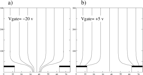
The transfer of electrons drifting from the detector volume to the collector electrode strips can be blocked by means of a local electric field that dominates the drift field in the proximity of the gate electrode strips (see simulation in Figure 1). In this way we provide a single stage control of the charge transfer from the gas drift region to the collector electrodes. In this work we profit from the great development of Micro–Pattern Gas Detectors (MPGD) [5] in the last years, specially the advances on kapton etching techniques. In our case we integrated a gating grid using a two metal layer circuit based in a kapton foil glued on a FR4 epoxy substrate to provide mechanical rigidity. The use of a 25m thick kapton foil to produce a two level readout circuit allows to use a small gating voltage.
2 Prototype description
To design and optimize the geometry of the gate and collector electrodes we simulated the electric field map of a transfer gap cell through MAXWELL3D111Ansoft Corporate, Pittsburgh USA and MATLAB222The MathWorks, Inc. 3 Apple Hill Drive, Natick MA(USA) 01760-2098 programs. For the final design it was chosen a 1:2:1 ratio corresponding to the transfer gap height:gate–spacing:gate–width. With this geometry we expected to have a low electron transfer transparency (well bellow 1%) using a relatively low positive (+5V) ”closed gate” voltage333In the present work collector electrodes are always grounded. and moderate drift fields ( V/m). A wider gate strip spacing would increment the electron transparency for a given negative ”open gate” voltage, but also higher positive voltages would be needed to block efficiently the electron drift. On the other hand the local electric field present around the gate strip either in open or closed mode should not affect significantly the electric field in the drift region. This is another important reason to use a small transfer gap between the gate and collector strips.

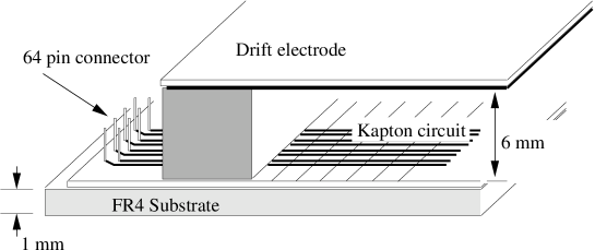
The readout circuit layout of this prototype is described in Figure 2. We used a 25m thick kapton foil metal coated on both sides with 5m copper. After etching of the copper, we obtained 35m wide and 1 mm wide strips on the gate and collector plane respectively. The foil was glued on a 1mm FR4–epoxy substrate and subsequently kapton in the gap between gate strips was removed obtaining the Figure 2 micro-pattern. In order to provide a simple connection procedure a 64 pin 1/10 inch pitch standard connector was included in the board edge design for both gate and collector strips. This choice implies a 1.27 mm pitch in the detector active area. The collector strips were thus made 1mm wide with 1.27 pitch while 17 gate strips were joined in a group in the detector edge to achieve the previous effective pitch. The drift gas gap was built using a G10 6mm height frame glued on the readout board, and this volume was closed with a drift electrode made of 200m thick G10 copper clad on one side.
3 Charge transfer
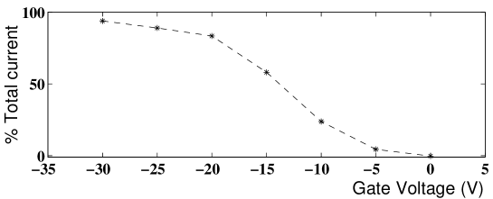
The experimental transparency for electrons obtained as a function of the gate voltage is shown in Figure 4. This measurements were done using pure Ar at atmospheric pressure, and corresponds to the ratio of the ionization current under X–ray irradiation measured at the collector and at the drift electrode. The plot shows that very small transparency values () can be obtained for low positive voltages at ”closed mode”. The transparency increases when applying negative voltages at the gating electrodes, showing that there is a transition region centered on -15V, and can reach values very close to 1 (”open mode”) when the gate voltage is below -20V. If the drift field is increased, the gate voltage has also to be increased proportionally to maintain the same transparency value. The fraction of current produced by electrons arriving to the gate electrode is the complementary value of the transparency calculated for the collector. We have chosen -17V as open gate voltage as this value can be commutated using standard CMOS analogue switches. If we consider the width of the gate strips (35 m in Figure 2) and the corresponding space between gate strips (40 m in Figure 2), the expected electron transparency is equal to the optical limit defined by
being and the gate and drift voltages respectively, the height of the gate strips over the collector electrodes and the gas gap below the drift electrode. The measured maximum transparency significantly deviates from this expectation due to the trapezoidal etching of the kapton layer that partially covers the collector electrodes in the space between gate strips.
4 Two dimensional readout
To demonstrate the working principle of our position sensitive charge transfer scan readout method, a small area of the prototype was instrumented with charge integration electronics. To drive the detector, two separate electronic boards were used, one with the commutation circuit to sequentially commutate from closed to open gate voltage on the gate strips and another board with the necessary electronic readout channels to integrate the charge collected by each individual collector strip (integrators board). To integrate the collector current we used a precision switched IVC102 [6] integrating amplifier (with an internal feedback capacitor set to 10 pF).
To sequentially change the voltage value applied to each gate strip a shift register was used, built by means of daisy chained D–type flip–flops (HEF40174B) whose outputs were connected to double analogue switches (AD7592DI). These analogue switches commute from closed gate voltage value (that keeps the electron transparency at lowest values), to a negative open gate voltage value giving a high electron transparency for the selected gate strip (typically 70% in our setup). A scheme of the readout circuit is shown on Figure 5. For the synchronous control of the two electronic boards we used a personal computer PCI embedded card444National Instruments PCI-6023E DAQ card..
The first prototype was instrumented with a total number of 96 effective pixels (on an active area of 15.2 10.2 mm2), corresponding to 12 gate channels and 8 collector channels. The total capacitance at the detector between gate and collector plane is 7nF, meaning a 2pF capacity per pixel. This gate–collector capacity gives a 2s transient time during commutation, considering the 3k impedance of the IVC102 (with switches S1+S2 closed). This dead time is small compared with the typical integration times used (of the order of milliseconds). The total time required to obtain an image is equal to the integration time needed to integrate the charge transfered by each gate strip times the number of gate strips.
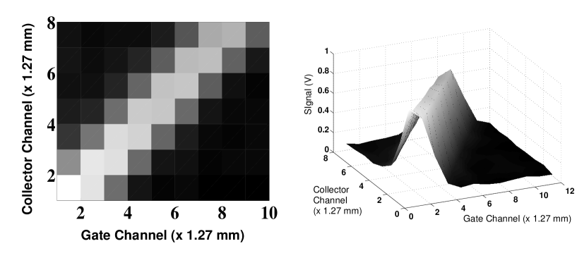
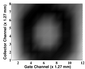
Figure 6 and 7 show two X–ray images obtained with this prototype using a Chromium X–ray tube: a 1.5 mm slit between two 5mm thick aluminum plates and a 5mm screw nut were illuminated. The and gate voltage values used were +5V and -17V respectively, and the drift field applied in the image was 1.7104 V/m in pure Ar. To obtain this images a scan readout cycle time of less than 10 seconds was required, with a collector current value of 7 pA in the pixels with maximum signal.

The charge transparency value when the gate electrode is set to the closed state should be ideally zero. But the real value differs from zero by a small amount ( 0.1%). This causes a leakage current, of a value proportional to the detector area, that can seriously distort the image. Nevertheless, if the leakage current per effective pixel is small we can correct this effect by what we have called differential readout. The correction term is measured by integrating the detector current during the same time interval used for the standard readout with all the gate electrodes closed.
This value will then be subtracted as a pedestal from the values obtained with the gate electrodes on opened state. In this way the image will not be dramatically affected by the non zero transparency value at the closed gate state.
5 Conclusions
We have proved the working principle of a simple and reliable readout method for 2d position sensitive gas ionization detectors. This two dimensional charge transfer readout solution allows to cover large detector areas giving a high number of effective pixels and minimizing the number of readout electronic channels. By using a kapton–insulated two layer readout circuit, charge transfer does not affect the drift field and the control of the charge transfer process can be done with very low voltage values. The detector can be used not only with gases but with other photo-conductive media like non–polar liquids ( isooctane or tetrametilsilane). For low beam intensity or fast readout cycle applications, an intermediate gas avalanche device, like a Gas Electron Multiplier [7], can be added to improve its sensitivity. Considering moderate gas gains around 100, an image could be readout with a cycle period 100 times faster than an equivalent ionization chamber, leading to a fast beam imaging device.
6 Acknowledgments
We are grateful to Manuel Sanchez from CERN EST/DEM group for his permanent technical support and collaboration.
References
- [1] S.N. Ahmed, H.-J. Besch, A.H. Walenta, N. Pavel and W. Schenk, Nucl. Instr. and Meth. A 449(2000) 248
- [2] V.K. Myalistin, H.-J. Besch, H.W. Schenk and A.H. Walenta, Nucl. Instr. and Meth. A 323(1992) 97
- [3] H.J. Besch, E.J. Bode, R.H. Menk, H.W. Schenk, U. Tafelmeier, A.H. Walenta and H.Z. Xu, Nucl. Instr. and Meth. A 310(1991) 446
- [4] The ALEPH collaboration, Nucl. Instr. and Meth. A 294(1990) 121
- [5] F. Sauli, A. Sharma, Ann. Rev. Nucl. Part. Sci. 49 (1999) 341
- [6] Precision switched integrator transimpedance amplifier. Data sheet, Burr–Brown, USA 2000.
- [7] S. Bachmann, A. Bresan, S. Kappler, B. Ketzer, M. Deutel, L. Ropelewski, F. Sauli, E. Schulte Nucl. Instr. and Meth. A 471(2001) 115