The STAR Silicon Strip Detector (SSD)
Abstract
The STAR Silicon Strip Detector (SSD) completes the three layers of the Silicon Vertex Tracker (SVT) to make an inner tracking system located inside the Time Projection Chamber (TPC). This additional fourth layer provides two dimensional hit position and energy loss measurements for charged particles, improving the extrapolation of TPC tracks through SVT hits. To match the high multiplicity of central Au+Au collisions at RHIC the double sided silicon strip technology was chosen which makes the SSD a half million channels detector. Dedicated electronics have been designed for both readout and control. Also a novel technique of bonding, the Tape Automated Bonding (TAB), was used to fullfill the large number of bounds to be done. All aspects of the SSD are shortly described here and test performances of produced detection modules as well as simulated results on hit reconstruction are given.
1 Introduction
The STAR Silicon Strip Detector (SSD) [1] constitutes the fourth layer of the inner tracking system. Installed between the Silicon Vertex Tracker (SVT) and the Time Projection Chamber (TPC), the SSD will enhance the tracking capabilities of the STAR experiment by measuring accurately the two dimensional hit position and energy loss of charged particles. It aims specifically at improving the extrapolation of TPC tracks through SVT hits and increasing the average number of space points measured near the collision thus increasing the detection efficiency of long-lived meta-stable particles.
The SSD is placed at a distance of 230 mm from the beam axis, covering a pseudo-rapidity range of which leads to a total silicon surface close to 1 .
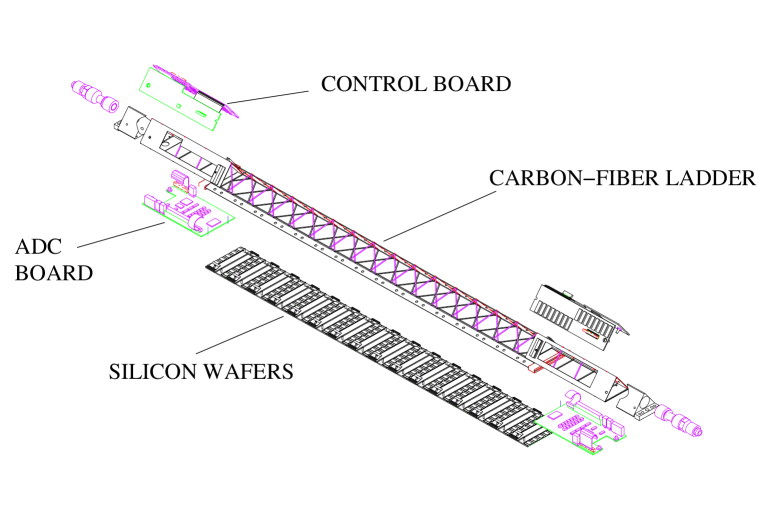
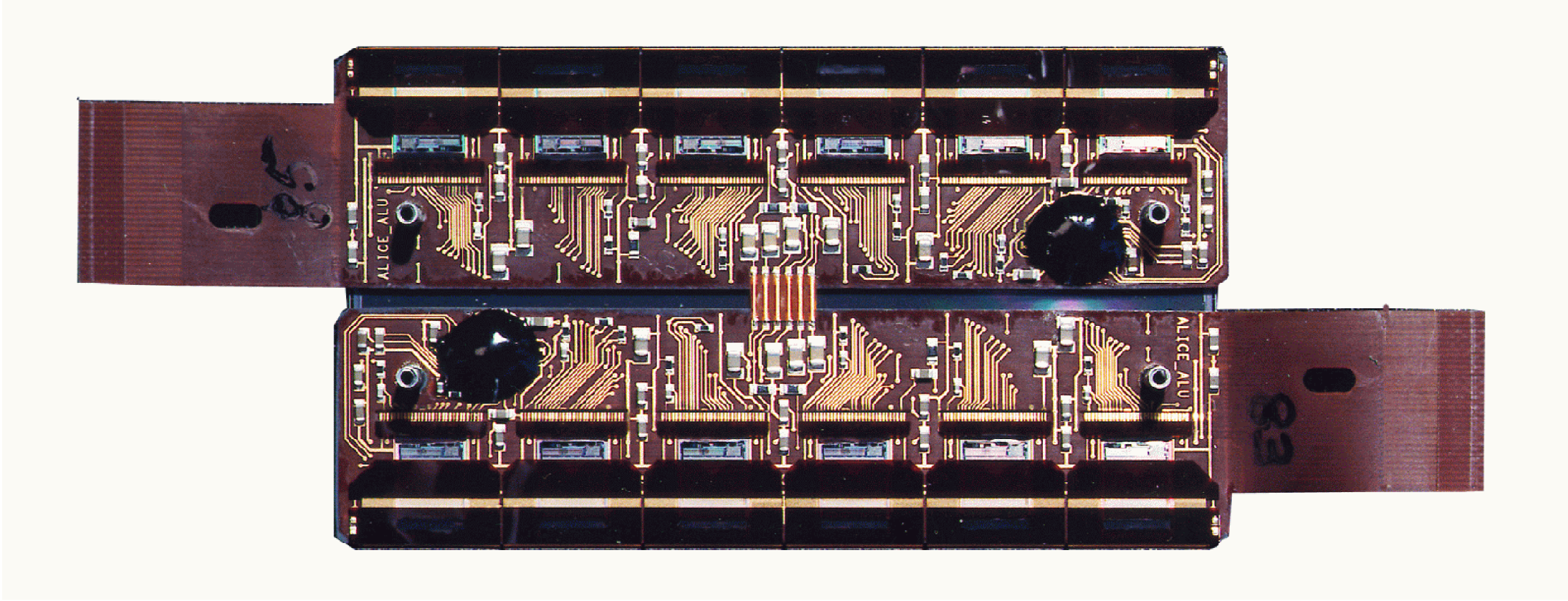
The design of the SSD is based on two clamshells, each containing 10 carbon-fiber ladders. Each ladder (figure 1) supports 16 wafers using double-sided silicon strip technology (768 strips per side) and connected to the front-end electronics (6 ALICE 128C chips per side) by means of the Tape Automated Bonded (TAB) technology [2]. The ladders are tilted with respect to their long axis, allowing the overlap of the detectors in the transverse plane for better hermiticity and alignment performances. A bus cable transports the analog signals along the ladder to two 10 bits ADC boards installed at both ends. After digitization, the signals are sent to Readout Boards which are linked to the DAQ system through Giga-link optics fibers. The whole system is remotely controlled to monitor powers and temperature but also to calibrate and tune the front-end electronics. The cooling system is based on an air-flow through the ladder which is embedded in a mylar sheet. The total radiation length has been estimated to be around .
2 Mechanics
The mechanical design is constrained by : 1) the inner radius of the TPC (including a safety margin in order to avoid high voltage breaks from the TPC field cage); 2) limited material budget; 3) stability with respect to temperature variations and minimizatiuon of the sagging due the weight of the modules in order to insure good alignment precision. Each ladder is 1060 mm long, featuring a triangular cross-section of 40 mm base. The ladders are made of high-modulus carbon-fiber which allows for both a good rigidity and a low material budget. The saggita of a loaded ladder has been estimated by simulation to be lower than 100 m. The SSD modules are glued on the carbon ladder by an elastic epoxy glue in order to accomodate the different thermal expansion coefficients of silicon and carbon. Two sets of ten ladders are assembled on C-shaped ribs which allow for installation on the common SVT/SSD support structure.
3 Wafers
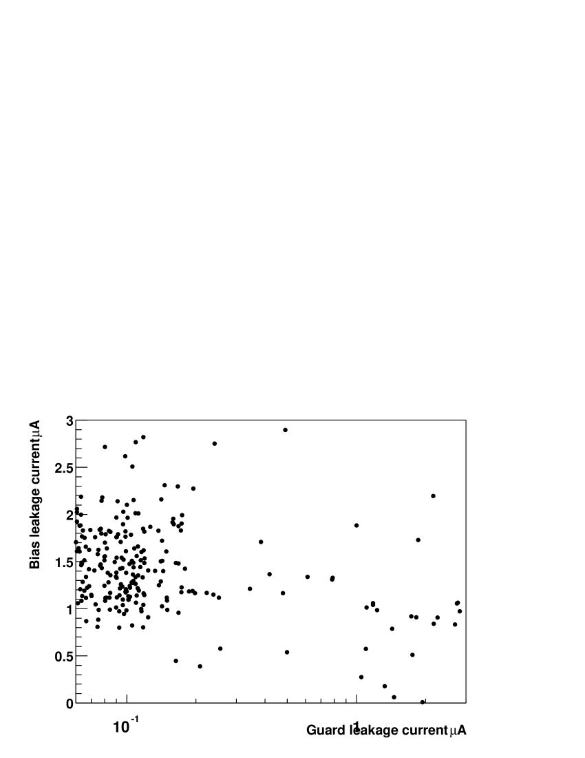
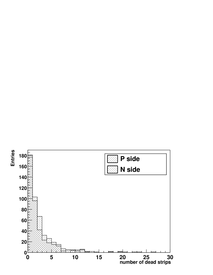
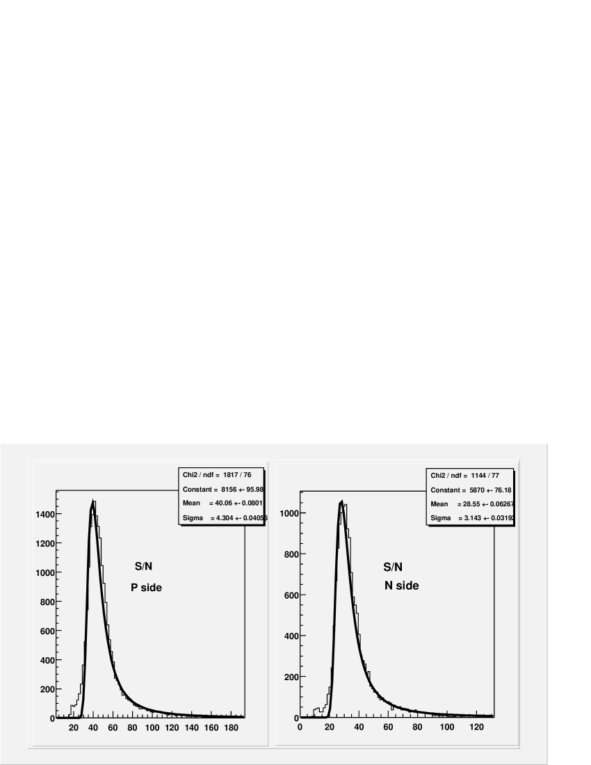
The design of the silicon wafers was inspired by the initial design of the ALICE experiment silicon strip detector [4]. The wafers are 75 mm by 42 mm sized and 300 m thick. The strips are oriented perpendicularly with respect to the longest dimension of the detector on both sides (double-sided technology), with a pitch of 95 m (768 strips per side). The insulation between strips on the N side is achieved by p-spraying, and the biasing scheme uses punch-through technology. The bias ring surrounded by a guard ring define an active area of 73 mm by 40 mm. The strips on the P and N sides are inclined by 35 mrad with respect to each other and symetrically with respect to the wafer edge. Combined with the charge correlation due to the double-sided technology, this stereo angle allows an efficient 2-dimension impact point reconstruction in a high multiplicity environment with a low ambiguity yield [5]. The pitch is chosen in order to achieve a minimum resolution (digital resolution) of 30 m in the transverse plane and m along the Z axis. During production, all the 440 detectors were fully characterized with a probe-station allowing the measurement of their depletion voltage and leakage current (figure 2). The detectors can currently be operated between 20 V and 50 V. Moreover, the corresponding 680000 strips have been scanned to identify every defective strips [10]. A very low average number of dead strips have been measured, well below , see figre 3. Prototypes were irradiated in order to test their capability to cope with the expected fluxes [7].
4 Front-end electronics and modules
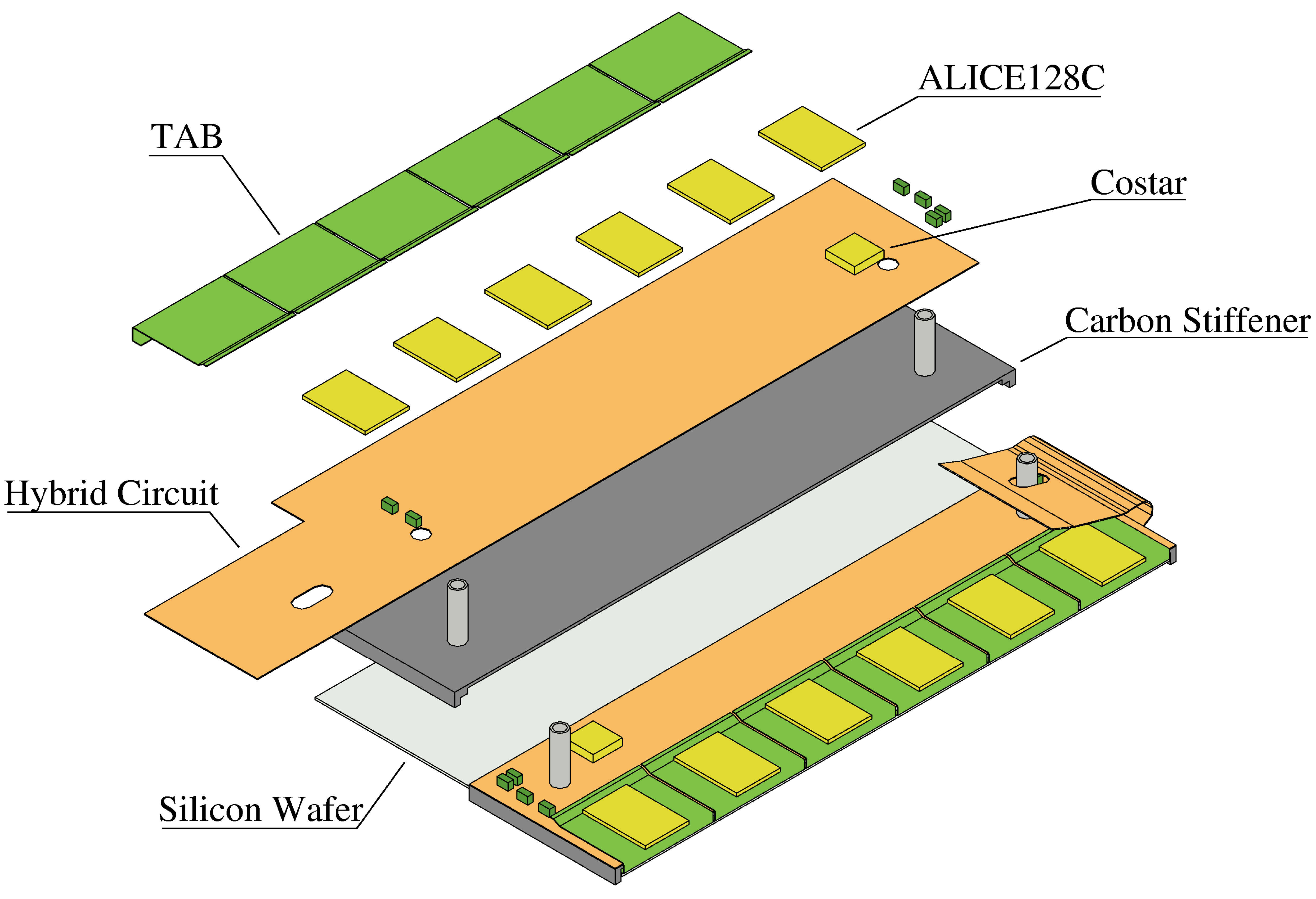
Each of the 320 detection modules (figure 4) is composed of a silicon wafer,two hybrid circuits (one per side) supporting the front-end electronics and a mechanical structure [3]. The front-end electronics is constituted by six ALICE 128C chips per side [8]. The ALICE 128C is a low power chip, specially designed for the STAR and ALICE silicon strip detectors using the AMS 1.2 m CMOS technology. Each of the 128 analog input channels of the chips allows the amplification, shaping and storage of the charge collected on a single strip. The shaping time is adjustable between 1.2 and 2 s, the dynamic range extends up to 13 MIPs ( signals collected on each side of the wafer have different polarity) with a nominal noise of 290 + 8 . An analog mutiplexer allows the sequential readout of the data at a rate up to 10 MHz.The chip is controlled through JTAG protocol in order to tune and monitor remotely its performance. The front-end electronics is supported by a hybrid circuit which is a copper printed kapton tape glued on a carbon stiffener. The main components on the hybrids are ALICE128C chips and a COSTAR (COntrol STAR) chip [9] designed for slow control purposes : temperature and leakage current measurements as well as pedestal compensation. Tape Automated Bonding (TAB) is used for the connection between the strips on the detector and the analog inputs of the ALICE 128C chips [12]. This bumpless technology is based on a kapton microcable on which are printed copper strips, the flexibility of the cable allowing the folding of the hybrids on top of the detector in order to make the detection module very compact, see figure 5. Furthermore, this cable plays the role of a pitch adaptator between the 95 m pitch of the detector and the m pitch of chips on the hybrid. The TAB technology is also used for the connection between the chip and the hybrid. During the production stage, the chip is first connected to a TAB tape and then fully tested [10] before its connection to the detector. An internal pulser permits testing of all channels individually both during stages of assembly and on the final installation in STAR. After the assembly of modules, each strip is calibrated with a dedicated laser test bench.
5 Readout electronics
The Control Board which receives the signals from the modules and also takes care of JTAG communication and latchup protection is connected to the hybrid with a kapton cable. The analog signals are transfered from the Control Board to the ADC Board, both located at the end of the ladder (one set per side and per ladder). The ADC board reads sequentially the data of a full ladder at 10 MHz and digitizes to 10 bits. The analog signal (50 mV/MiP) spans a range of 1 V. The two piece Control Board is joined with a flex cable and folded to conform to the triangular carbon ladder. The Control Board is connected to the ADC Board which is installed at the bottom edge of the ladder. The interface between the detector (ADC, JTAG control of the chips) and the STAR system (DAQ, Slow-control, trigger) is done through four Readout Boards located on the TPC wheels. All the functionalities of the Readout Board are performed by an FPGA programable chip. The system is able to read all the channels in less than 5 ms.
6 Performances
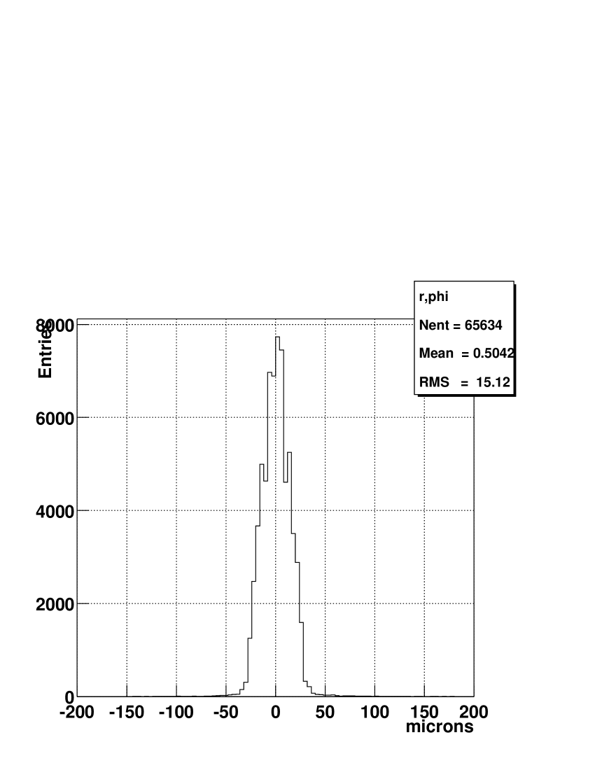
The most important characteristics of the SSD are spatial resolution and detection efficiency. The first is driven by the pitch, the diffusion of the charge cloud in the the wafer bulk, the signal to noise ratios and alignment accuracy. The efficiency is determined by the fraction of dead strips on the detector and dead channels on the ALICE 128C chips, the performance of the connection between the detector and the front end electronics and signal-to-noise ratios. Prototypes of the detection modules, as well as of the Control and ADC boards were tested off-line and in-beam at CERN. Figure 6 shows typical histograms of signal-to-noise ratios obtained from in-beam tests. The 2-D spatial resolution was estimated from the beam-test data by reconstructing impact points on both sides of detectors and combining these information. The values are around 15 m in the direction ( figure 7)and 750 m in the direction along the strips (corresponding to the beam axis in STAR)[11]. These spatial resolutions are driven by the intrinsic resolution on each side, which are typically of 20 m and the stereo angle. Due to the quality of the selected detectors, chips and to the TAB connection, one can expect a level of dead channels below in average. This quality is achived through full tests of all the components at all stages of the production and assembly phases : detector, chip, hybrid, module, ladder, clamshell. All information collected during these tests is stored in a database111wwwstar-sbg.in2p3.fr which may be accessed at any time and from anywhere[13]. This database system provides information for monitoring the production, selecting elements for the assembly and eventually checking the status of the whole detector.
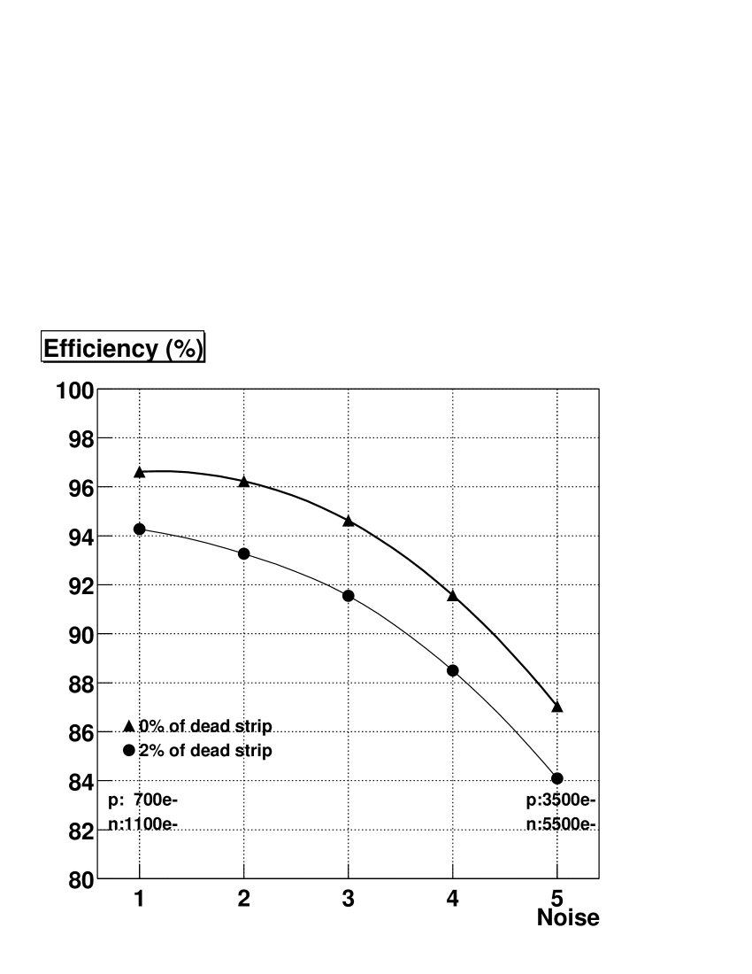
A detailed simulation of the detector as well as a hit reconstruction algorithm have been developped to evaluate the global performances of the SSD [6]. The method uses the matching of the signal amplitudes on both side of the detector for the same particle to solve ambiguous situation where several particle hits are close together. In nominal conditions for the noise and the number of dead channels the hit reconstruction reaches 95 % efficiency with 98 % purity. The dependence of the efficiency on the noise level and the number of dead strips is pictured in figure 8. The general trend is that the efficiency decreases steadily with the average number of dead strips whereas it is much more stable with respect to the noise. The purity is less sensitive to this condition and stays above even for dead strips or 4 times nominal noise level.
7 Summary
The Silicon Strip Detector for STAR with around 1 m2 of sensitive surface and half a million channels is one of the largest one-layer system using the doubled sided silicon strip technology, see summary table 1. A compact module design was achieved by using a novel Tape Automated Bonding method to connect both sides of the silicon wafers to the front end electronics. Other innovative solutions were used like air flow cooling and full remote control of the front-end electronics to minimize the material budget and to handle the large amount of parameters needed to operate the SSD.
Position resolutions of m in the transverse to beam direction and m in the beam direction were measured with beam test. A full simulation with realistic noise and dead channel conditions was performed and yelded a 95 % efficiency with 98 % purity for hit reconstruction.
The detector is currently in production phase and will be installed in STAR in 2002. Exhaustive testing of all the sensitive pieces are conducted and results are stored in a database for further use during the operation of the detector.
| General layout | |
|---|---|
| radius | 230 mm |
| ladder length | 1060 mm |
| acceptance | |
| of ladders | 20 |
| of wafers per ladder | 16 |
| total of wafers | 320 |
| Silicon wafers characteristics | |
| of sides per wafer | 2 |
| of strips per side | 768 |
| total readout channels | 491520 |
| silicon wafer sensitive area | 73 x 40 mm |
| total silicon surface | 0.98 m2 |
| wafer pitch | 95 m |
| resolution | |
| z resolution | |
| operating voltage | V |
| leakage current for one wafer | |
| Readout front-end electronics | |
| of input channels per circuits | 128 |
| total of circuits | 3840 |
| dynamical range | MIPs |
| shaping time | |
| Signal / Noise | |
| SSD total readout time | 5 ms |
| Expected performances | |
| dead channels level | |
| hit reconstruction efficiency | |
| hit reconstruction purity | |
References
- [1] STAR SSD Collaboration, Proposal for a silicon strip detector for STAR, STAR note SN-0400
- [2] S. Bouvier, TAB : a packaging technology used for silicon strip detector to front end electronics interconnection, Proceedings of the workshop on electronics for LHC experiments, Rome, Sept. 1998.
- [3] J.R. Lutz et al., Detector and front-end electronics for ALICE and STAR silicon strip layers, Proceedings of the workshop on electronics for LHC experiments, Rome, Sept. 1998
- [4] ALICE Collaboration, Technical Proposal, CERN/LHCC/95-71.
- [5] S. Giliberto et al., Performances of double-sided silicon strip detectors in a high multiplicity environment of the ALICE experiment at LHC., ALICE note INT-99-53
- [6] B. Hyppolyte et al., Silicon strip detector reconstruction chain for the STAR experiment, STAR note SN-0427
-
[7]
M. Germain et al., Irradiation of a silicon-strip detector and readout chips for the ALICE experiment at LHC, NIM A434 (1999) 345-357
M. Germain et al., Irradiation of silicon-strip detector for the ALICE experiment at LHC, ALICE note INT-01-02 - [8] L. Hebrard et al., ALICE 128C : a CMOS full custom ASIC for the readout of silicon strip detectors in the ALICE experiment, proceeding of the workshop on electronics for LHC experiments, London, Sept. 1997
- [9] D. Bonnet et al., Control System of the silicon microstrip layer of the STAR experiment, Proceedings of the ICALEPS’99 conference, Trieste, Oct. 99
- [10] J.R. Lutz et al., Production tests of microstrip detector and electronic front-end modules for the STAR and ALICE trackers, Proceedings of the workshop on electronics for LHC experiments, Krakow, Sept. 2000
-
[11]
L. Arnold et al., Beam-test of double-sided silicon strip detector, ALICE note INT-98-05
C. Suire et al., Off and In-beam tests of silicon strip detectors for the ALICE experiment at LHC, ALICE note INT-99-22
F. Retiere et al., Performances of double-sided silicon strip for the ALICE experiment at LHC, ALICE note INT-99-36 - [12] C. Suire et al., TAB connection for the silicon strip detector in STAR, STAR note SN-0431
- [13] J. Baudot, M. Janik, W. Peryt, P. Szarwas et al., A database system for the production of the silicon strip detector for STAR, Proceedings of the International Conference on Accelerator and Large Experimental Physics Control Systems, San Jose, 27-30 November