An algorithm for calculating the Lorentz angle in silicon detectors
Abstract
Future experiments will use silicon sensors in the harsh radiation environment of the LHC (Large Hadron Collider) and high magnetic fields. The drift direction of the charge carriers is affected by the Lorentz force due to the high magnetic field. Also the resulting radiation damage changes the properties of the drift.
In this paper measurements of the Lorentz angle of electrons and holes before and after irradiation are reviewed and compared with a simple algorithm to compute the Lorentz angle.
keywords:
silicon, sensors, detectors, Lorentz angle, magnetic field, CMS1 Introduction
The Lorentz angle , by which charge carriers are deflected in a magnetic field perpendicular to the electric field, is defined by:
| (1) |
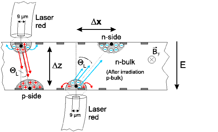
where corresponds to the drift distance along the electric field and to the shift of the signal position (see Fig. 1). If the ionization is produced at the surface, the drift distance equals the detector thickness. If the ionization is produced homogeneously by a traversing particle, the averaged drift distance is only half the detector thickness. The drift mobility in a magnetic field, called the Hall mobility, is denoted by , the drift mobility without magnetic field by . They are related by the Hall scattering factor . This factor describes the mean free time between carrier collisions, which depends on the carrier energy smith . The Hall scattering factor has a value of 0.7 for holes and 1.15 for electrons at room temperature lb . An important question is the dependence of the Lorentz shift on the irradiation dose. Radiation damage can change the drift properties, which will change the Lorentz shift. Such a shift appears as a misalignment of the detector as function of radiation dose, which itself is a function of the distance from the interaction point.
2 Experimental results
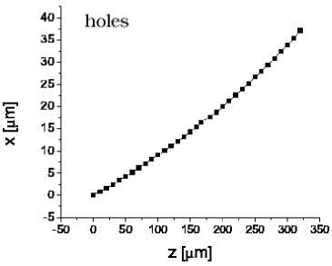
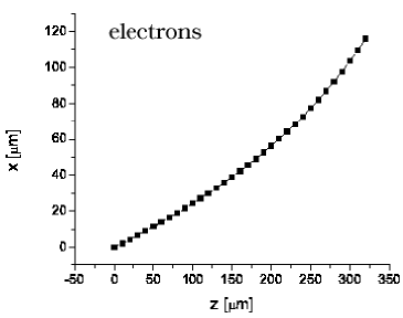
A comprehensive study of Lorentz shifts of non-irradiated and irradiated sensors was performed at Karlsruhe osaka:2000 ; roederer:1998 ; heising:1999 ; hauler:2000 . The Lorentz angle has been measured for electrons and holes separately. A temperature range of 77 K-300 K was covered. The Lorentz angle is measured by injecting charges at the surface on one side and observing the drift through the sensor by measuring the position of the charge on the opposite side (see Fig. 1). Alternative methods are described in Belau:1983 ; Aleppo:2000 .
Charges are generated by injecting laser light with a wavelength of 650 nm, which has an absorption length of 3 m at 300 K. In this case charge carriers of one type are collected at the nearest electrode, whereas the carriers of the other type drift towards the opposite side. This allows the measurement of the Lorentz angle for electrons and holes separately by injecting laser light either on the p- or n-side. The laser from Fermions Lasertech fermions has a maximum power of 1 mW, which could be adjusted by the pulse height and width of the input pulse to the laserdiode. Typically a laser pulse with a width around 1 ns was generated.The laser pulse was sent to the sensor via a single-mode fibre with an inner diameter of a few microns. So the beam spot on the detector could be varied from a few micron onwards by changing the distance between fibre and sensor.
For the measurements the JUMBO magnet from the Forschungszentrum Karlsruhe jumbo has been used in a 10 T configuration with a warm bore of 72 mm. The sensors are double sided microstrip detectors of approximately 2x1 cm from the HERA-B production by Sintef Abt . They have a strip pitch of 50 m on the p–side and 80 m on the n–side; the strips on opposite sides are oriented at an angle of 90∘ with respect to each other. The capacitively coupled read out strips are connected through a 1 M resistor to the bias ring. The read out chip for the strip detectors is the Premux128-Chip with a shaping time of 45 ns jones . The chip’s common mode is suppressed by a double correlated sampling technique, which substracts the signal’s baseline. The threshold could be adjusted but the signal to noise ratio from the laser pulse, corresponding to a few times the signal from a minimum ionizing particle (MIP), was sufficiently high, so that the thresholds were not critical.
The averaged signal position is computed from either a fit with the sum of two Gaussians or from the center of gravity of the pulse heights on neighbouring strips , i.e. . Both methods gave comparable results. The first method was used.
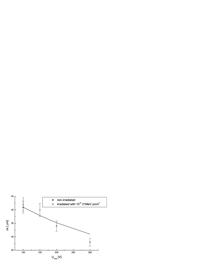
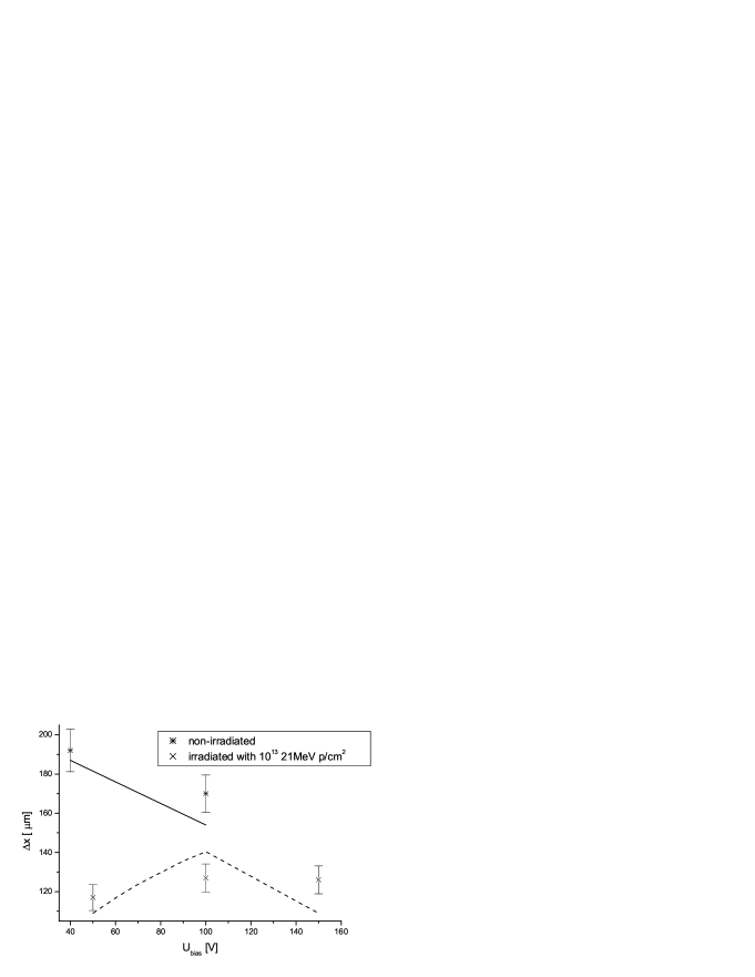
Our measurements showed that the Lorentz shift with the magnetic field are linear up to 9 T osaka:2000 , which means that Eq. 1 can be used. Before irradiation the sensor depletes fully at a bias voltage of 40 V, while after irradiation with 1.01013 21 MeV protons / the depletion voltage increased to 100 V. This implies that the bulk is inverted from n-type to p-type material, as expected rd48 . The bulk damage from 21 MeV protons is about 2.1 times the damage from 1 MeV neutrons huhtinen . Numerical results on the Lorentz angles and shifts are displayed in Figs. 2 and 3 before and after irradiation, respectively.
The Lorentz shift for holes is not strongly depending on irradiation as shown in Fig. 2, while for electrons there is a clear dependence on the irradiation dose as shown in Fig. 3. The calculated values in the Figures are discussed in the next section. The strong decrease of the Lorentz shift for electrons after irradiation for bias voltages below 100 V originates from the fact that the detector is not depleted anymore for these voltages, thus the Lorentz angle is only computed in the depleted zone as will be discussed in section 4.
3 Algorithm for the Lorentz angle at full depletion
At moderate irradiation doses detectors usually can be operated at full depletion. However, for pixel detectors close to the LHC beampipe, this is not necessarily the case. We first discuss an algorithm to calculate the Lorentz angle at full depletion, while the case without full depletion will be discussed in Sect. 4. In this section we first discuss non-irradiated sensors and then the changes needed for moderately irradiated sensors which still can be fully depleted.
3.1 Non-irradiated sensors
The mobility is proportional to the mobility at low electric field . It decreases with increasing electric field until it saturates. It can be parametrized as canali:1975 :
| (2) |
For holes the parameter values used are: while for electrons the following values are used:
The electric field depends on the z-position, the bias voltage, the full depletion voltage and the thickness of the depleted zone of the sensor d:
| (3) |
This equation is an approximation for highly segmented detectors because of the perturbation of the field near the highly doped collection zones of a thickness of a few m. These zones are only a few percent of typical sensor thickness of 300 or 500 m. The averaged electric field can be calculated from Eq. 3 to be:
| (4) |
This Emean is independent of the depletion voltage. The electric field is not constant in a sensor. For full depletion it varies from to zero. For large values of Udepl the electric field can change from the saturation regime to zero with a correspondingly strong change in the mobility.
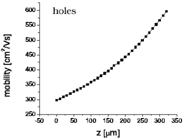
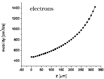
Given the electric field, one can calculate the mobility from Eq. 2.. The total Lorentz shift can be otained by integrating Eq. 1 over the thickness of the sensor using at each position the mobility given by equation 2. For small depletion voltages the use of an averaged electric field and corresponding mobility is enough to calculate the Lorentz shift from Eq. 1. Figs. 2 and 3 show that the calculations match the measurements quite well. The figures also show that the Lorentz shifts vary practically linear with the bias voltage for fully depleted sensors.
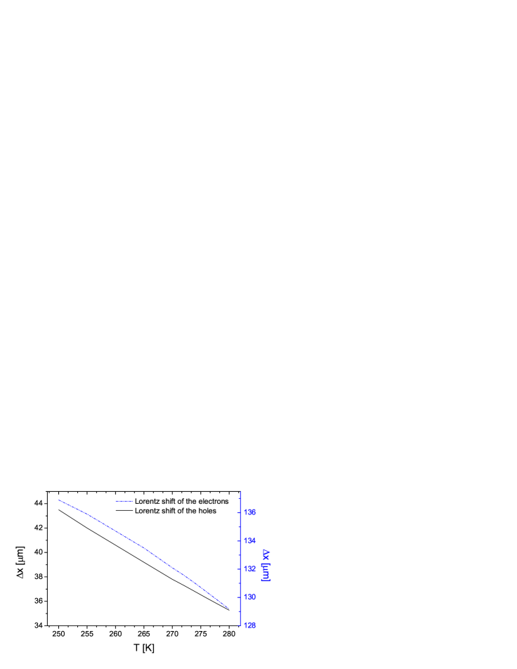
The temperature dependence of the Lorentz shift is shown in Fig. 4. The Lorentz shift varies about 8 m for a 300 m thick sensor at 100 V in a 4 T magnetic field, if the temperature is varied between 250 K and 280 K, for both electrons and holes.
3.2 Irradiated sensors
There are three main parameters, which change after irradiation: the mobility, the electric field and the depletion voltage.
The dependence of the mobility on the irradiation dose is still controversial. In Ref.ere:1995 no significant changes were observed in the transport properties of both electrons and holes up to 0.510 1 MeV n/cm2 and a prediction is made that a fluence of at least about 1015 1 MeV n/cm2 is necessary to affect carrier drift mobilities significantly. In Ref. brod:1999 the mobility for both carrier types in irradiated sensors agree with those for the non-irradiated sensor within errors for fluences up to 21014 1 MeV n/cm2. In contrast a change of mobility after irradiation for holes and electrons was observed in Ref. leroy:1999 :
-
•
The mobility of holes changes slightly from 470 cm2/Vs to about 460 cm2/Vs after irradiation to a fluence of 1013 1 MeV n/cm2. Above this fluence the mobility does not change any more. The change of mobility corresponds to a change in the Lorentz shift of a few percent.
-
•
The mobility of the electrons changes more significantly from 1417 cm2/Vs to 1000 cm2/Vs. The reduction of the mobility is so strong that one has to take this into account when computing the Lorentz shift.
In addition, the Hall scattering factor may change after irradiation. This is equivalent to a change in drift velocity, for what concerns the Lorentz shift. Therefore we keep constant and fit our data with a variable mobility, which can describe the data well, as shown in Table 1. The needed shift in mobility is within the range given in Ref. leroy:1999 . Here we used Eq. 4 to calculate the electric field, since the depletion voltages were reasonably low. For higher depletion voltages the bias voltage is so high, that the saturation of the drift velocity has to be taken into account, which implies the use to Eq. 3 instead of Eq. 4. In this case the depletion voltage has to be known. For electrons the nonlinear saturation regime is reached at lower fields than for holes, because of the higher ratio in Eq. 2. This difference in nonlinearity between electrons and holes is displayed in Fig. 5 for a sensor with a large depletion voltage of 280 V.
| in ∘ | in ∘ | |||
|---|---|---|---|---|
| in V | in m | in ∘ | = 1417 cm2/Vs | = 1100 cm2/Vs |
| at 300 K | at 300 K | |||
| 50 | 117 7 | 21 1 | 24 | 20 |
| 100 | 127 7 | 23 1 | 29 | 25 |
| 150 | 126 7 | 23 1 | 25 | 22 |
In our model we also neglected the effect of double junctions after irradiation and the effect of defects (beattie:1998 -Eremin:2002 ). The justification lies only in the agreement between the model and available data with still rather limited precision.
4 Algorithm for the Lorentz angle at high irradiation doses
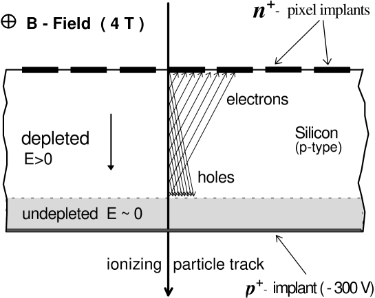
Pixel detectors are located near the beam pipe and therefore have to stand higher radiation doses than strip detectors. It is not guaranteed that they can be always fully depleted. Since the bulk inverts after strong irradiation from n-type to p-type, the pn-junction will be on the n-side and the depletion starts from the n-side. If not fully depleted, there will be a region without electric field, in which only diffusion takes place, as indicated in Fig. 6. This region will not contribute significantly to the signal, so one can consider this sensor as having a sensitive thickness corresponding to the depleted zone. We assume in our algorithm that the Lorentz shift is determined by the sensitive thickness, thus ignoring the undepleted zone. Our algorithm is compared with measurements for the ATLAS pixel sensor reported in Ref. Aleppo:2000 . The charge carriers were generated with a pion beam of 180 GeV/c. The Lorentz angle was determined by measuring the minimum mean cluster size as a function of angle of the incident beam particles. The ATLAS pixel sensors are 280 m thick and have a full depletion voltage before irradiation of about 150 V. The magnetic field during the measurements was 1.4 T and the temperature 300 K for the non-irradiated sensors and 263 K for the irradiated sensors. The measured values are compared to the simulated values in Table 2.
| Fluence | Depl. depth | in ∘ | in ∘ | ||
| n/cm2 | in V | in m | in ∘ | = 1417 cm2/Vs | = 1100 cm2/Vs |
| at 300 K | at 300 K | ||||
| 0 | 150 | 283 6 | 9.0 0.9 | 8.4 | |
| 51014 | 150 | 123 19 | 5.9 1.3 | 6.7 | 5.7 |
| 51014 | 600 | 261 8 | 2.6 0.5 | 4.4 | 3.9 |
| 1015 | 600 | 189 12 | 3.1 1.0 | 3.8 | 3.5 |
| 1015 | 600 | 217 13 | 2.7 0.8 | 3.2 | 3.0 |
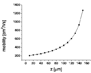
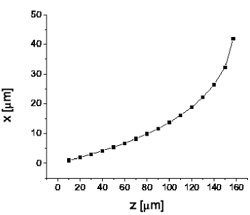
In the simulation the strong irradiation is taken into account by replacing the total sensor thickness in Eq. 3 by the depleted thickness, which is determined by the maximum possible bias voltage. The high bias voltage leads to a strongly varying mobility in a not fully depleted sensor, as shown in Fig. 7. The trajectory of the drifting ionization is correspondingly non-linear, so the integration of the Lorentz shifts has to be done in sufficiently small steps. The Lorentz angle, given in Table 2, is defined as the arc tangent of the total Lorentz shift divided by the depleted sensor thickness. Comparing the simulations with the measurements one observes that the data can be fitted better with lower mobilities after irradiation, as expected from the discussion in Sect.3.2. So it has been shown that the proposed algorithm also works for n-side readout of not fully depleted sensors after strong radiation, i.e. pixel detectors, if the reduced sensitive thickness is taken into account.
5 Summary
The Lorentz angle is determined by electric and magnetic fields and can be modelled by Eqs. 1, 2 and 3 or 4. Because of the different mobility and Hall scattering factor for holes and electrons, the Lorentz shift for electrons is at least four times the one for holes. Irradiation decreases the electron mobility at low electric fields significantly. The hole mobility is hardly affected by irradiation.
The simulated data have been compared with measured values from HERA-B test structures and the ATLAS pixel sensor. It has been shown that the algorithms developed here simulate the Lorentz shifts reasonably well, if one takes into account the reduced electron mobility after irradiation.
References
- (1) R.A. Smith, Semiconductors, Cambridge Univ. Press, 1968.
- (2) Landolt-Börnstein, Numerical Data and Functional Relationships in Science and Technology, Group III, Vol. 17a, Springer Verlag, Berlin, 1982.
- (3) C.Canali et al., Electron and hole drift velocity measurements in silicon and their empirical relation to electric field and temperature, IEEE Trans. on Electron Devices, Vol.ED-22, 1045–47, 1975.
- (4) G. Masetti et al., Modelling of carrier mobility against carrier concentration in Arsenic-, Phosphorus- and Boron-doped silicon, IEEE Trans. on Electron Devices, Vol.ED-30, 764–69, 1983.
- (5) N.D. Arora et al., Electron and hole mobilities in silicon as a function of concentration and temperature, IEEE Trans. on Electron Devices, Vol.ED-29, 292–295, 1982.
- (6) W. de Boer et al., Lorentz angle measurements in irradiated silicon detectors between 77K and 300K, Nucl. Instr. and Meth. A 461 (2001), 200–203; Nucl. Instr. and Meth. A 478 (2002), 330-332;
- (7) F. Röderer, Messung von Lorentz-Winkeln in Silizium-Detektoren, Diplomarbeit, Univ. of Karlsruhe, IEKP–KA/98–24 (in german only).
- (8) S. Heising, Silicon detectors for high energy physics experiments at low temperatures and high magnetic fields, Ph. D. thesis. Univ. of Karlsruhe, IEKP–KA/99–26 (in german only).
- (9) F. Hauler, Lorentzwinkelmessungen an bestrahlten Silizium-Streifendetektoren im Temperaturbereich T=77-300K, Diplomarbeit, Univ. of Karlsruhe, IEKP–KA/2000–12 (in german only).
- (10) E. Belau et al., Charge Collection in Silicon Strip Detectors, Nucl. Instr. and Meth. A 214 (1983) 253.
- (11) M. Aleppo, A measurement of Lorentz angle of radiation-hard pixel sensors, Nucl. Instr. and Meth. A 465(2001), 108–111.
- (12) http://www.fermions.com
- (13) F. Hornung, A. Rimikes, Th. Schneider, High Magnetic Field facilities and Projects at the Forschungszentrum Karlsruhe, Internal Note, 1999.
- (14) I. Abt et al., Cluster shapes and cluster sizes in the HERA-B silicon vertex detector, Nucl. Instr. and Meth. A 469(2001), 147–158
- (15) L.L. Jones, PreMux128 Specification version 2.3, Rutherford Internal Note, 1995.
- (16) RD48 collaboration, http://rd48.web.cern.ch, ROSE/TN/2000-03, Nucl. Instr. and Meth. A 466 (2001) 308.
- (17) M. Huhtinen, Simulation of non-ionising energy loss and defect formation in silicon, RD48 Technical Note 2001-02, Cern(2001), submitted to Nucl. Instr. and Meth. B.
- (18) CERN/LHCC 98-6(1998), The CMS Collaboration, The Tracker Project Technical Design Report.
- (19) CERN/LHCC 2000-16(2000), The CMS Collaboration, Addendum to the CMS Tracker TDR.
- (20) E. Focardi et al., The CMS silicon tracker, Nucl. Instr. and Meth. A 453(2000), 121.
- (21) Pixel CMSIN1998/3, R. Kaufmann and B. Henrich, Charge Drift in Silicon, 1998.
- (22) V. Eremin et al., Carrier drift mobility study in neutron irradiated high purity silicon, Nucl. Instr. and Meth. A 362(1995), 338–343.
- (23) T.J. Brodbeck et al., Carrier Mobilities in Irradiated Silicon, ROSE/TN/2000-09.
- (24) C. Leroy et al., Charge transport in non-irradiated and irradiated silicon detectors, Nucl. Instr. and Meth. A426(1999), 90–102.
- (25) L.J. Beattie et al., The electric field in irradiated silicon detectors, Nucl. Instr. and Meth. A 418(1998), 314–321.
- (26) G. Casse et al., Study of evolution of active volume in irradiated silicon detectors, Nucl. Instr. and Meth. A426(1999), 140–146.
- (27) D. Menichelli et al., Modelling of the observed double-junction effect, Nucl. Instr. and Meth. A 426(1999), 135–139.
- (28) V. Eremin et al., Effect of radiation induced deep level traps on Si detector performance, Nucl. Instr. and Meth. A 476(2002), 537–549.
- (29) RD39 Collaboration, Nucl. Instr. and Meth. A 440 (2000) 5-16 and http://rd39.web.cern.ch, RD39 Status Report CERN/LHCC 2000-010, 06-Jan-2000.