Polarization state of the optical near–field
Abstract
The polarization state of the optical electromagnetic field lying several nanometers above complex dielectric–air interfaces reveals the intricate light–matter interaction that occurs in the near–field zone.From the experimental point of view, access to this information is not direct and can only be extracted from an analysis of the polarization state of the detected light. These polarization states can be calculated by different numerical methods well–suited to near–field optics. In this paper, we apply two different techniques (Localized Green Function Method and Differential Theory of Gratings) to separate each polarisation component associated with both electric and magnetic optical near–fields produced by nanometer sized objects. A simple dipolar model is used to achieve insight into the physical origin of the near–field polarization state. In a second stage, accurate numerical simulations of field maps complete data produced by analytical models. We conclude this study by demonstrating the role played by the near–field polarization in the formation of the local density of states.
pacs:
42.79.G, 42.82.E, 07.79.FI Introduction
Light interactions with dielectric or metallic surfaces displaying well–defined subwavelength–sized structures (natural or lithographically designed) give rise to unusual optical effectsPohl-Courjon:1993 ; Reddick-Warmack-Ferrell:1989 ; Fischer-Pohl:1989 ; Dawson-deFornel-Goudonnet:1994 ; Goudonnet-Bourillot-Adam-DeFornel-Salomon-Vincent:1995 ; Krenn:1995 ; Krenn-Weeber-Dereux-Bourillot-Goudonnet-Schider-Leitner-Aussenegg-Girard:1999 ; Weeber-Bourillot-Dereux-Chen-Goudonnet-Girard:1996 ; Weeber-Girard-Dereux-Krenn-Goudonnet:1999 ; Weeber-Dereux-Girard-Krenn-Goudonnet:1999 ; Weeber-Dereux-Girard-Colas-Krenn-Goudonnet:2000 ; Girard-Joachim-Gauthier:2000 . The recently observed “light confinement state” in which the light field is trapped by individual surface defects, belongs to this class of phenomenaWeeber-Bourillot-Dereux-Chen-Goudonnet-Girard:1996 . Although, with usual dielectric materials (silica for example), the local near–field intensity variations observed around the particles (or structures) remains moderate over the optical spectrum (between 10 to 40 per cent of the incident light intensity), these variations can nevertheless be easily mapped with the tip of a Photon Scanning Tunneling Microscope (PSTM)Weeber-Bourillot-Dereux-Chen-Goudonnet-Girard:1996 . The images recorded with this technique reveal dramatic changes when passing from the TM (transverse magnetic) to the TE (transverse electric) –polarized modes. In general, TM–polarized light tends to display larger contrast than TE–polarized light. ¿From the experimental point of view, the definition of the polarization direction of the incident and detected intensity must be defined with respect to a unique incident plane. About six years ago Van Hulst and collaborators proposed a clever probe configuration devoted to polarization mapping Propstra-VanHulst:1995 . These authors performed these measurements by using a combined PSTM/AFM microscope in which detection is implemented by a microfabricated silicon–nitride probe. ¿From this technique, polarization contrast is extracted by changing the polarization directions of both the incident and the detected light. The main findings gathered in this workPropstra-VanHulst:1995 , concern the relative efficiency of the four excitation–detection possibilities (TE/TE,TE/TM,TM/TE,and TM/TM) to record a highly resolved PSTM image. In particular, the efficiency of the TM/TM acquisition mode is well reproduced. Although a complete interpretation of this work requires a realistic numerical implementation of the combined AFM/PSTM probe tip, we can obtain useful information by analyzing the near–field polarization state versus the polarization state of the illumination mode.
In addition, in closely related contexts, the control of the near–field polarization state provides an interesting and versatile tool for generating powerful applications (tunneling time measurements Balcou-Dutriaux:1997 , highly–resolved microscopy and spectroscopy Pohl-Courjon:1993 , surface plasmon resonance spectroscopy of molecular adlayers Jung-Campbell-Chinowsky-Mar-Yee:1998 , atom optics Landragin-Courtois-Labeyrie-Vansteenkiste-Westbrook-Aspect:1996 ; Esslinger-Weidemuller-Hemmerich-Hansch:1993 . More precisely, in the field of atom optics and interferometry, one is interested in building diffraction gratings that can play the role of beam splitters. Several devices have been successfully realised, ranging from mechanical transmission gratings to light standing waves in free space or evanescent for a prism. For a general review the reader is referred to interfero . To circumvent some theoritical limitations CHenkel it has been recently proposed Balykin to use micrometer sized metallic stripes to shape the evanescent field. A full near-field, metallic/dielectric approach open obviously new perspectives. In particular the spacing period is no longer linked to the atomic optical transition and a reflection stucture cannot clug. More, higher harmonics in the optical evanescent field can be tuned to produce for example a blazed atomic grating. Nevertheless, the optical potential is strongly related to the light field polarisation, which is a farther motivation for the present study. We will begin our theoretical analysis with a simple dipolar scheme in which the main experimental parameters (incident angle, optical index, polarization of the incident light, …) appear explicitlyGirard-Courjon:1990 ; Keller-Xiao-Bozhevolnyi:1992 ; Keller:1996 . In a second stage, these results will be completed with an ab–initio approach allowing objects of arbitrary shape to be treated exactly.
II Polarization of the light above a single dielectric particle
To illustrate the coupling between a polarized incident wave and a small spherical object lying on the sample, we consider the simple dipolar model depicted in Fig. 1.
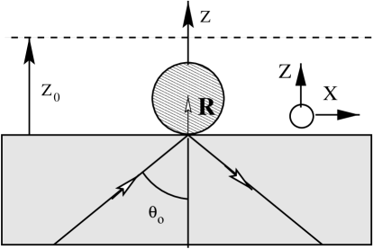
The substrate modifies the polarizability of the particle. We have then
| (1) |
with
| (2) |
where is the nonretarded propagator associated with the bare surface, and labels the particle location. Within this description, the optical properties of the spherical particle–surface supersystem is described in terms of a “dressed” polarizabilityGirard-Dereux-Weeber:1998 ; Keller:1996 . The analytical form of can be derived from Eq. (10) of reference 5. This dyadic tensor remains diagonal with two independent components (perpendicular to the interface) and (parallel to the interface):
| (3) |
and
| (4) |
where is the optical index of refraction of the substrate.
II.1 New field components in the near–field domain
At an observation point located above the sample ( 0) and in the immediate proximity of the particle, the incident light field is locally distorted. As illustrated in Ref. Martin-Girard-Dereux:1995:2 , these distortions generate not only a profound modification of the intensity level (both electric and magnetic), but also a complete change of the polarization state. At subwavelength distances from the scatterers, we expect therefore to observe the occurrence of new components that were absent in the incident field . The physical origin of this polarization transfer can be easily understood if we introduce the two relevant field propagators and that establish the physical link between the oscillating dipole = and the new near–field state generated above the particle
| (5) |
and
| (6) |
where in the near–field zone, i.e. when ,
| (7) |
and
| (11) |
The discussion of the two equations (5) and (6) can be made easier when considering specific examples.
II.2 Illumination with a TE–polarized surface wave
In this incident polarization mode, the electric field is directed along the (OY) axis. We have then = . Let us see what happens when the observation point moves along the diagonal straigth line (A–B) schematized in figure 2.
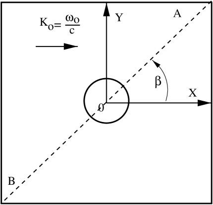
For a given angle, the introduction of the position vector = (where varies between and ) along the line (A–B), allows the electric field polarization evolution to be observed when passing over the particle. Each cartesian component can be simply extracted from Eq. (5). This leads to three analytical relations:
| (12) |
| (13) |
with
| (14) |
and
| (15) |
Some interesting features can be deduced from these equations. (i) First, we observe that the polarisation is not modified when the observation point is perpendicular the particle center (i.e. when r = 0). The set of equations reduces then to
| (16) |
| (17) |
and
| (18) |
Clearly the effective polarizability reduces the electric field magnitude compared to its initial value. This fact explains the observation of contrasted dark zones above small particles lighted with the TE polarization (c.f. Fig. (4)). (ii) Around the particle (when R/2 r 2R) two new components, namely and , define a new local polarization state. These components vanish again when the observation point moves away from the particle. Similar relations can be derived for the TM–polarized mode from Eq. (5).
To conclude this section, let us examine what happens with the magnetic field part (cf. Eq. 6). Since in the reference system of Fig. (1), the incident magnetic field displays two components different from zero, = , we can write
| (19) |
| (20) |
and
| (21) |
Unlike what happens with the electric field, the particle does not produce new magnetic field components in the near-field. In this case, the polarization change corresponds to a different balance in the initial components. It is important to recall that we have used the dipole approximation to describe the particle-field interaction, i.e. the size of the particle is assumed to be small compared to the wavelength of light. In a more realistic calculation, with nanostructures of characteristic dimension 100 nanometers this result is not rigorously exact. However, we still expect, in TE polarization mode, a negligible particle contribution to compared to the total magnetic field intensity.
III AB INITIO study of the near–field polarization state
Analytical results presented in the previous section supply qualitative information about the spatial polarization state distribution. In a recent paper, analysis of polarization effects was proposed in the context of near–field optics in which a limited number of single particles were investigatedRichard:2001 . Since in many practical situations experimentalists are interested in lithographically designed structures, these preliminary analyses must be completed by ab initio procedures for solving Maxwell’s equations.
III.1 Localized objects
Recently, theoretical modelling in the vicinity of localized objects was performed in the framework of the field susceptibility methodGirard-Bouju-Dereux:1993 ; Greffet-Carminati:1997 . Today, this method is one of the most versatile and reliable numerical techniques to solve the full set of Maxwell equations for the typical parameters of near–field optics. It works well even for metallic nanostructures (see for example referencesKrenn-Weeber-Dereux-Bourillot-Goudonnet-Schider-Leitner-Aussenegg-Girard:1999 ; Weeber-Girard-Dereux-Krenn-Goudonnet:1999 ; Weeber-Dereux-Girard-Krenn-Goudonnet:1999 ). This approach (called the Direct Space Integral Equation Method (DSIEM)) is based on the knowledge of the retarded dyadic tensor associated with a reference system which, in our problem, is a flat silica surfaceMartin-Piller:1998 ; Martin-Girard-Smith-Schultz:1999 . The numerical procedure considers any object deposited on the surface as a localized perturbation which is discretized in direct space over a predefined volume mesh of N points . In a first step, the electric field distribution is determined self-consistently inside the perturbations (i.e., the source field). At this stage, a renormalization procedure associated to the depolarization effect is applied to take care of the self-interaction of each discretization cell. The final step relies on the Huygens–Fresnel principle to compute the electromagnetic field on the basis of the knowledge of the field inside the localized perturbations . The two main computational steps can be summarized as follows:
(i) Local field computation inside the source field
| (22) |
where labels the generalized field propagator of the entire system (localized object plus bare silica surface). In the representation it is given by
| (23) |
where represents the electric susceptibility of the localized object, is the volume of the elementary discretization cell, and is the field–susceptibility of the entire system. This last quantity is usually computed by solving Dyson’s equation:
| (24) | |||
(ii) Electric and magnetic near–field mapping computation around the source field region
| (25) | |||
and
| (26) | |||
In the numerical work to be discussed in this section, the retarded propagators and have been chosen in referenceGirard-Weeber-Dereux-Martin-Goudonnet:1997 .
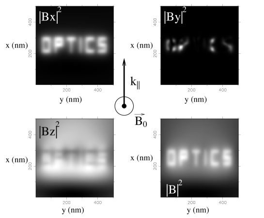
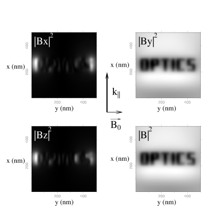
The test–object we consider in this section is the word OPTICS engraved at the surface of a layer deposited on a silica surface.

Intentionally we have chosen a planar structure devoid of any symmetry. In order to gain more insight in the polarization changes occurring around such complex lithographically designed nanostructures, we analyze in Figs. (4)-(7) the electric and magnetic near–field intensities generated by each cartesian component (, , ) and (, , ). For comparison, the square modulii are also provided.
III.1.1 Dielectric materials
The lateral dimensions of the object are given in Fig. (3). The thickness and the optical index of the pattern is 20 nm and 2.1, respectively. The wavelength of the incident laser is 633 nm. All fields are computed 10 nm above the surface of the structure, i.e. 30 nm above the glass-air interface.
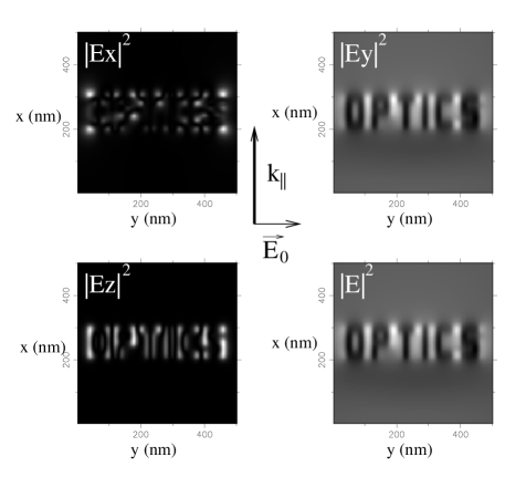
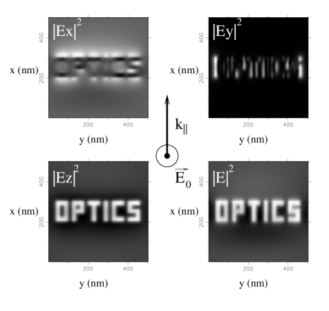
The incident light is a TM/TE–polarized evanescent surface wave traveling along the axis. This illumination condition is used in the Photon Scanning Tunneling Microscope (PSTM). Some general comments can be made about these results. First, all components of both the electric and magnetic fields have been excited in the near-zone. The occurence of these new components is a pure near–field effect because it is always localized around the structures. In Figs. (4) and (5) we display the electric field part. As predicted in section 2, we recover the appearance of two additional components, and , when the object is excited by a TE–polarized surface wave. In agreement with the PSTM results, numerous regions appear with a dark contrast and a moderate intensity level.
As expected, the excellent image–object relation currently observed in the TM–polarized mode is mainly provided by the field component normal to the object. The two other contributions tend to slightly degrade the total pattern composed by the superposition of the three maps , and .
The magnetic near–field intensity maps (cf. Figs. 6, 7) also show a significant confinement of the magnetic field over the particle which reverses the contrast with respect to the electric map. Similarly to what happens with the electric field, the role played by the additional components can degrade the topographic information contained in the complete field maps. Notice in Fig. (6) that, as mentioned in section II, the new y-component of the magnetic field is very small compared to the total magnetic field.
III.1.2 Metallic materials
In the above formalism, the only parameter distinguishing metallic from dielectric objects is the linear susceptibility . Alternative procedures can be adopted to describe the metallic susceptibility. For example, a direct route would consist in expanding the susceptibility in a multipolar series around the geometrical center of the metallic particle. While this scheme allows non–local and quantum size effects to be included, it is nevertheless restricted to simple particle shapes (spheres, ell0ipsoids, etc.). When dealing with spherical metallic clusters having a typical radius below 15 nm this description is mandatory and can be easily included in the DSIEM formalismGirard:1992 . For the applications discussed in this paper, involving lithographically designed metallic structures larger than this critical size, we can adopt the discretization of over all the volume occupied by the particle. In this case, the local susceptibility is just related to the metal optical index by the relationWeeber-Girard-Dereux-Krenn-Goudonnet:1999 :
| (27) |
In the visible range, the numerical data for describing both real and imaginary parts of have been tabulated by PalikPalik:1985 for different metals.
We present in Fig. (8) a gray scale representation of the electric field distribution computed above the topographical object depicted in Fig. 3. In this case, the high optical metal index generates complex field patterns without clear relation to the topography. Furthermore the possible excitation of localized plasmons reinforces this phenomena and some parts of the localized metal pattern (e.g. the corners) can even behave as an efficient light sources.
III.2 Periodic surface structures
When working with periodic surface structures, the localized Green’s function method described above is no longer applicable. But any figure can be decomposed in points (direct space) or Fourier components ( reciproqual space). We thus can use two methods wether the real object contain few points or few Fourier components. In the case of periodic gratings, the field distribution can be investigated with this second class of methods Petit:1980 ; Maystre-Neviere:1978 ; Montiel-Neviere:1994 . The so–called differential theory of gratings (DTG) was originally developed twenty years ago to predict the efficiencies of one– and two–dimensional diffraction gratings. Based on a rigorous treatment of Maxwell’s equations, this method can also be used efficiently to determine the optical near–field scattered by three dimensional periodic objects. In the following subsection, in order to avoid a complete presentation of this well–established technique, we will only summarize the essential steps of the computational procedure.
As in previous sections, we are interested in the electromagnetic near-field diffracted above objects engraved on an interface illuminated by total internal reflection. When using the DTG methodPetit:1980 , the electromagnetic field above the grating can be expanded in a Fourier series
| (28) |
where = = , represents either the electric field or the magnetic field . The 3D–wave vectors , associated with the harmonic obey the well-known dispersion equation
| (29) |
The set of wave vector parallel to the surface are simply defined for each couple of integer numbers by
| (30) |
where and denote respectively the period of the grating along the 0x– and 0y–directions. From Eq. (29), it may be seen that the coefficient may be either real or purely imaginary. Real values of correspond to radiative harmonics while imaginary values introduce evanescent components in the expansion (28).
In a general way, the six components of the electromagnetic field can be deduced from two independent parameters usually named the principal components. Let us choose, for example, the y–components and as principal components. It is a simple matter to show that the Fourier y–components of the field just above the surface of objects can be expressed as a linear combination of the y–components of the incident field:
| (31) |
The transmission coefficients , , and describe the coupling between the electric and magnetic harmonics composing the scattered and the incident field. These coefficients depend both on the geometry of the sample and on the angular conditions of incidence but not on the polarization of the incident light. The polarization of the incident plane wave is controlled by the values of and . From a numerical point of view, the transmission coefficients are obtained by the inversion of a complex square matrix whose dimension is (where is the total number of harmonics used to describe the scattered field in Eq. (28)). Columns of this matrix contain the Fourier y–components of the electromagnetic field which would have illuminated the periodical objects in order to obtain a pure harmonic field just above the nanostructure. A detailed description of the calculation of the matrix elements can be found in Refs. Petit:1980, ; Montiel-Neviere:1994, . With Eq. (31), we can calculate all the Fourier components of electric and magnetic fields just above the objects, which are used as initial conditions to obtain the field anywhere.
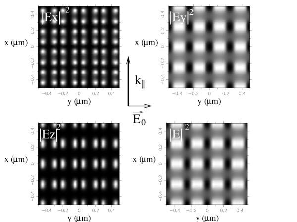
General remarks about contrast, relative intensities and image-object relation have been made previously (see sections II.2 and III.1.1), therefore we only highlight the specific electromagnetic properties of periodic structures.
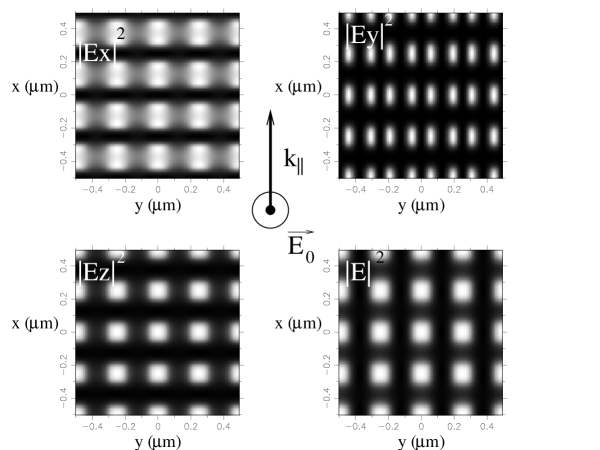
We studied a lattice of nm3 dots, separated by nanometers. A strong localization of the electric field appears above the pads in TM-polarized mode or between the pads in TE-polarized mode. Moreover, a careful analysis of the different components shows that it is possible to create a particular field map such as field lines oriented along y-axis ( in TE-mode) or x-axis ( in TM-mode), or periodic field spots with very different characteristics (spot size, periodicity and shape) considering the other components in the two polarization modes. These particular field components distribution could have a great interest for the interaction of cold atoms with optical evanescent waves Kobayashi-Sangu-Ito-Ohtsu:2000 ; Birkl-Buchkremer-Dumke-Ertmer:2001 .
IV Local density of state and polarization effects
Unlike what happens with electronic surface states, the Local Density of photonic States (the so–called photonic LDOS) contains information related to the polarization of the excitation field. It is well established that the density of states near surfaces plays a significant role in near–field physics Girard-Joachim-Gauthier:2000 . In particular, the photonic LDOS is a useful concept for the interpretation of fluorescence decay rate in the very near–field Barnes:1998 and could help in understanding image formation produced by illuminating–probe SNOM Dereux-Girard-Weeber:2000 . By referring to the electric field, we deduce the optical LDOS from the field–susceptibility of the entire system (plane surface plus supported nanostructures, see section III.1) Agarwal:1975c ; Dereux-Girard-Weeber:2000
| (32) |
In this expression, the optical LDOS is related to the square modulus of the electric field associated with all electromagnetic eigenmodes of angular frequency . Because of the vectorial character of electromagnetic fields, it is very useful to introduce three polarized optical LDOS also called partial LDOS, so that Dereux-Girard-Weeber:2000
| (33) | |||||
| (34) |
The three different polarized optical LDOS computed over a pattern made of three dielectric cylinders of optical index 2.1 are represented on figure 11.
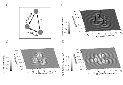
At this stage, we can made some general remark. In the configuration investigated in figure (11) we can verify that both X–LDOS and Y–LDOS are almost identical with just a rotation of between them. Nevertheless, this properties does not subsist any more if we reinforce the optical coupling between the dielectric posts. More precisely, certain arrangements of nanoscale pillars (circular or ellipsoidal) can force light waves into states generated by the collective coupling between the pillars leading to significant difference between X–LDOS and Y–LDOS maps.
Moreover, although optical LDOS characterizes the spectroscopic properties of an electromagnetic system independently of the illumination mode, it is interesting to note the strong analogy between the dark contrast over the pads obtained for Y–LDOS and the dark contrast that appears in the case of s-polarized illumination mode (i-e incident electric field along the y-axis) observed in section II.2. In addition, as in the case of optical near–field maps discussed in the previous section, the polarized LDOS’s can display significant discrepancies relatively to the shapes of the underlying objects.
Finally, let us note that partial LDOS’s are not only a powerful mathematical tool but can easily be linked to the physical properties of electromagnetic systems. The most famous example is the fluorescence lifetime of a molecule near an interface which critically depends on the spatial LDOS variation Wylie-Sipe:1984 ; Girard-Martin-Dereux:1995 ; Metiu:1984
V Conclusion
On the basis of both simple analytical model and sophisticated 3D Maxwell’s equations solvers this paper has focussed on the unusual behaviour of the light polarization in the near–field. When subwavelength patterned objects are excited by a surface wave of well–defined polarization, a complex rotation of the light polarization state can be expected in the near zone. This phenomenon localized around the scatterer is a typical near–field effect. The occurrence of new components is more pronounced in the electric field than in the magnetic part. Subwavelength features are present in all components but with very different energy levels.
References
- (1) in Near-field optics, Vol. E 242 of NATO ASI, NATO, edited by D. Pohl and D. Courjon (Kluwer, Dordrecht, 1993).
- (2) R. C. Reddick, R. J. Warmack, and T. L. Ferrell, Phys. Rev. B 39, 767 (1989).
- (3) U. Fischer and D.W. Pohl, Phys. Rev. Lett. 62, 458 (1989).
- (4) P. Dawson, F. de Fornel, and J. P. Goudonnet, Phys. Rev. Lett. 72, 2927 (1994).
- (5) J. P. Goudonnet et al., J. Opt. Am . Soc. 12, 1749 (1995).
- (6) J. Krenn, in Photons and local probes, Vol. E 300 of NATO ASI, edited by O. Marti (Kluwer, Dordrecht, 1995), 181
- (7) J. Krenn et al., Phys. Rev. B 60, 5029 (1999).
- (8) J. Weeber et al., Phys. Rev. Let. 77, 5332 (1996).
- (9) J. Weeber et al., J. Appl. Phys. 86, 2576 (1999).
- (10) J. Weeber et al., Phys. Rev. B 60, 9061 (1999).
- (11) J. Weeber et al., Phys. Rev. E 62, 7381 (2000).
- (12) C. Girard, C. Joachim, and S. Gauthier, Rep. Prog. Phys. 63, 893 (2000).
- (13) K. Propstra and N. K. V. Hulst, J. of Microscopy 180, 165 (1995).
- (14) P. Balcou and L. Dutriaux, Phys. Rev. Let. 78, 851 (1997).
- (15) L. D. Jung et al., Langmuir 14, 5636 (1998).
- (16) P.R.Berman Ed., Academic Press, Atom Interferometry, London (1997).
- (17) C. Henkel et al, Appl. Phys. B 6̱9, 277 (1999).
- (18) V.I.Balykin et al, Opt. Commun., 145, 322 (1998).
- (19) A. Landragin et al., Phys. Rev. Lett. 77, 1464 (1996).
- (20) T. Esslinger, M. Weidemüller, A. Hemmerich, and T. W. Hänsch, Opt. Let. 18, 450 (1993).
- (21) C. Girard and D. Courjon, Phys. Rev. B 42, 9340 (1990).
- (22) O. Keller, M. Xiao, and S. Bozhevolnyi, Surf. Sci. 280, 217 (1992).
- (23) O. Keller, Physics Reports 268, 85 (1996).
- (24) C. Girard, A. Dereux, and J. C. Weeber, Phys. Rev. E 58, 1081 (1998).
- (25) O. J. F. Martin, C. Girard, and A. Dereux, J. Opt. Soc. Am. A 13, 1801 (1995).
- (26) N. Richard, Phys. Rev. E 63, 26602 (2001).
- (27) C. Girard, X. Bouju, and A. Dereux, in Near-Field Optics, Vol. E 242 of NATO ASI, edited by D. Pohl and D. Courjon (Kluwer, Dordrecht, 1993), pp. 199–208.
- (28) J.-J. Greffet and R. Carminati, Progress in Surface Science 56, 133 (1997).
- (29) N. B. Piller and O. J. F. Martin, IEEE Trans. Antennas Propag. 46, 1126 (1998).
- (30) O. J. F. Martin, C. Girard, D. R. Smith, and S. Schultz, Phys. Rev. Let. 82, 315 (1999).
- (31) C. Girard et al., Phys. Rev. B 55, 16487 (1997).
- (32) C. Girard, Phys. Rev. B 45, 1800 (1992).
- (33) D. Palik, Handbook of Optical Constants of Solids (Academic Press, New York, 1985).
- (34) R. Petit, Electromagnetic theory of gratings (Springer Verlag: Topics in current physics, Heidelberg, 1980), Vol. 22.
- (35) D. Maystre and M. Nevière, J. Opt. 9, 301 (1978).
- (36) F. Montiel and M. Neviere, J. Opt. Soc. Am. A 11, 3241 (1994).
- (37) K. Kobayashi, S. Sangu, H. Ito, and M. Ohtsu, Phys. Rev. A 63, 13806 (2000).
- (38) G. Birkl, F. B. J. Buchkremer, R. Dumke, and W. Ertmer, Opt. Com. 191, 67 (2001).
- (39) W. L. Barnes, J. Mod. Opt. 45, 661 (1998).
- (40) A. Dereux, C. Girard, and J. Weeber, J. Chem. Phys. 112, 7775 (2000).
- (41) G. S. Agarwal, Phys. Rev. A 11, 253 (1975).
- (42) J. M. Wylie and J. E. Sipe, Phys. Rev. A 30, 1185 (1984).
- (43) C. Girard, O. J. F. Martin, and A. Dereux, Phys. Rev. Lett. 75, 3098 (1995)
- (44) H. Metiu, Progress in Surface Science 17, 153 (1984).