FRAT004 TIMING SYSTEM OF THE SWISS LIGHT SOURCE
Abstract
The timing system of the Swiss Light Source provides synchronization for the accelerator and for the beamline experiments. The system is based on an event distribution system that broadcasts the timing information globally to all the components. The system is based on an earlier design [1] that came with an extensive software support. We took the functionality from that design and implemented it on a new hardware platform. This paper describes the technical solution, the functionality of the system and some applications that are based on the event system.
1 INTRODUCTION
The minimum task of a timing system for a light source is to provide and distribute the reference pulses to control the injection and accelaration. However, from the beginning of design it was clear that we wanted to have a system that would be more extensive.
First, good integration of the timing system into the control system allows to bind actions to timing signals and thus makes it possible to implement synchronous actions in a distributed system.
Secondly, the ability to provide timestamps to collected data and performed actions. This makes the system to a global timebase rather than just a pulse delivery network.
The possibility of extending the system beyond machine timing was one of the major objectives for us. For example, the requirement from early on was to provide the means for top-up operation. This implies that the timing has also to be available at the beamlines.
After surveying possible solutions, the APS event system seemed to provide the functionality that we were looking for. The only drawback was that the bandwidth was not sufficient for fast timing like injection control, but would have required additional hardware to implement the fast signals. However, the technology that would allow us to integrate all this into one subsystem was available. This prompted us to do a redesign of the APS system.
2 SYSTEM OVERVIEW
The injection system (linac and booster) of the SLS operates with a 320 ms (3.125 Hz) cycle. During one cycle the linac is triggered, the beam is injected to the booster, the magnets (and RF) are ramped to accelerate the beam and the beam is extracted from the booster and injected into the storage ring after which the magnets are ramped down before the start of the next cycle. The timing system (Figure 1) generates the synchronization reference signals and distributes these to the required components.
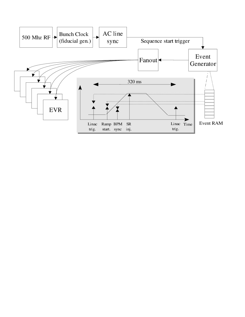
The reference generation is done with special purpose-built modules like a downconverter that divides the RF frequency to the fiducial signals of the machine. The event system is used to generate the sequence of events for the injection cycle and to distribute the timing to the relevant components. Practically the whole operation cycle is generated within the event generator from only one fiducial, namely one that tells when the number “0” buckets in the storage ring and booster are in alignment. The SLS injection sequence consists of about 20 events that are transmitted every 320 ms.
The event system is based on time-multiplexed transmission of event codes. The source is an event generator that transmits 8-bit event codes at the a frequency of 50 MHz over an optical link. Thus, the time resolution is 20 ns. The bitstream is multiplied to several branches with fanout modules. At each destination VME crate there is an event receiver that decodes the received event codes and performs the appropriate actions that are programmed for each event of interest to the particular crate.
Some subsystems like the linac have their internal timing. During construction the linac was required to have the ability to run standalone. The interface between the linac and the rest of the machine was defined to be the timing and RF signals. The synchronising timing to the linac is delivered with the event system; the linac cycle is triggered from an event.
The linac timing consists of the gun trigger system and the timing for the klystron modulators, prebuncher, gun RF amplifier and the 3 GHz frequency multiplier. This timing is achieved by using a pair of Stanford Research DG535 delay generators. The gun timing uses a number of TD4V delay cards [2], which also phase lock the trigger signals to the RF signal. The TD4V delay is programmable in units of RF cycles (2 ns) and is used to target specific RF buckets in the booster (and storage ring) and also to adjust the trigger pulse length. The trigger signal from these cards to the electron gun high voltage deck is delivered through an optical fiber using an Uniphase 51TA/RA transmitter/receiver pair.
3 TECHNICAL SOLUTION
To integrate all the desired functionality into one system, we decided to take the APS system as a model, but to upgrade to a recent technology: the Gigabit Ethernet. The requirement was to preserve the software compatibility so that we could take advantage of the software that was existing for the APS system.
The functional design was done in VHDL. This brought a big advantage: we could separate the hardware solution from the software interface, in a way that allows us a smooth upgrade path for both of the hardware and the software: when the communication technology has made an significant advance, we can port our model to the new technology without being tied to any particular technology or a component. And vice versa: any new ideas from the control system side can be implemented in firmware without any physical modifications (within the limits of the capabilities of the hardware.)
3.1 The hardware
The event system is based on Gigabit Ethernet technology, using a standard VCSEL short wavelength (860 nm) transceiver (drop-in replacement for long wavelength transceivers exist) and a gigabit transceiver chip. The transceivers allow for cascading several cards in a daisy chain. This way we can reduce the number of fanout branches and also build a sub-branch where another event generator is added to an upstream branch.
The logic resides in two PLDs, one CPLD and one FPGA (Xilinx Virtex). The CPLD handles the VME bus logic and configuration of the second one from Flash ROM. Flash ROM allows us to upgrade the systems in situ, even without powering down the system. This was a big advantage during development.
The event generator and receiver use the same PCB, with some different components fitted in depending on the card type. The event generator has, in addition to the common hardware, two 512 KB RAMs for “store and playback” of an event sequence, external clock and external trigger inputs. The event receiver has three extra outputs in the front panel. Their use is defined in firmware; presently they are used for reference frequency output.
The main clock for the event generator is downconverted from the main (500 MHz) RF. The downstream receivers synchronize automatically to the incoming bitstream. All the components are thus phase locked to the RF.
3.2 The firmware
The firmware for the cards is about 2000 lines of VHDL code for both of the modules (EVG, EVR). Being VHDL, it is independent of the particular type of chip (FPGA) used in the hardware implementation.
The main features were already present in the APS version, we extended them to provide more functionality to suit our operation scheme.
The most essential features of the event generator firmware are event RAM sequence handling, event priority resolver and the possibility to send event from software by writing into a register. The EVR has 4 channels with width and delay possibility, 14 channels with width adjustment only. Both of these have also a clock prescaler to scale down the clock and polarity selection. The EVR also has timestamp counter with the facilities for a synchronous reset and event FIFO mechanism for latching the timestamps when an event is received. For details, see [4].
The firmware for the event receiver uses about 95 % of the available gates on the Xilinx Virtex 150.
3.3 Interface to devices
Different devices require different signal types for the trigger pulses. Most devices have a TTL level input, some may have an NIM or ECL level input. Rather than trying to cover every possible requirement on-board, we decided to put the interface logic to an transition module according to the same philosophy as for other SLS controls interfaces. As an example, the power supplies for SLS [3] have an optical trigger input to run an internal waveform. For the power supplies, a transition module with optical outputs was designed.
3.4 Distribution system
The signals from the main timing source are distributed using an optical fiber fanout tree. The fanout is done with arrays of VCSEL transmitters. These are built as VME size cards that plug in the crate, but have no data interface. One card has one input and eight outputs, limited by the card size. To create more outputs, one can connect the cards in a tree configuration.
4 APPLICATIONS
4.1 Filling control
The timing system must be able to precisely control the filling of the storage ring. With the event system we could create a simple application to control the filling, without the need for any additional hardware and a few parameters to handle. The harmonic numbers of the SLS booster and storage ring are 450 and 480, respectively. This means that for each successive turn in the booster, the storage ring lags 30 RF buckets, until after 16 booster turns the same buckets are aligned again. This means that by shifting the extraction delay from the booster we can select the target bucket in 30 bucket steps. For the smaller steps we need to adjust the linac gun timing. Thus all that is needed to control the injection are two parameters: extraction delay and the linac gun delay. With the proper combination of these, all buckets in the storage ring can be reached.
The injector timing sequence is generated with the event RAM. The RAM clock is selected to be exactly one booster turn (450/500 MHz = 900 ns) and the cycle is started from a pulse that signals that the SR and booster RF buckets are in alignment. Changing the position of the extraction event in the RAM by one the extraction can be shifted by one turn, giving us the 30 cycle steps. The smaller steps are done by adjusting the linac gun timing. The linac timing controller is synchronized with the main timing. Knowing the next target bucket it calculate the required delay for the next cycle. The calculation and setting is synchronised with the injection with the corresponding event: the event triggers a software sequence to be executed on every injection cycle.
4.2 Top-up
Ability to do top-up injection was one of the requirements for the SLS from the beginning. This also sets several requirements for the timing system. The timing system has to be able to do single injection cycles, has to have the capability of sending gate signals to the beamline experiments and obviously, to synchronize several controllers that otherwise are interconnected only through Ethernet. The network connection cannot be relied on to transmit the command sequences in applications that are related to injection in real time. Basically, top-up is just an extension of the normal injection control application; it has to monitor the beam current, allow for setting of proper injection intervals and to have a capability to send advance notice to the beamlines before an injection.
4.3 Beamline timing
With our structure, we can simply extend the timing to beamlines by extending one fiber branch to an interested beamline, making all the timing signals available at the beamline. If the beamline has some special requirements, we can add one event generator to create a new sub-branch to create a tree-like structure. In this way, the beamline can add its own events but still have the whole machine timing information available.
5 CONCLUSIONS
The advances in technology have made it possible to build a timing system that can handle most of the timing tasks from commercial off-the-shelf components that are standardized and in wide use. The SLS timing system integrates most of the required timing functions into a single subsystem. The system is layered so that we could benefit from other earlier development but at the same time move to a one generation newer technology. The functionality is captured into a device independent language (VHDL), which allows decoupling of the functionality from the underlying technology, providing a smooth upgrade path for the next generations. The integration of the functions into a global system enables us to glue a distributed system into a single entity. This can greatly enhance the capabilities and operation of a complex system.
References
- [1] F. Lenkszus, R. Laird. “The APS Event System”, ICALEPCS 95, Chigago, June 1995.
- [2] T. Naito et.al. “Synchronization scheme for the KEKB”, ICALEPCS 97, November 1997.
- [3] A.Luedeke et.al.,”Digital Power supplies for the Swiss Light Source”, these proceedings
- [4] J. Pietarinen, “Event System”, available on-line at http://www.sls.psi.ch/controls/help/tutorials/subsystems/timing/