Effective Second Order Susceptibility in Photonic Crystals Composed from Centro-Symmetric Materials
Abstract
A technique for obtaining efficient bulk second order susceptibility in non centro-symmetric Photonic Crystals (PC) made from centro-symmetric materials is discussed. The effect is based on the electric quadrupole effect, strong electromagnetic mode deformation and non homogeneous contribution to volume polarization from different parts of the PC. The required symmetry breaking is introduced on the macroscale of the PC unit cell. The obtained structural is comparable with the second order susceptibility of ordinary non-linear materials. Phase matching can be achieved by introducing symmetry modulation (Quasi Phase Matching) during fabrication of the PC.
Optical materials with high second order susceptibility are frequently required for both fundamental and applied research. By utilizing three wave interactions in such media, existing coherent radiation sources can be extended to almost the entire optical spectrum. Consequently the importance of these materials can be compared with the importance of laser itself.
The number of efficient second order nonlinear materials is limited. To possess second order susceptibility the material has to be non-centro-symmetric. This immediately eliminates all amorphous materials and crystals from 11 of 32 symmetry classes. The choice between remaining materials is also limited due to different constraints: value of , absorption in required spectrum, damage threshold etc.
Different methods were proposed for development of enhanced non-linearity. The first is the search for new materials with large non-linear response on molecular or molecular arrangement[1] scales. The second is construction of composite materials[2]. In this case the effective enhancement is achieved due to redistribution of the energy inside composite structure. Unfortunately it can improve only , and not . Recently the use of Photonic Band Gap (PBG) crystals made from non-linear materials was proposed[3],[4]. All these methods require symmetry breaking on microscopic atomic or molecular dimensions.
In this Letter we describe a technique for obtaining efficient second order susceptibility in non centro-symmetric Photonic Crystals (PC) made from centro-symmetric materials. The effect is based on the electric quadrupole transition, strong electromagnetic mode deformation and different contributions to the volume polarization from different parts of the PC. The required symmetry breaking is introduced on the macroscale of the PC unit cell.
A local second order polarization can be obtained in centro-symmetric materials due to the quadrupole effect[5]. In quadrupole transitions the required symmetry breaking is obtained by asymmetry of the electromagnetic field spatial mode, rather than the asymmetry of the electron wave function as in the dipole transition case. The second order polarization corresponding to a quadrupole transition is:
| (1) |
where is a fourth-order tensor. Generally integration over the volume of such point polarization vanishes, due to periodicity of and gradient dependence of . Usually, only some weak signals from interfaces can be detected[6],[7], however the situation in PCs can be quite different.
PCs are artificial two or three dimensional periodic dielectric structures [8],[9]. They possess unique optical properties for electromagnetic radiation with wavelengths comparable with their period, including the existence of full PBGs, anomalously strong dispersion[10] and high photon localization near defects [11]. High dielectric constant modulation is required to obtain strong effects, so several technologies for construction of dielectric/air 2D [12], [13] and 3D[14], [15], [16] PCs have been developed.
Integration of eq. (1) over the volume in dielectric/air PC can be different from zero. The reason is unequal contributions to the polarization from different parts of the media. The polarization of the air regions can be totally neglected due to low electron density. Constructing PC in such a way that in dielectric part the has one sign and in the air the opposite, effective ”structural” volume polarization can be obtained.
Effective second order susceptibility induced by a quadrupole effect can be quite large [5]:
| (2) |
where , is the radiation wavelength, is some characteristic second order susceptibility, is characteristic interatomic dimension, is the modulation scale of electromagnetic mode (see Fig. 1) and is some numerical coefficient. can be as small as the radiation wavelength and . The origin of is that the dipole transition matrix element between states of different parity always has smaller numerical coefficient than quadrupole transition based on the matrix element of the same parity[5]. The experiments on the surface non-linear effect in Si, high index material which is used for PCs fabrication, show that in this material is only about three orders of magnitude weaker than of GaAs for [17]. It means that properly designed PCs made from Si, with non-vanishing contribution of in all the volume, can artificially provide second order susceptibility at least of the same order of magnitude as low second order coefficient uniform materials (e.g. quartz). The result may be even larger due to stronger modulation of the electromagnetic field in PC than at an ordinary interface and due to the influence of photonic band structure on electron transitions [4].
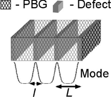
A specific realization of the desired material requires PCs with highly modulated electromagnetic mode. It can be achieved directly in some PCs, e.g. high mode modulation was predicted for silicon inverse opal structure [18], or by introducing periodic defects into the PBG substrate. The first approach may be realized using lower index materials, because the requirement for PBG does not exist. Unfortunately there were no intensive numerical search for photonic structures with high mode modulations and at these moment PCs of this type are not well explored. In contrast PBG crystals require high refractive index materials, but there are many known structures and almost any defect (extra or missing material, deviation from the periodicity) possesses localized modes for frequencies inside the gap, leading to modulated mode structure (see Fig. 1).
Also in the latter approach the required asymmetry can be achieved by proper defect’s design. Independent of the PBG substrate the defects should be asymmetric and possess dielectric/air structure. In the case when the electromagnetic mode is omnidirectional in dielectric part of the defect, the maximum volume contribution of polarization eq. (1) can be obtained. In our opinion, the hollow cavities, partially filled with the substrate’s material, are the best candidates for proposed method.
Let us now consider some specific example (see Fig. 2): Optical Parametric Oscillations (OPO) in a lattice of 1D defects (hollow waveguides) in 2D PBG environment. Such waveguides array can be fabricated using semiconductor lithography technology. To obtain a 2D PBG crystal, a hexagonal pattern of deep air columns can be etched in the high refractive index substrate, e.g. Si. During the same lithographic step the waveguides can be introduced by etching parallel stripes. Using quasicrystalline arrangement of air columns instead of hexagonal pattern, 2D PBG can be achieved in lower index materials, e.g. glass[19].
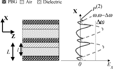
Inversion symmetry breaking is achieved by partial waveguide filling. It can be done by leaving an unetched stripe near each etched one(see Fig. 2). The possibility to guide electromagnetic modes in such waveguides is intrinsic property of PBG crystals. Guiding in PBG crystals has no crucial dependence on the internal waveguide’s structure, as in index guided modes, because the confinement of the electromagnetic mode exists only due to the external PBG environment.
Three electromagnetic waves (each TE mode): pump, signal and idler, propagate along the waveguides directions. Let us assume that pump and signal have almost degenerate frequencies and inside the forbidden gap. The idler’s frequency is assumed to be outside the gap (see Fig. 2).
Propagation of some specific radiation in a non-linear waveguide, can be described under slow varying amplitude approximation as[20]:
| (3) | |||||
| (4) |
where is an amplitude (), and are the frequency and wavevector of the mode, is the speed of light, is the normalized field distribution in the transverse plane, is transverse coordinate and is the induced non-linear polarization. For our specific model (see Fig. 2) the equation for the signal eq. (3) can be written as:
| (6) | |||||
| (7) |
using eq. (1) for and that the field of TE modes has only direction.
Under the assumption that the idler wavelength is larger than the defect’s size, can be assumed to be constant in the transverse plane. Under the same assumption the modes of pump and signal can be taken to be identical with some maximum on the dielectric/air interface inside the waveguide and zeros on its boundaries [11],[21] (see Fig. 2). In this case the integral in eq. (6) does not depend on the exact electromagnetic mode distribution, but on the field value at the boundary points of integration. The integral is tacken only over the filled part of the waveguide and can be evaluated analytically:
| (8) |
For an ordinary process eq. (6) becomes:
| (9) |
To compare eqs. (8) and (9) one must take into account that the energies of pump modes should be the same in both cases:
| (10) |
The ratio of effective non-linearities in these processes is:
| (11) |
It can be rewritten using eq. (2 ) and that as:
| (12) |
where indicates imperfect modes overlap in eq. (3). It can not affect the process seriously, since and can be of the same order ( is realistic) due to strong light confinement in PBG crystals, hence previously obtained estimations are valid for this specific PC.
For efficient conversion phase matching has to occur, in eq. (6). Otherwise the signal from different points along the propagation will interfere destructively. Generally in most materials this condition can be influenced only by change of the propagation direction.
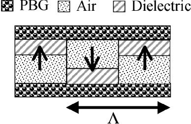
Phase matching can be achieved artificially by periodic modulation of the sign of the non-linear tensor coefficient. It can be achieved in ferroelectric crystals only by periodic poling. The method is called Quasi Phase Matching [22]. In non centro-symmetric PCs modulation of the non-linear coefficient can be introduced during fabrication (see Fig. 3).
These results can be extended to the general case of periodic lattice defects inside a PBG Crystal. As it was stated earlier single defects in PBG environments can possess localized modes for frequencies inside the gap. This means that for the same frequencies in periodic lattices of defects the mode can be not localized, but strongly modulated. Assuming that the electric field near the defects is and between them is , due to eq. (1) the scaling for structural polarization is:
| (13) |
where is the effective localization length of the mode and is the dimension of the defect’s lattice. This result is valid for the optimal case of field distribution, e.g. as in the previously considered example. The dimension of the defect lattice can be smaller than the space dimension. The periodicity of the entire crystal implies translational symmetry along all unconfined coordinates. Hence these coordinates can be omitted (see Fig. 1).
The ”structural” polarization has to be compared with the ordinary one:
| (14) |
where is the defect lattice constant. The ratio between and can be determined taking into account that the total energies of the compared modes has to be equal, similarly to eq. (10):
| (15) |
where is some numerical coefficient of order . Taking into account eq. (2) one can get:
| (16) |
The additional numerical coefficient corresponds to imperfect overlap of different modes [23]. In case of three wave interactions its scaling can be determined from eqs. (13, 14, 15) to be:
| (17) |
in the case of all waves being confined. Practically this can be difficult due to the finite forbidden gap in PCs. In case only two waves are confined and the scaling is:
| (18) |
where is the dimension of the defect’s lattice. For results (16) and (12) are equivalent. The obtained results are not limited to mode modulation by defects lattice, but the same formulae can be applied in the case of ”pure” PC strong mode modulation [18].
PC fibers[24] and so called ”Super Mirror”[25] waveguides are other good candidates for implementation of second order non-linear processes based on an electric quadrupole transition. They are suited for guiding light mode in the air, consequently the partial filling of these waveguides can provide effective second order non-linearity. Recently very interesting non-linear processes were observed in air/silica microstructure optical fibers[26]. Three dimensional defects are also highly interesting due to the analogy between 3D defects and molecules. All these cases require more extensive numerical investigation.
The measurement of the effects value can be completed by light propagation inside a properly designed PC, e.g. in the proposed waveguide’s array structure, or by light scattering from the surface of PC. In this case bulk and surface non-linearities can be distinguished by contribution of different light polarizations to the signal. In the case of surface non-linearity of centro-symmetric materials the tangential component of electromagnetic field does not contribute to generated harmonics of incident light.
Integrated optics is one of the possible applications for structural materials. Use of standard non-linear materials in integrated optics is difficult. Generally integration is either impossible due to incompatibility of different processes or expensive. The most convenient are polymers, but several specific disadvantages (e.g. lifetime) prevent their broad use. The method described above opens new possibilities for incorporating non-linear elements in optical chips by e.g. obtaining effective non-linearity from the chip substrate itself.
It was shown that a non centro-symmetric PC, made from substrates without bulk second order nonlinearity (amorphous materials or centrosymmetric crystals) can posses effective volume comparable with the second order susceptibility of ordinary nonlinear materials. The effect is based on the electric quadrupole transition and local enhancement of . The symmetry breaking is introduced on the macroscale of the unit cell of the PC, instead of atomic scale. The estimations were made for , and for smaller wavelengths the non-linearity should be stronger. Quasi Phase Matching can be introduced in the time of fabrication, so effective non-linear processes are feasible.
Discussions with Dr. G. Berkovich and Prof. Y. Silberberg are gratefully acknowledged.
REFERENCES
- [1] G.J. Ashwell, G. Jefferies, D.G. Hamilton, D.E. Lynch, M.P.S. Roberts, G.S. Bahra and C.R. Brown, Nature, 375, 385, 1995
- [2] G.L. Fisher, R.W. Boyd, R.J. Gehr, S.A. Jenekhe, J.A. Osaheni, J.E. Sipe and L.A. Weller-Brophy, Phys. Rev. Lett. 74, 1871, 1995
- [3] G. D. Aguanno, M. Centini, C. Sibilia, M. Bertolotti, M. Scalora, M.J. Bloemer and C.M. Bowden, Optics Letters, 24, 1663, 1999
- [4] S. John and K. Busch, J. Lightwave Technol., 17, 1931, 1999
- [5] N. Bloembergen and P.S. Pershan, Phys. Rev. 128, 606, 1962
- [6] P. Guyot-Sionnest, Y.R. Shen, Phys. Rev. B, 35, 4420, 1987
- [7] J.I. Dadap, J. Shan, K.B. Eisenthal and T.F. Heinz, Phys. Rev. Lett., 83, 4045, 1999
- [8] E. Yablonovich, Phys. Rev. Lett. 58, 2059, 1987
- [9] S. Jhon, Phys. Rev. Lett., 58, 2486, 1987
- [10] H. Kosaka, T. Kawashima, A. Tomita, M. Notomi, T. Tamamura, T. Sato, S. Kawakami, J. Lightwave Technol., 17, 2032, 1999
- [11] J. D. Joannopoulos, Pierre R. Villeneuve, Shanhui Fan, Nature, 386, 143, 1997
- [12] C.C. Cheng, A.F. Scherer, J. Vac. Sci. Technol. B, 13, 2696, 1995
- [13] C.J.M. Smith, H. Benisty, S. Olivier, M. Rattier, C. Weisbuch, T.F. Krauss, R.M. De La Rue, R. Houdre, U. Oesterle, Appl. Phys. Lett., 77, 2813, 2000
- [14] S.Y. Lin, J.G. Fleming, D.L. Hetherington, B.K. Smith, R. Biswas, K.M. Ho, M.M. Sigalas, W. Zubrzycki, S.R. Kurtz and J. Blur, Nature, 394, 251, 1998
- [15] S. Noda, K. Tomoda, N. Yamamoto and A. Chutinan, Science, 289, 604, 2000
- [16] A. Feigel, Z. Kotler, B. Sfez, A. Arsh, M. Klebanov and V. Lyubin, Appl. Phys. Lett., 77, 3221, 2000
- [17] N. Bloembergen, R.K. Chang, S.S. Jha and C.H. Lee, Phys. Rev., 174, 813, 1968
- [18] O. Toader, S. John and K. Busch, Optics Express, 8, 217, 2001
- [19] M.E. Zoorob, M.D.B. Charlton, G.J. Parker, J.J. Baumberg and M.C. Netti, Nature 404, 740, 2000
- [20] Y.R. Shen, The Principles of Nonlinear Optics, Jhon Wiley & Sons Inc., 1984
- [21] S.G. Johnson, S. Fan, P.R. Villeneuve and J.D. Joannopoulos, Phys. Rev. B, 60, 5751, 1999; M. Loncar, T. Doll, J. Vuckovic and A. Scherer, J. Lightwave Technol., 18, 1402, 2000
- [22] J.A. Armstrong, Phys. Rev., 127, 1918, 1962
- [23] A. Yariv, IEEE J. Quantum Electron., 9, 919, 1973
- [24] T.A. Birks, J.C. Knight, P.S. Russell, Optics Letters, 22, 961, 1997
- [25] E. Yablonovitch, Optics Letters, 23, 1648, 1998
- [26] J.K. Ranka and R.S. Windeler, Optics & Photonics News, August, 2000