[
Superconducting Nb-film LC resonator
Abstract
Sputtered Nb thin-film LC resonators for low frequencies at 0.5 MHz have been fabricated and tested in the temperature range 0.05 – 1 K in magnetic fields up to 30 mT. Their value increases towards decreasing temperature as and reaches at 0.05 K. As a function of magnetic field is unstable and displays variations up to 50 %, which are reproducible from one field sweep to the next. These instabilities are attributed to dielectric losses in the plasma deposited SiO2 insulation layer, since the thin-film coil alone reaches a Q at 0.05 K.
pacs:
PACS numbers: 85.25.Jw, 07.50.Yd, 61.43.Fs]
I Introduction
An electrical resonator with a high quality factor is a sensitive device for the measurement of materials’ properties. At low frequencies (up to several MHz) the inductive and capacitive elements are spatially separated and allow well-defined characterization of the magnetic or dielectric properties of the sample piece. Such resonators can be assembled from discrete components, i.e. a coil wound from superconducting wire and a high- capacitor [1]. With a parallel-coupled LC resonator, -values up to have been reached at temperatures below 0.1 K, when the solenoidal coil is wound from m Nb wire, and the resonator is directly coupled to the gate of a GaAs FET amplifier which is operated in a 4 K environment [2]. In our application the resonators have been employed for low-frequency continuous-wave NMR [3]. In most measuring applications a more efficient geometry for the resonators is a planar Nb thin-film construction where the inductively or capacitively coupled sample is sandwiched between two thin-film devices (Fig. 1).
The sensitivity of the measurement is often determined by the intrinsic losses of the resonator, i.e. by its unloaded value. The magnetic susceptibility of the sample changes the inductance
| (1) |
or equivalently in a capacitive measurement, the dielectric susceptibility is seen in the capacitance
| (2) |
The frequency-dependent complex susceptibilities, , consist of the dispersion and absorption . In the case of dielectrics, the dielectric constant is usually used: . and are constants which are defined by the thin-film component design. Usually the sample does not fill the entire active volume, which is accounted for by introducing a filling factor, to modify the effective susceptibility (see e.g. [4]).
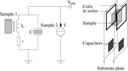
In Fig. 1 the resonator is driven from a constant current source and the output voltage is proportional to the impedance of the parallel LC circuit. The width of the resonance peak is determined by the losses, while the resonance frequency depends on the real component of the susceptibility . Both quantities can be extracted by recording the transfer function as a function of and by fitting the measured curve to the expected impedance of the equivalent circuit.
Frequently applications are in the limit where is small and one may use linear response at resonance. Then the sensitivity of the measurement improves with increasing . This limit is usually applied in continuous wave NMR measurement, where the resonator is driven at resonance and its output is modulated by taking the sample through magnetic resonance, by sweeping an externally applied magnetic field . Dispersion and absorption are then extracted from the resonance response [4]
| (3) |
In the case of a dielectric sample the frequency shift due to is typically large and requires retuning of the resonator from to . If we rewrite the dielectric constant in the form , where represents small changes in during the measurement, then the expression analogous to Eq. (3) becomes
| (4) |
where is the loss tangent and is assumed large.
II Design and fabrication
Our thin-film resonator design is shown in Fig. 2. These devices are meant for magnetic measurements where the sample is placed between two series-coupled planar coils on separate substrates, in a Helmholtz-like configuration. A static polarizing magnetic field is applied in the direction parallel to the two resonator plates.
The resonators are fabricated on mm silicon and sapphire wafers. The silicon wafers are cut from usual micro-fabrication grade n-doped single crystal material, with a 240 nm thick thermally oxidized SiO2 surface. The [112̄0] sapphire wafers, with an epitaxially polished surface, are used as reference substrates, to compare to a pure material with inherently low losses. The resonator circuit is fabricated in four layers which are summarized in Table I. In addition, a layer of Nb2O5, made by anodizing Nb in the lower Nb layer, is added to some capacitors, to test the properties of this dielectric.
The Nb layers are sputter deposited. The superconducting transition temperature of three 200 nm thick Nb test layers was measured to be 9.12 – 9.20 K, with a width of the transition region mK. The SiO2 insulation and passivation layers are deposited with plasma enhanced chemical vapor deposition (PECVD) from silane SiH4 gas. The first 50 nm are deposited at 120 ∘C and the rest at 150 ∘C. This process leaves typically a layer, which contains impurities such as OH- radicals, and its etch rate in HF acid is high.
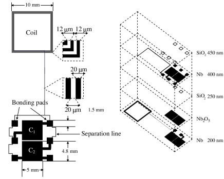
| Layer | Function | Material | Thickness | Fabrication |
| nm | method | |||
| 4 | Protection | SiO2 | 450 | PECVD |
| 3 | Conductor | Nb | 400 | Sputtering |
| 2 | Insulation | SiO2 | 250 | PECVD |
| 1b | Insulation | Nb2O5 | 140 | Anodization |
| 1b | Conductor | Nb | 150 | Sputtering |
| 1a | Conductor | Nb | 200 | Sputtering |
The dimensions of the resonator are shown in Fig. 2. The coil consists of 25 turns, with a linewidth and line spacing of 12 m. The coil was measured to have an inductance of 17 H at 4 K. The capacitor consists of a SiO2 layer ( at 4 K), sandwiched between two Nb films. The total capacitance of 8 nF is composed of two identical capacitors, connected with lines which can later be cut, similar to the connection between the capacitance and inductance. This allows to sample the uniformity of the fabricated components and to operate the resonator in different configurations. The bonding pads are designed to be large, to allow easy electrical connections.
Before use, the resonators are screened in room-temperature resistance measurements for fabrication failures. Less than 10 % of the capacitors show very low resistance and are assumed short circuited. The expected value for the coil resistance is 106 k at room temperature. However, only about 20 % of the coils reach this value. Others have a reduced resistance indicating that a parallel shunt resistance exists across some turns in the coil. In this respect the most delicate section of the present design is the return lead from the center of the coil in the top most Nb layer. This lead crosses all 25 turns of the coil winding, with 50 steps in layer height. In most cases coils with a reduced resistance at room-temperature recover the proper value of 30 k on cooling to 77 K. To cure problems with the SiO2 insulation, some resonators were annealed at C for 2 h. This turned out detrimental to the Nb film. Other annealing efforts at a lower temperature of C were equally unsuccessful. Otherwise the resonators are durable, both with respect to storage at room temperature and thermal cycling to 4 K.
III Measurement setup
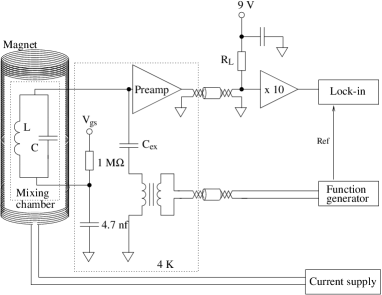
The measuring setup is shown in Fig. 3. The resonator is placed inside the mixing chamber of a small 3He–4He dilution refrigerator which cools to 50 mK. To minimize losses, the resonator is housed in an extension of the mixing chamber which is machined from araldite epoxy. A heat treated high-conductivity copper shield is inserted between the mixing chamber and the steel vacuum jacket, to reduce dissipation in the metal parts. A superconducting solenoid outside the vacuum jacket in the liquid He bath is used to generate a homogenous magnetic field parallel to the Nb film.
Ultrasonic bonding with m Al alloy wire is used to connect to the bonding pads on the resonators. High values are achieved, even when the bonding wire is part of the resonance circuit with two Nb-film coils connected in series. This indicates good contact of the bonding wire to the Nb pad. Unfortunately the Al alloy loses its superconductivity at a low magnetic field ( mT).
The voltage across the resonator is measured with a FET preamplifier operating at 4 K in the liquid He bath, similar to that described in Ref. [1]. The resonator is connected to the preamplifier via a twisted pair of superconducting wires. The resistance in these leads outside the resonator loop is not critical since most of the current flow occurs within the resonator. The resonator is excited via a transformer and a coupling capacitance . This represents a nonideal current source, especially for a high- resonator, but it can be shown to be equivalent to an ideal source if the resonator capacitance is replaced with an effective capacitance . Thus the feeding capacitor needs to be small with high , not to load the resonator.
The liquid-He-temperature preamplifier is an integral part of the resonator since measurements with values approaching are not possible without a high-input-impedance device. Even so, we find that the input FET has a leak resistance and parasitic capacitance which load the resonator at the highest impedance levels. In the present measurements the total noise reduced to the input of the preamplifier is .
IV Results on values
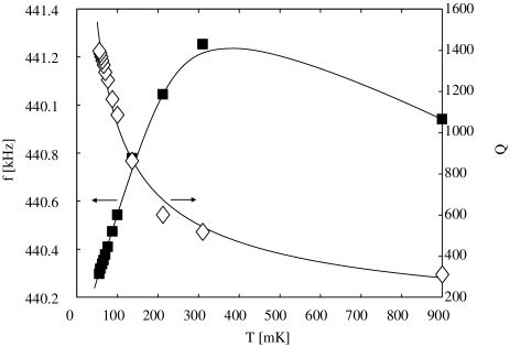
In Fig. 4 the temperature dependences of and the resonance frequency are shown for a single resonator of the type shown in Fig. 2, with only SiO2 insulation in the capacitors. The values turned out to be low, (1 – 2) at 50 mK, on both silicon and sapphire substrates, and within measuring precision did not depend on the resonance excitation level in the regime 0.01 – 1 mV across the resonator (at constant applied magnetic field). The resonance frequency has a maximum at about 400 mK, which corresponds to a minimum in the dielectric constant of the SiO2 insulation in the capacitors.
To resolve the origin of the low value, the thin-film components were tested separately. If the thin-film coil on the resonator plate is replaced with an external wire-wound Nb coil with a similar inductance and high value, then the resonator is not significantly changed from those recorded in Fig. 4. In contrast,
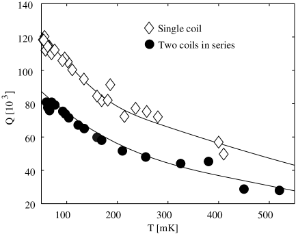
when the thin-film capacitance on the resonator plate is replaced with external low-loss capacitors [5], much higher values are measured, as shown in Fig. 5: climbs at 50 mK to with a single thin-film coil and to with two coils on different resonator plates coupled in series with Al bonding wires. Thus the thin-film coils perform well, at least in terms of their value. On warming to 500 mK, the value drops by a factor of 3, which is approximately the same behavior as for the complete thin-film resonators in Fig. 4. With external capacitances the change in resonance frequency is small, Hz, compared to kHz in Fig. 4. From these test we conclude that the losses of the resonator are dominated by the SiO2 insulation layer in the capacitors.
Finally, it is instructive to note that the high values in Fig. 5 are sensitive to the preamlifier bias settings. Fig. 6 shows the dependence on the gate-to-source voltage of the input FET. An equivalent circuit for the FET input [6] is shown in the inset where the input is replaced with a parasitic capacitance Cp and a shunt resistance which both are connected in parallel to the resonator. Their values depend on the FET bias settings.
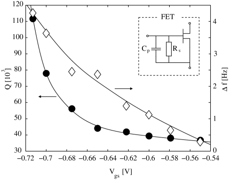
The change in capacitance, as calculated from in Fig. 6, corresponds to 0.1 pF. To obtain the measured , the input resistance would be M in the case of an ideal resonator. Since the resonator is not ideal, the FET input resistance is higher. Assuming, as an example, the resonator to be , then the input resistance of the FET needs to be 30 M, to produce a loaded of 1.2.
V Magnetic field effects
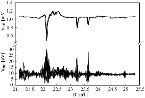
The resonators turned out to be highly sensitive to applied magnetic field. Fig. 7 shows an example where the voltage across the resonator is recorded at resonance as a function of magnetic field. The resonance frequency is not substantially changing during the measurement, thus the changes in output voltage are due to absorption and correspond roughly to similar changes in value. The output is not reproducible from one resonator to the next, but reproduces from one measurement to the next as a function of field for one particular resonator. At low excitation (bottom panel) the changes in output voltage as a function of field have the appearance of noise, with both positive and negative changes from the average. At higher excitations (top panel) the changes look more like reductions in value. The output appears to be independent of the sweep rate of the magnetic field and if the sweep is stopped, then the last value is preserved. The unstable behavior continues all the way to zero magnetic field.
The magnetic field dependence of is present in similar magnitude in resonators on both silicon and sapphire substrates, also with and without the extra Nb2O5 insulation. If the thin-film coil is replaced with a high- wire-wound coil, then the output as a function of field remains unchanged. In contrast, a thin-film coil connected in parallel with external high- capacitors produces a much more stable output as a function of field (at a much increased value). However, the thin-film coil also suffers from the magnetic field dependence, although to a smaller extent. For instance, with the two thin-film coils in series in Fig. 5, the changes in output voltage are % at 62 mK, where . In addition, the thin-film coil exhibits a monotonous drop in Q value as a function of magnetic field. A measurement on the series connection of two thin-film coils at 63 mK showed a at zero field which dropped by about 10% when the field was increased to 7 mT, while the resonance frequency remained unchanged to within 1 Hz. This is a sufficiently small change that it would not be measurable for the complete resonator, where the low value is determined by the capacitors. In the last example the bonding to the coils was done with Al alloy wire. This results in a drastic drop in Q when the bonding wire loses its superconductivity above 8 mT.
Our measurements suggest that the unstable magnetic field dependence originates primarily from the SiO2 insulation: The effects are strong when the thin-film capacitors are used. The thin-film coil has a small parasitic capacitance of about 0.3 pF, which also involves the SiO2 insulation: This capacitance arises when the lead from the center of the coil crosses over all the turns of the planar windings. Thus the magnetic field effects of the complete thin-film resonator and those of the thin-film coil alone are scaled roughly in proportion to their capacitances with SiO2 insulation. Similar magnetic-field-dependent effects have been observed previously in thin-film coils of much smaller size [7].
VI Amorphous thin-film insulator
Both the reduced Q of the resonators and their unstable losses as a function of magnetic field have here been traced to originate primarily from the amorphous PECVD-deposited SiO2 insulation in the capacitors. Amorphous dielectrics are known to be lossy and to exhibit as a function of temperature a minimum in the dielectric constant at a few hundred mK [8], as was the case here. Recently the dielectric constant of the multicomponent glass BaO-Al2O3-SiO2 has been reported to be sensitive to magnetic fields at temperatures of a few mK [10, 9]. These measurements were conducted at 1 kHz, whereas here we operate at a higher frequency of 400 kHz. The dielectric constant has also been found to be sensitive to the excitation amplitude [11]. With our low excitation levels, we did not find significant dependence of the average dielectric losses or the resonance frequency on the applied ac electric field in the measurements of Figs. 4 or 5.
In addition to the amorphous structure of the insulation layer, impurities, or the interface between the dielectric and the Nb may also contribute to the observed effects.
VII Conclusions
The present work shows that Nb-film fabrication methods turn out a good yield of durable resonators, and that the sputtered Nb film is a high-quality conductor on a standard doped silicon substrate at frequencies of about 1 MHz at mK temperatures. In contrast, PECVD deposited SiO2 insulation does not reach corresponding quality levels: Its dielectric losses are large and highly magnetic field dependent, even around zero field. Additional anodized Nb2O5 insulation did not increase the losses and might be of better quality.
Secondly, the thin-film inductor is of sufficiently high quality such that it can be used to investigate the properties of the dielectric in the capacitor, to find better alternatives. The resonator method with a high-Q coil and a GaAs MESFET preamplifier thereby allows access to the frequency range from 0.1 MHz up to several MHz, which so far has been only rarely investigated in studies of amorphous solids.
Acknowledgements
This work was funded in part by the EU-IHP programme (contract no. HPRI-1999-00098). We thank the personnel at the Microelectronics Centre for their help with the fabrication of the resonators.
REFERENCES
- [1] V.M. Ruutu, J. Koivuniemi, Ü. Parts, A. Hirai, and M. Krusius, Physica B 194-196, 159 (1994).
- [2] J. Koivuniemi and M. Krusius, Physica B 284-288, 2147 (2000); ibid. p. 2149.
- [3] V.M. Ruutu, Ü. Parts, J.H. Koivuniemi, N.B. Kopnin, and M. Krusius, J. Low Temp. Phys. 107, 93 (1997).
- [4] A. Abragam, The Principles of Magnetic Resonance (Oxford University Press, Oxford, UK, 1961).
- [5] High-Q surface-mount capacitors: Spectrum Control Inc., 6000 West Ridge Road, Erie, PA 16506, USA. A parallel connection of four 1 nf Ultra-Q chip capacitors is used.
- [6] The active components in the preamplifier are SONY 3SK165 GaAs MESFETs [1].
- [7] J. Koivuniemi, M. Kiviranta, H. Seppä, and M. Krusius, J. Low. Temp. Phys.110, 255 (1998).
- [8] F. Pobell, Matter and methods at low temperatures (Springer Verlag, Berlin, 1992).
- [9] P. Strehlow, M. Wohlfahrt, A.G. Jansen, R. Haueisen, G. Weiss, C. Enss, and S. Hunklinger, Phys. Rev. Lett. 84, 1938 (2000).
- [10] P. Strehlow, C. Enss, and S. Hunklinger, Phys. Rev. Lett.80, 5361 (1998).
- [11] S. Rogge, D. Natelson, B. Tigner, and D.D. Osheroff, Phys. Rev. B 55, 11256 (1997).