Lorentz angle measurements in irradiated silicon detectors
between 77 K and 300 K
Abstract
Future experiments are using silicon detectors in a high radiation environment and in high magnetic fields. The radiation tolerance of silicon improves by cooling it to temperatures below . At low temperatures the mobility increases, which leads to larger deflections of the charge carriers by the Lorentz force.
A good knowledge of the Lorentz angle is needed for design and operation of silicon detectors. We present measurements of the Lorentz angle between and before and after irradiation with a primary beam of 21 MeV protons.
, , , , , , , , , , , and
1 Introduction
Future collider experiments need stronger magnetic fields for momentum measurements, because of the higher particle momenta. In high fields the drifting charge carriers generated by traversing particles are deflected significantly by the Lorentz force , where is the drift velocity and the magnetic field. As advantage of such a deflection one can consider the improved charge sharing between the readout strips, which can improve the resolution for a given readout pitch. On the other hand the charge sharing worsens the double track resolution and the signal-to-noise ratio. As is well known[1, 2, 3, 4], the drift mobility of electrons is larger than the hole mobility, which yields a considerably larger Lorentz shift for electrons than for holes. Therefore, silicon detector with charge integration on both sides, show much less of an effect of the magnetic field on the p-side, where the holes are collected, than on the n-side, where the electrons are collected.
Typical position resolutions of silicon strip detectors are in the order of , while the Lorentz shifts in a 4 T magnetic field reaches 200 for electrons in a 300 thick detector. Therefore, these shifts have to be accounted for and an interesting question is the dependence of the Lorentz shift on the irradiation dose. For an LHC experiment, where the dose reaches over particles per , the change in drift mobility due to the defects introduced by the radiation damage, might result in a continuous change of the Lorentz shift, and thus of the calibration of the detector.
The radiation tolerance of silicon detectors can be improved by either oxygenating the wafers[5] At lower temperatures the mobility of both electrons and holes increases rapidly () and Lorentz angles for electrons up to 80∘ were observed in a 4 T magnetic field at temperatures of 80 K[3].
In this paper we study the Lorentz angles of both electrons and holes in magnetic fields up to 8 T and temperatures between 77 and 300 K. This is done before and after irradiating a detector with 21 MeV protons up to a fluence of , which equals 1 MeV equivalent neutrons.
2 Experimental setup
The Lorentz angle under which charge carriers are deflected in a magnetic field perpendicular to the electric field is defined by:
| (1) |
where the drift length corresponds to the detector thickness and the shift of the center of charge is (see figure 1). The Hall mobility is denoted by , the conduction mobility by . The Hall mobility differs from the conduction mobility by the Hall scattering factor . This factor describes the influence of the magnetic field on the mean scattering time of carriers of different energy and velocity[7]. The Hall scattering factor has a value of 1.15 (0.7) for electrons (holes) at room temperature and decreases (increases) towards with decreasing temperature [8]. The mobility increases with temperature proportional to [9].
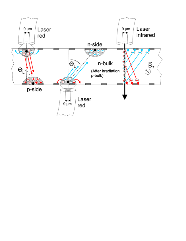
The Lorentz angle can be measured by injecting charges at the surface on one side and observing the drift through the detector by measuring the position of this charge on the opposite side(see figure 1). Charges were generated by injecting light with a wavelength of , which has an absorption length of at and at . Alternatively an infrared laser with a wavelength of 1060 nm was used, which has an absorption length of 300 at room temperature. This laser penetrates the detector and so mimicks a minimimum ionizing particle. With the red laser one type of carriers immediately recombines at the nearest electrode, whereas the other type drifts towards the opposite side. This allows to measure the Lorentz angle for electrons and holes separately by either injecting laser light on the n- or p-side.
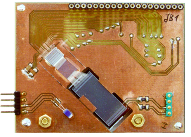
For our measurements the JUMBO magnet from the Forschungszentrum Karlsruhe[10] was used in a configuration with a warm bore of 7 cm. A flow of cold nitrogen gas through the warm bore allowed the detectors to be cooled to temperatures between 77 and 300 K. The sensors are double sided “baby” detectors of approximately 2x1 cm from the HERA–B production by Sintef. They have a strip pitch of 50 micron on the p–side and 80 micron on the n–side; the strips on opposite sides are oriented at an angle of 90 degree with respect to each other. The x- and y-directions are taken to be along the strips, while the E-field is in the z-direction. The B-field, perpendicular to the electric field, has to be in the x-y plane, but cannot be oriented along the x- or y-direction, since then the Lorentz shift would be along one of the strips, i.e. unmeasurable. Therefore, the detector is rotated 45 degrees, so that the B-field direction is at an angle of 45 degrees with both the x- and y-axis, as shown in fig. 2. The sensor is glued on the hybrid together with a pitch adapter and a 128 channel Premux charge sensitive amplifiers[11] on each side. The conections are standard wirebonds. All signals are digitized for every laser pulse and averaged over a few 100 pulses.
The signal position is computed using either the center of gravity or a Gauss-fit:
| (2) |
Here is the pulse height of the strip and its position.
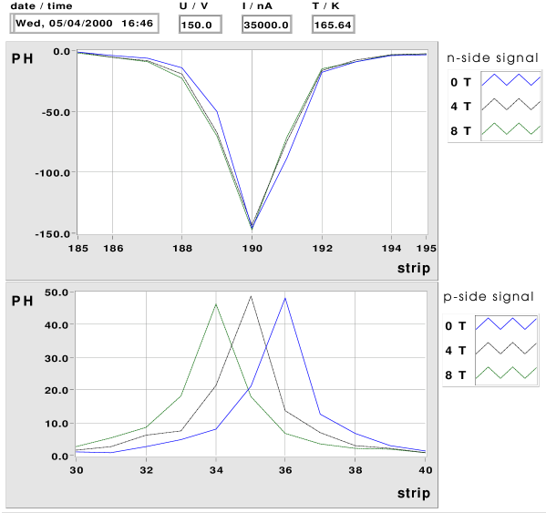
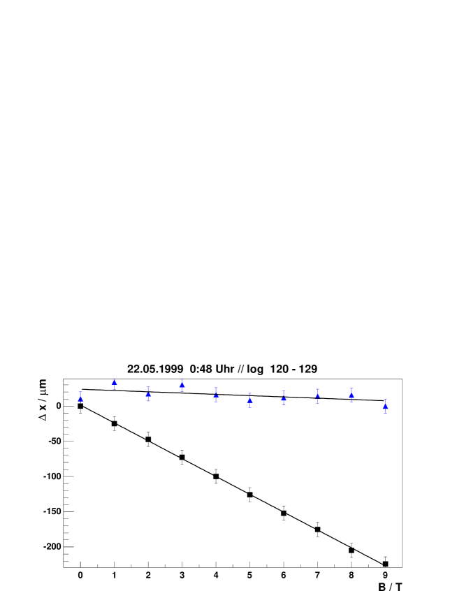
As can be seen from figure 3, the pulse on one side hardly moves due to the immediate recombination, while the pulse on the opposite side shows a clear Lorentz shift. The signal position is plotted as a function of the magnetic field in figure 4, which shows clearly that the Lorentz shift is linear with the magnetic field up to 9 T.
In order to better understand the drift in the detector simulations were performed with the Davinci software package by TMA[12]. The inhomogeneous electric field in the sensor was taken into account by following the charge in small steps, calculating the mobility at each position and integrating the Lorentz shift using eq. 1 with a Hall scattering factor of and for electrons and holes, respectively. These are the values expected for highly resistive sensors, in which the scattering by phonons dominates over the scattering by impurities[9].
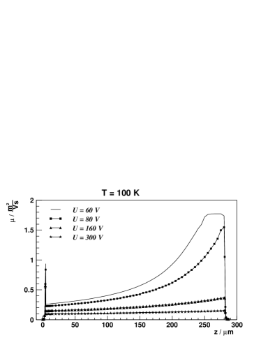
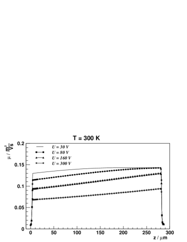
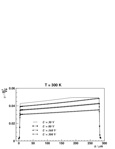
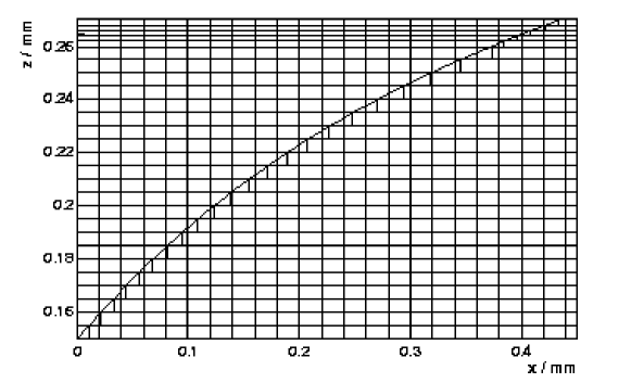
For bias voltages at least a factor two above the depletion voltage the mobility is practically constant in the detector, while for just depleted detectors the mobility increases in the regions, where the electric field goes to zero, especially at low temperatures, as shown in figure 5. The corresponding mean trajectory of the ionization becomes non linear, as shown in figure 6.
3 Results
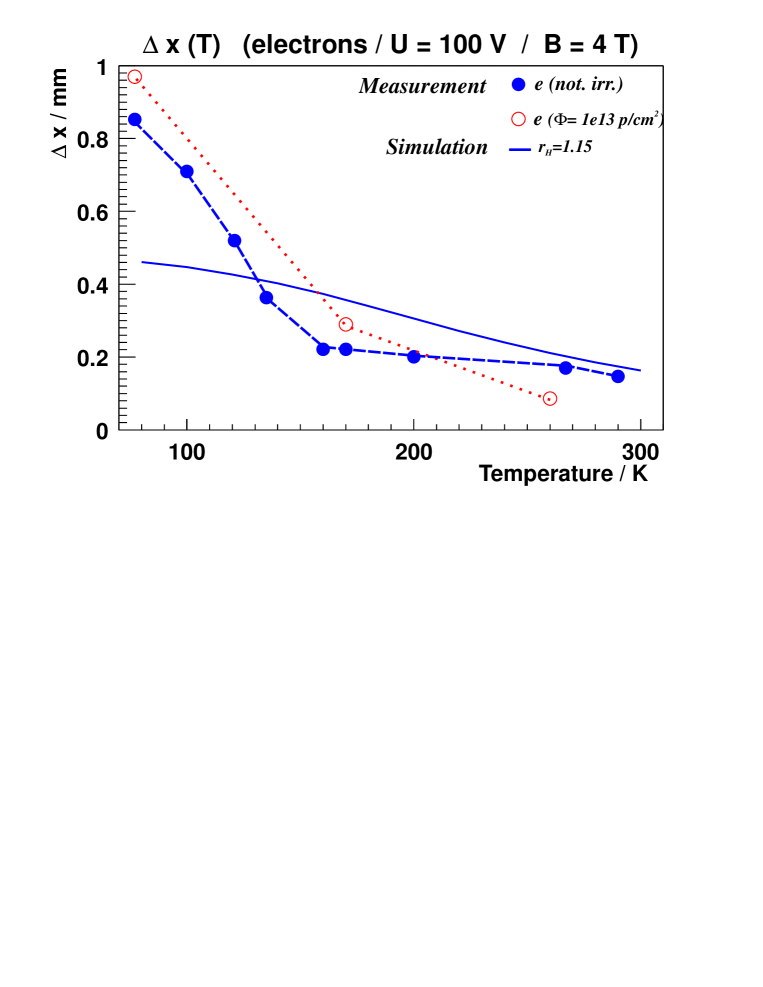
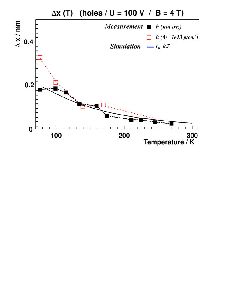
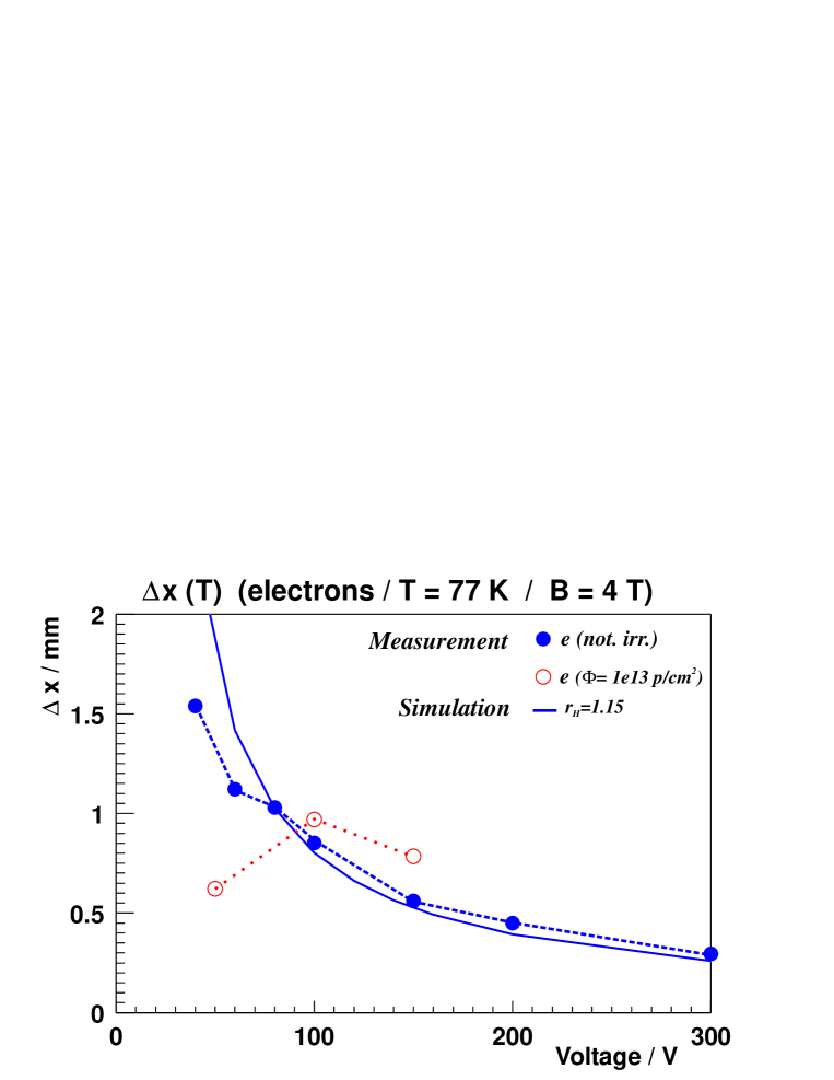
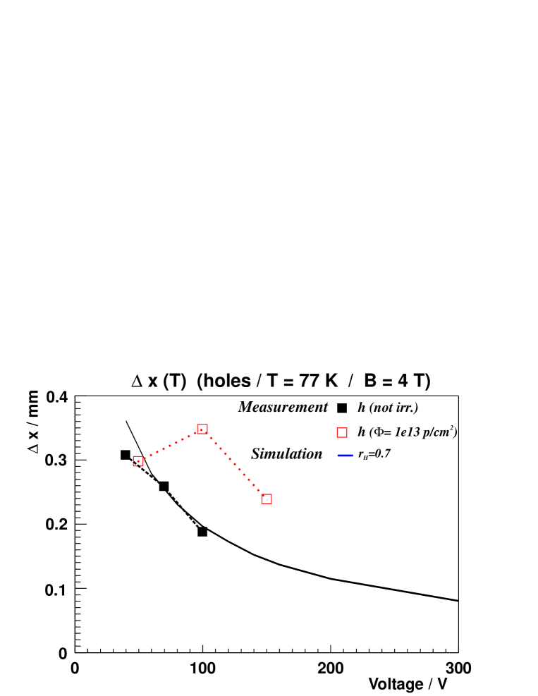
Instead of the Lorentz angle the shift in a thick detector is plotted for a 4 T magnetic field, which is the one of interest for future experiments. The dependence on temperature and bias voltage is shown in figures 7 and 8 together with the simulations from the Davinci software package by TMA[12], as mentioned above.
For holes the temperature dependence is well described, but for electrons the Lorentz angle first falls below the simulation for decreasing temperature, as expected for a decreasing value of the Hall scattering factor at lower temperatures[8]. However, below K the Lorentz angle for electrons rapidly increases and is a factor two the simulation at liquid nitrogen temperature. The simulation was done with a temperature independent Hall factor of 1.15 (0.7) for electrons (holes), which is certainly wrong[8]. Therefore, the most likely interpretation of the deviation between simulation and data would be the temperature dependence of the Hall scattering factor, since the drift mobility at low temperatures is well known[8] and the electric field dependence is well described by the simulation, as shown in figure 8. However, if the data is a factor two above the simulation at low temperature, then a Hall scattering factor around two is needed. Such a large is expected for impurity scattering[7], but this cannot be reconciled with the high resistivity silicon used for the sensors, for which the impurity doping is less then .
Before irradiation the detector depletes fully with a bias voltage of 40 V, while after radiation with 21 MeV protons per the depletion voltage has increased to 100 V. This implies that the bulk is inverted from n-type to p-type material, as expected[5]. The bulk damage of 21 MeV protons is about 2.8 times the damage by 1 MeV neutrons. The decrease of the Lorentz shift for the irradiated sample below 100 V in figure 8 is due to the reduced effective thickness of the partially depleted detector. Numerical results on the Lorentz angles and Lorentz shifts have been summarized in tables 2 and 2 before and after irradiation, respectively.
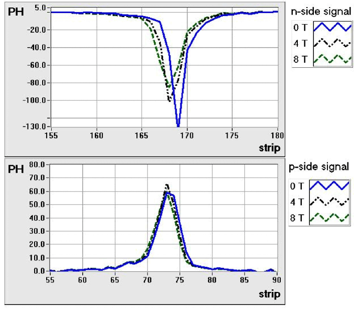
Figure 9 shows the signal from the 1060 nm infrared laser on the irradiated detector. As mentioned before, this laser has an absorption length of about 300 at room temperature, so it traverses the detector. It can be seen that the signal on the p-side hardly moves with the magnetic field, as expected for a dominant contribution of holes by the charge integrating amplifier, while the n-side shows a Lorentz shift corresponding to roughly half the Lorentz shift of the red laser. This is expected for ionization distributed in the detector, so the average drift length is half of the detector thickness.
4 Conclusion
The Lorentz angle has been measured for electrons and holes separately. For the non-irradiated detector the Lorentz angles of holes agree with simulations at all temperatures, but for electrons the Lorentz angle agrees only at room temperature. Below the angle increases rapidly to twice the expected value. A possible explanation could be a Hall scattering factor of instead of , although this is in contrast to the expectation for our high purity silicon sensors, where one expects to approach one at low temperatures.
After irradiation, the Lorentz angle for holes is hardly changed at room temperatures, at least if the bias voltage is raised to obtain full depletion again. However, for electrons the angle decrease 25% at room temperature. At lower temperatures radiation damage increase the Lorentz angles, both of electrons and holes.
Silicon detectors in high magnetic fields at cryogenic temperatures can be used without problems, if only the p-side (holes) is read-out. For an n–side read-out the too large Lorentz angles can be avoided, if the strips are oriented such, that the Lorentz shift is parallel to the strips. If this is not wanted, the Lorentz angle can be reduced by overbiasing the detector.
5 Acknowlegdements
This work was done within the framework of the RD39 Collaboration[6]. We thank Dr. Iris Abt from the MPI, Munich, Germany for supplying us with double sided strip detectors from the HERA-B production by Sintef.
| Electrons (280 K) | Holes (270 K) | Electrons (77 K) | Holes (77 K) | |||||
| Bias / V | ||||||||
| 40 | 192 | 34 | 1539 | 309 | ||||
| 100 | 170 | 38 | 852 | 184 | ||||
| 200 | 31 | 449 | ||||||
| 300 | 25 | 295 | ||||||
| Electrons (280 K) | Holes (260 K) | Electrons (77 K) | Holes (77 K) | |||||
| Bias / V | ||||||||
| 50 | 117 | 45 | 630 | 297 | ||||
| 100 | 127 | 42 | 970 | 329 | ||||
| 150 | 126 | 40 | 785 | 228 | ||||
References
- [1] E. Belau et al., Nucl. Instr. Meth. 214 (1983) 253
- [2] F. Röderer, Diplomarbeit, Univ. of Karlsruhe, IEKP–KA/98–24 (in german only).
- [3] S. Heising, Ph. D. thesis. Univ. of Karlsruhe, IEKP–KA/99–26 (in german only).
- [4] F. Hauler, Diplomarbeit, Univ. of Karlsruhe, IEKP–KA/2000–12 (in german only).
- [5] RD48 collaboration, http://rd48.web.cern.ch, ROSE/TN/2000-03.
- [6] RD39 Collaboration, Nucl. Instr. and Meth. in Phys. Res. A 440 (2000) 5-16 and http://rd39.web.cern.ch, RD39 Status Report CERN/LHCC 2000-010, 06-Jan-2000.
- [7] R.A. Smith, Semiconductors, Cambridge Univ. Press, 1968
- [8] Landolt-Börnstein, Numerical Data and Functional Relationships in Science and Technology, Group III, Band 17a, Springer Verlag, Berlin, 1982.
- [9] S. Sze, Physics of Semiconductor devices, John Wiley and Sons, 1981.
- [10] F. Hornung, A. Rimikes, Th. Schneider, High Magnetic Field facilities and Projects at the Forschungszentrum Karlsruhe, Internal Note, 1999.
- [11] L. Jones, Premux128 Specification, version 2.3, Rutherford Internal Note, 1995.
- [12] Technology Modelling Associates, Inc.: Davincie, Version 4.1, July 1998.