Design and Simulation of a High Frequency High Power Rf Extraction Device Using a Dielectric-Loaded Waveguide
Abstract
We consider the use of a dielectric-loaded structure to extract rf energy from a high current electron drive beam as a power source for a high energy two-beam accelerator. This represents an alternative technique which we show to have some significant advantages over the use of the currently proposed corrugated metal structures as power extraction devices. We discuss a particular design that will extract high power rf (0.1 – 1 GW) from a high current drive beam. Rf generation and transport in this class of devices have already been demonstrated at lower frequencies. We discuss the design parameters for 15 and 30 GHz dielectric transfer structures and some possible experiments.
keywords:
wakefield, linear collider, rf structuresPACS:
41.75.Lx,41.60.Bq,84.40.-x,29.17.+w1 Introduction
One trend in proposed future high energy linear collider designs is the use of high accelerating gradients in room temperature high frequency structures. This approach has the advantage that the average rf power for a given accelerating gradient scales as 1/(frequency)2 R1 , while the breakdown field is empirically found to scale approximately as (frequency)1/3 R2 . At the same time, the technology of conventional (klystron) rf sources is difficult to implement at frequencies higher than X-band (11.4 GHz) R1 . Two- beam acceleration R3 overcomes this difficulty by using a conventionally accelerated high current drive beam as the rf source for the high energy accelerator.
Two beam acceleration requires generation and propagation of a high current drive beam, and an efficient transfer structure to extract energy from the drive beam. We propose that a dielectric loaded waveguide represents an optimal power extraction/transfer structure. Dielectric structures have been investigated experimentally at some length R4 ; R5 . We summarize some of the important features of this class of devices compared to conventional copper rf structures:
-
•
Simplicity of construction. As shown in figure 1, the structure is a simple ceramic tube which is inserted into a conducting copper sleeve.
-
•
Higher order mode damping. Parasitic HEM modes generated by off-axis injection errors can be easily suppressed R6 by interrupting the outer conductor with axial cuts and surrounding the sleeve with an absorbing material. Note that this technique requires no modification to the dielectric tube and only modest machining of the exterior conducting sleeve.
-
•
Recent advances in dielectric materials for microwave applications. Very low loss () and high Q materials are commercially available R7 .
Other issues which may represent possible limitations on the performance of dielectric structures are actively being investigated:
-
•
Efficient rf coupling. The wakefield generated by the drive beam must be coupled out to a rectangular waveguide for transfer to the accelerating structure. This involves a mode conversion from TM01 in the dielectric tube to TE in the waveguide. Significant progress on efficient coupling design has been made R8 .
-
•
Charging. Beam halo or missteered beam impinging on the dielectric tube can cause large electrostatic charge buildup, resulting in deflection of the beam or volume breakdown of the structure. We have observed both these effects in our experiments using polymer based materials such as rexolite or nylon but have not observed this in any of the glass or ceramic materials we have tested. Changes in microwave dielectric properties with time due to radiation damage have also not been seen in our experiments.
-
•
Rf breakdown. The work in this area has been almost entirely confined to copper structures R2 . We have currently generated rf surface fields in ceramic structures 10 MV/m at 15 GHz R5 (limited by the available drive beam properties); no breakdown was observed at this level. We expect that significantly higher fields can be developed at these frequencies before breakdown occurs but it is worth pointing out that these devices are interesting as power extraction structures even at 10 MeV/m scale gradients.
2 Rf Power Generation in a Dielectric Structure
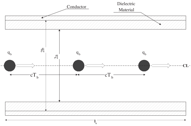
We follow the approach and notation of reference R9 . Consider a dielectric structure (figure 1) with inner radius a and outer radius b. An electron bunch train passing through the device will generate a steady state RF power
| (1) |
where is the length of the structure, is the charge/bunch, is the bunch separation, is the group velocity and is a form factor proportional to the bunch spectrum (assumed Gaussian). is the normalized ratio of the shunt impedance of the structure to its quality factor and encapsulates all the details of the structure geometry.
To compute for a dielectric structure, we use
| (2) |
where is the longitudinal decelerating wakefield in the device. In the limit of an infinitely long structure, the analytic expression for the wakefield is given in R10 . This provides via equation 2, and we can proceed to compute and optimize the properties of our structures.
Since the formalism of reference R10 does not allow for the effects of structure boundaries, rf coupling etc., it only yields an approximate evaluation of the properties of these structures. We will also give more accurate results of numerical calculations which include finite structure length and rf extraction effects.
3 Design of the Dielectric Power Extraction/Transfer Structures
In this section we give a reference design for both 15 and 30 GHz structures. While the choice of device parameters are not identical to the CLIC final design, this work allows the study of the physics and engineering aspects of dielectric- based power extraction devices. We have attempted to develop power levels of 100 MW with large coupling to the beam and using a common, commercially available dielectric.
While 30 GHz is the design frequency of CLIC R9 , there are a number of advantages in developing a 15 GHz structure first. The lower frequency is compatible with both the microwave measurement equipment and the beam spectrum available at the AWA R5 . Also, there is some question whether the use of 30 GHz rf does in fact provide significant performance improvement over 10 GHz range devices R11 .
The choice of dielectric is Cordierite which has a relatively low permittivity (4.5) and low losses (Q=5000, ). This material is commercially available R7 , and we have verified its dielectric properties in bench tests.
The choice of dielectric is not unique; for example, steatite, another commercially available material, has a permittivity of 5.8 and loss tangent of 0.0001 and would perform equally well. Theoretically one could also use a low coupling strength using a thin layer of high permittivity material to line the structure wg .
The inner radius a must be chosen to transport all the drive beam. The choice of dielectric material and the device frequency then fix the outer radius b. Using the methods outlined previously, we can calculate and power generated in these devices assuming CLIC test facility beam parameters.
Because of the simple geometry, the structures will be easy to machine. Conservatively assuming that the outer and inner radii of the structures can be machined to a tolerance of 25 m, the worst case deviations from nominal frequency due to this tolerance are 3.4% for the 30 GHz device and 1.5% for the 15 GHz structure.
4 Numerical Calculations
We also used the finite difference time domain program ARRAKIS R12 to calculate the power generated in these structures while taking into account the finite structure length, group velocity of the wakefield, etc. In order to simulate the effects of power extraction from the structure, an absorbing boundary was placed at the downstream end of the dielectric tube in the computational geometry.
Figures 2a and 3a show the longitudinal wake potentials for the 15 and 30 GHz devices for a single drive bunch and for a train of 1 nC bunches spaced by 10 cm. Buildup of fields to equilibrium occurs relatively quickly– after four bunches (1.33 ns) for the 15 GHz device and three bunches (1.0 ns) for the 30 GHz structure due to its larger group velocity. The apparent “damping” of the wakefield after each bunch is in fact due to the large group velocity of the fields and the finite length of the devices. The 15 GHz wake shows some additional structure due to the excitation of the TM02 mode at 42.8 GHz and the TM03 at 73.4 GHz. The higher frequency modes result in some inefficiency but in general will not be transported out of the structure when the coupling is optimized for the fundamental frequency.
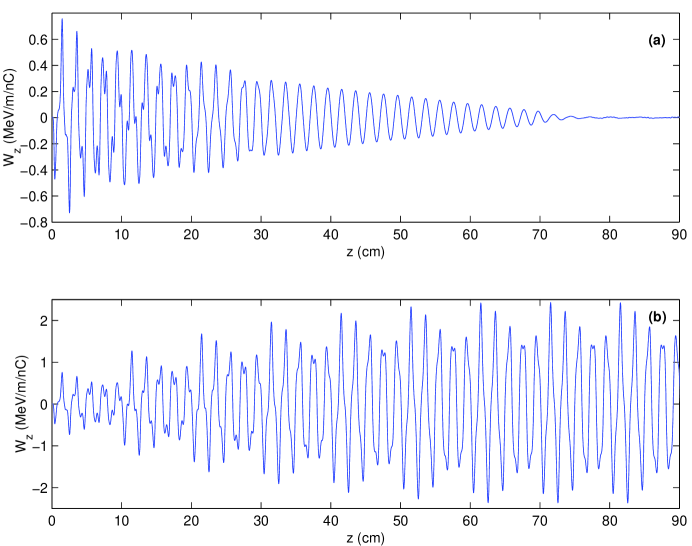
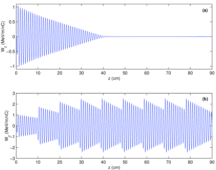
The bunch train wakes shown in figures 2b and 3b reflect finite structure length and group velocity effects by their not purely sinusoidal character. In order to compute the useful power generated at the fundamental, we filter the data by performing an FFT and zeroing all Fourier components outside a fixed window in . The inverse FFT then yields the amplitude W of the wake within that bandwidth, and the power generated is
| (3) |
Table 1 summarizes the parameters of these structures. The power generated is large, on the order of 100 MW for a 30 cm test structure with and scaling quadratically with the length of the device. In the 30 GHz case the dielectric device performance is comparable to the CLIC designs R9 while being easier to manufacture and to incorporate parasitic mode damping.
| Frequency (GHz) | 15 | 30 |
| Charge per bunch (nC) | 10 | 10 |
| Bunch length (mm) | 1 | 1 |
| Bunch spacing (ps) | 333 | 333 |
| Structure length (cm) | 30 | 30 |
| Inner radius (mm) | 5 | 4 |
| Outer radius (mm) | 7.38 | 5 |
| Dielectric constant | 4.5 | 4.5 |
| Loss tangent | 0.0002 | 0.0002 |
| Group velocity | 0.28 | 0.41 |
| Attenuation of the structure (dB) | 0.35 | 0.53 |
| Power generated () (MW) | 94 | 178 |
| Peak deceleration field (MV/m) | 23.6 | 24.3 |
| Normalized shunt impedance (M) | 0.1002 | 0.0516 |
5 Summary
We have presented designs for dielectric power extraction structures for two-beam accelerators which are able to produce power levels competitive with conventional copper structures while at the same time possessing the advantages of ease of construction and straightforward implementation of parasitic mode damping. We plan to build and test a 15 GHz device at our laboratory and if successful build a 30 GHz device for the CLIC test facility.
References
- (1) B. Danly, in Advanced Accelerator Concepts, Fontana, WI 1994, edited by P. Schoessow, AIP Conference Proceedings No. 335 (American Institute of Physics, Woodbury NY 1994)
- (2) G. Loew, J. Wang, SLAC-PUB-7684, (October 1997)
-
(3)
A. Sessler, AIP Conference Proceedings No. 91,
edited by P. Channell (1982)
W. Schnell, CERN-LEP-RF/86-06 - (4) W. Gai et al., Phys. Rev. Lett 61, 2756 (1988)
- (5) P. Schoessow et al., J. Appl. Phys. 84, 663 (1998)
- (6) E. Chojnacki et al., J. Appl. Phys. 69, 6257 (1991)
- (7) Trans-Tech Inc., Catalog No. 5520, Adamstown, MD 21710
- (8) P. Zou et al., to be published in Review of Scientific Instruments
- (9) H. Braun et al., CLIC Note 364 (unpublished)
- (10) M. Rosing, W. Gai, Phys. Rev. D 42, 1829 (1990)
- (11) R. Ruth, private communication
- (12) W. Gai, WF-186 (unpublished). Available as web resource http://www.hep.anl.gov/awa/awa/docs/wf186.pdf.
- (13) P. Schoessow, W. Gai, in Quantum Aspects of Beam Physics, P. Chen ed., World Scientific 1999, p. 289