Test Results on the Silicon Pixel Detector for the TTF-FEL Beam Trajectory Monitor
Abstract
Test measurements on the silicon pixel detector for the beam trajectory monitor at the free electron laser of the TESLA test facility are presented. To determine the electronic noise of detector and read-out and to calibrate the signal amplitude of different pixels the 6 keV photons of the manganese line are used. Two different methods determine the spatial accuracy of the detector: In one setup a laser beam is focused to a straight line and moved across the pixel structure. In the other the detector is scanned using a low-intensity electron beam of an electron microscope. Both methods show that the symmetry axis of the detector defines a straight line within 0.4 m. The sensitivity of the detector to low energy X-rays is measured using a vacuum ultraviolet beam at the synchrotron light source HASYLAB. Additionally, the electron microscope is used to study the radiation hardness of the detector.
keywords:
Beam monitor, X-ray detector, solid-state detector, imaging sensor.PACS:
41.85.Qg, 07.85.Fv, 29.40.Wk, 42.79.Pw.DESY 00-065 physics/0004063
April 2000
, , , , , , , , , , , , ,
1 Introduction
It is a widespread opinion that the fourth generation synchrotron light source will be a X-ray free electron laser (FEL). It will consist of a single-pass FEL relying on the self-amplified spontaneous emission (SASE) mechanism [1] and deliver coherent radiation in the X-ray range with unprecedented brilliance. In such SASE FEL a tightly collimated electron beam of high charge density is sent through a long undulator. The SASE effect results from the interaction of the electron bunch with its own radiation field created by the undulation motion. This interaction can only take place if the electron and the photon beams overlap.
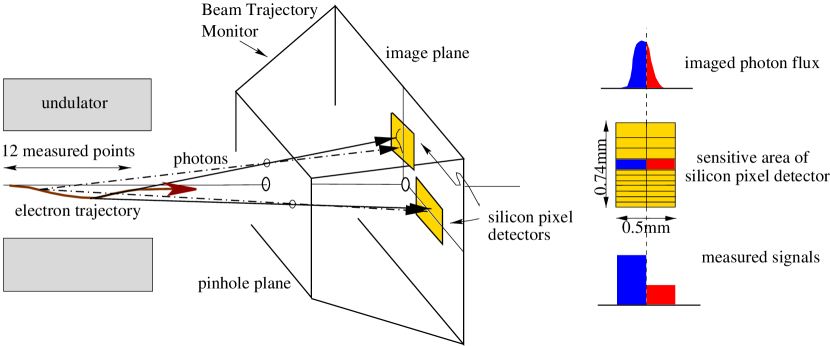
At the free electron laser of the TESLA Test Facility (TTF-FEL) [2] the electron beam position must be controlled to better than 10 m over the entire 15 m long undulator. With the beam trajectory monitor (BTM) [3] the off-axis spontaneous undulator radiation is imaged through a set of pinholes of 80 m diameter (see Fig. 1). In order to reduce the effect of diffraction, only the higher harmonics of the spontaneous undulator radiation will be used for BTM measurements. A 120 nm thick silver foil across each pinhole absorbs all low energy photons and restricts the spectral range of the detected radiation to energies above 100 eV. From a simulation using the expected undulator spectrum the Gaussian width of the photon spot at the position of the detector 0.5 m behind the pinholes is estimated to 30 m. To achieve the required resolution of the BTM, the center of the photon spot will be measured with a precision of better than 1 m using a high resolution silicon pixel detector. It delivers 12 points of the transverse beam position with an accuracy of better than 10 m over a length of 5 m using a single setup. The performance of the silicon detector with respect to noise, spatial precision, radiation hardness and quantum efficiency is presented in this paper.
2 The Silicon Pixel Detector
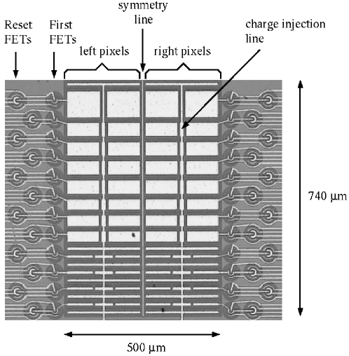
A silicon pixel detector with an active area of 0.5 mm 0.74 mm and a total of 24 channels was designed and fabricated at the MPI Halbleiterlabor. The sensitive area of the detector consists of two rows of each 12 active pixels as shown in Fig. 2. Each pixel anode is directly connected to an on-chip JFET for low noise read-out. The pixels are 250 m wide, with heights varying from 25 m (nearest to beam) to 100 m to give roughly equidistant measuring points in the projection along the undulator axis. High quantum efficiency is achieved using a thin entrance window technology [4].
The concept of a backside illuminated -junction detector has been chosen, which shows not only a high quantum efficiency for the desired photon energies, but in addition an excellent spatial homogeneity. It consists of a fully depleted -type bulk and a non structured -rear contact, acting as radiation entrance window. At photon energies of about 150 eV the absorption length in silicon drops to 40 nm, which leads to signal loss in the almost field free, highly doped region underneath the contact. To reduce the width of this insensitive region the implantation of boron ions was done through a SiO2 layer, which has been removed afterwards. One achieves a shallow doping profile with the -junction placed at a depth of only 30 nm below the detector surface. Ionizing radiation which penetrates through the dead layer generates electron hole pairs in the sensitive volume of the detector. Applying a negative voltage of about 120 V to the rear contact totally depletes the detector and causes the signal electrons to drift towards the collecting pixel anodes (see Fig. 3).
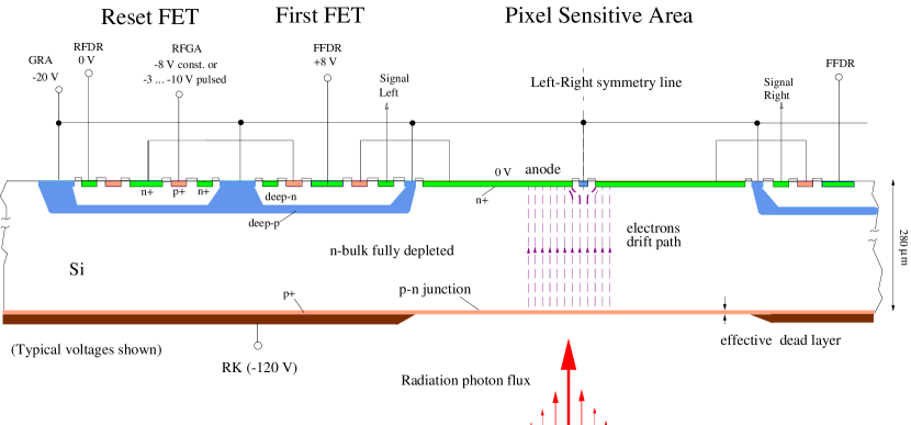
The pixels are formed by -implants and are isolated from each other by a 5 m wide grid. Each pixel anode is connected to an amplifying JFET which is integrated on the detector chip, thus minimizing stray capacitances. The JFETs are operated as source followers with a given constant current of about 200 A from source to drain. The collected signal charge is transferred to the gate and modulates the voltage drop across the JFET. A second JFET (Reset FET) allows to discharge the pixel anodes after each read-out cycle.
The 4 mm 2.5 mm large detector chips are mounted onto a ceramic hybrid board. Each detector pixel is connected to one channel of the CAMEX64B [5] read-out chip. It provides signal amplification, base line subtraction, and multiplexed output. The digital steering chip TIMEX generates the necessary control signals. Signal integration times between 2 s and the full TTF pulse length (800 s) can be programmed.
3 Calibration and Noise Determination
An absolute energy calibration of each detector pixel is obtained using mono-energetic photons emitted from a 55Fe source at 5.90 keV (Mn Kα-line, 89.5%) and 6.49 keV (Mn Kβ-line, 10.5%). The X-ray photons enter the detector through the back entrance window on the side opposite to the anodes. Photons at an energy of 6 keV have an attenuation length of 30 m in silicon and are therefore absorbed close to the surface of the detector chip. On average each photon at this energy produces about 1600 electron-hole pairs. The electrons drift to the anodes, where the charge is collected. During the drift time of 7 ns the lateral extent of the electron cloud increases to about 8 m due to diffusion.
The detector is operated at room temperature and read out with a rate of 5 kHz. For the given activity of the source ( Bq) and the integration time (15 s) a photon is registered by the detector in 10% of the read-outs. The measured energy spectrum for one of the detector pixels is shown in Fig. 4.
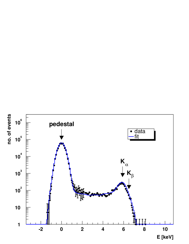
It can be separated into three parts: The pedestal peak, which dominates the distribution, the signal peak, which consists of the Kα and Kβ components, and the region in between, which is caused by charge sharing between adjacent pixels. The energy scale, the noise and the diffusion width are determined with a simultaneous fit to the whole spectrum of Fig. 4 based on a model describing the two-dimensional pixel structure.
The location of the pedestal defines the zero-signal level for each pixel. The pedestal subtraction has already been applied to the data shown in Fig. 4. The difference between the signal and pedestal peak gives an energy calibration for each pixel. The resulting calibration constants differ by at most 10% for neighbouring left and right pixels. For a 30 m photon spot this corresponds to an error in position reconstruction of at most 0.8 m if the signal is not corrected according to the different calibration constants.
The Gaussian width of the pedestal peak is mainly caused by one source of noise, the leakage current. Using the calibration one calculates energy resolutions between 222 eV and 391 eV, which can be translated into an equivalent noise charge (ENC) between 60 and 106 electrons. The variation of the noise values are caused by the different pixel sizes which lead to variable leakage current and capacitance. Due to the dominant role of the leakage current the energy resolution strongly depends on integration time and temperature. Our measurements show that the noise grows proportionally to the square root of the integration time and decreases by a factor of two when cooling the detector by 16 K.
The number of events with charge division between pixels compared to the number of events with the photon signal fully recorded by one pixel is directly related to the geometry of the individual pixels and the diffusion width of the charge cloud. This is taken into account by the fit and leads to a Gaussian width of the charge cloud at the anode plane of about 8 m, consistent with our estimations from diffusion.
The common mode noise is defined as the variation of the zero-signal level common to all pixels. For each event the median of the 24 pixel signals is taken as an estimate for the common mode value. It has been found that the common mode shows no systematic drift and varies only within its standard deviation of 30 electrons. Electronic cross talk is seen by the pedestal shift of a pixel adjacent to a pixel which registered one photon totally. The cross talk amounts to 3% of the full signal at most. This corresponds to a reduction in spatial resolution by 6% which is acceptable for our application.
4 Measurement of Spatial Accuracy using a Laser Light Spot
The spatial accuracy of the pixel detector is measured in a laser test stand [6] by projecting a laser line-focus onto the pixel structure. The light emitted by a pulsed laser diode ( nm) is focused using a micro-focus lens and then defocused in one plane using a cylindrical lens. This setup produces a straight line-focus of about 30 m full width on the detector surface. The line-shaped light spot is oriented parallel to the separation line of the two pixel rows. Using a stepping device the light spot is moved across the two pixel rows with 0.068 m per step to determine its left-right symmetry line.
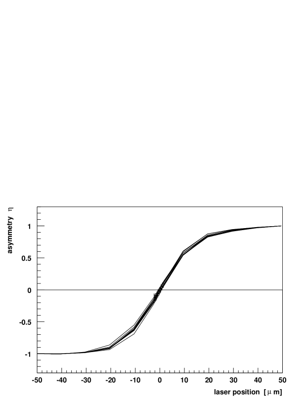
In addition to the pedestal correction we subtract a constant signal offset proportional to the pixel size to correct for stray light falling onto the detector. For each pixel pair the relative difference between the signals of the right and the left pixel, , is calculated. The result is shown in Fig. 5 versus the position of the laser light spot. All 12 pixel pairs show the zero crossing of at the same laser position within m.
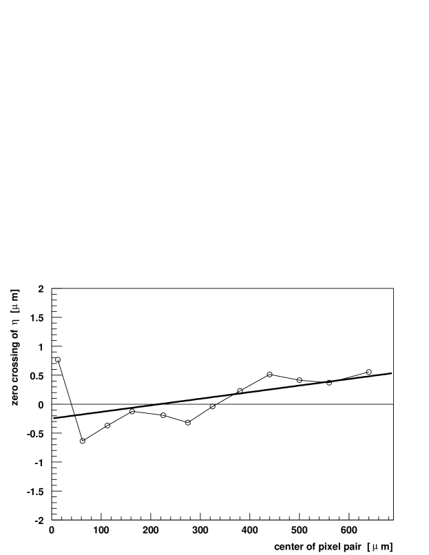
The position of the zero crossing of can be extracted for each pixel pair from a straight line fit to the central data points. In Fig. 6 the resulting zero crossing is plotted versus the center position of the corresponding pixel pair. Obviously, the laser line-focus was tilted by about 1 mrad with respect to the center line of the pixel array. Fitting a straight line to the 12 data points gives us the location of the laser spot. The individual measurements scatter with a standard deviation of 0.37 m around the reconstructed line.
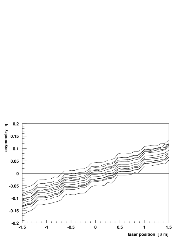
For measurements very close to the zero crossing one expects a linear dependence of on the laser position. Fig. 7 shows the behaviour of the measured in this region. All 12 pixel pairs show the same dependence with the exception of different offsets. We observe a periodic oscillation of 0.5 m length which is caused by the inaccuracy of the stepping device. As these oscillations are fully correlated one can correct for the effect and is left with a relative point-to-point resolution of approximately 0.1 m.
5 Measurement of Spatial Accuracy using a Scanning Electron Microscope
The detector is installed into the focal plane of a scanning electron microscope (SEM). The SEM produces an electron beam with an energy of 10 keV focused to a spot smaller than 1 m on the surface of the detector. The SEM beam current can be adjusted up to 100 A at the filament cathode. It is significantly reduced by several apertures in the optical system, yielding currents below 1 pA at the beam focus. Secondary emitted electrons from the detector surface are collected and amplified by an open multiplier tube. Its signal is used to display a picture of the detector on a view screen. The detector hybrid is placed onto a copper plate to remove the heat produced by the read-out electronics. However, the temperature of the detector chips increases by about 15 K while the chamber is under vacuum.
The electron beam is scanned across the two pixel rows in parallel to their separation line. After each scanning line, the electron beam is displaced by a fixed amount. The detector read-out is synchronized to the scanning frequency of the SEM, so that data are taken after each scanned line. Measurements are made with 618 to 2252 lines per mm.
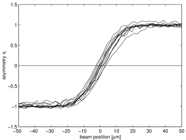
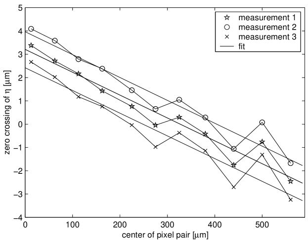
Analogous to the previous measurement the relative asymmetry between right and left pixels is calculated (see Fig. 8) and the zero crossings of are extracted. Fitting a straight line to the central data points gives again the zero crossings for the different pixel pairs. The results of three different scans are shown in Fig. 9. The scanning line of the electron beam was tilted with respect to the symmetry line of the pixel detector by 10 mrad. The standard deviation of the measured zero crossings from the reconstructed scanning line amounts to 0.47 m. The reconstructed scanning lines from three different measurements show the same structure and are only shifted with respect to each other. One concludes that the deviations of the measured zero crossings from a straight line and therefore the limitation in spatial accuracy of the detector is due to a systematic effect. The reconstructed symmetry line cannot be directly compared to the laser measurement of Section 4, because the penetration depth of the electrons is much smaller than for laser light. Additionally, the detector chip was different from the one used in the laser test.
6 Sensitivity to Vacuum Ultraviolet Radiation
We measured the sensitivity of the detector to vacuum ultraviolet (VUV) at the synchrotron radiation facility HASYLAB. For this purpose the detector is illuminated with VUV radiation in the energy range between 50 eV and 1000 eV which is produced by a bending magnet of the electron storage ring DORIS. The hybrid containing the silicon pixel detector and its read-out electronics is placed into the vacuum chamber of a reflectometer, where ultra high vacuum ( mbar) had to be established. The mono-energetic photon beam coming from the monochromator is focused onto the center of the pixel detector. The synchrotron light is pulsed with the 5 MHz bunch frequency of DORIS. The separation of 200 ns between two light pulses is much shorter than the integration time of the detector read-out. Therefore the pixel anodes are discharged at the beginning of each integration period which is extended over several synchrotron light pulses.
The silicon detector response was corrected to the photo-electron emission of one of the focusing mirrors and to a GaAs photo diode as a reference. Using the normalized signals, the quantum efficiency can be estimated from the measured absorption edges of the relevant elements. Detailed measurements were done at photon energies in the vicinity of the absorption edges of silicon (100 eV), oxygen (543 eV), and carbon (284 eV). For the parameterization of the absorption edges the compilation of photon absorption lengths for different elements in Ref. [7] is used. For simplicity we assume that a photon absorbed in the dead layer of the detector does not contribute to the signal and all other photons are fully registered. Using the measured heights of the absorption edges, this model gives the thicknesses of the photon absorbing layers. These are used to calculate the quantum efficiency in the whole spectral range from 50 eV to 1000 eV. The data points are normalized to this result and both are presented in Fig. 10.
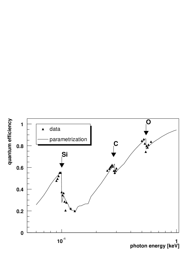
The observed quantum efficiency is explained by the following effects: The electrical field of the detector diode does not extend up to the cathode plane, but leaves space for a dead layer with a thickness of the order of 30 nm, which has to be penetrated by the photons before they enter the sensitive region of the detector. A 50 nm thin passivation layer of silicon oxide on top of the back entrance window leads to further absorption of photons. From a detailed investigation of the silicon absorption edge one can see the effect of the covalent Si-O bond which results in a deviation from the absorption edge of pure silicon (see Fig. 11). The origin of an additional carbon contamination which leads to the appearance of the carbon absorption edge in Fig. 10 is not yet understood.
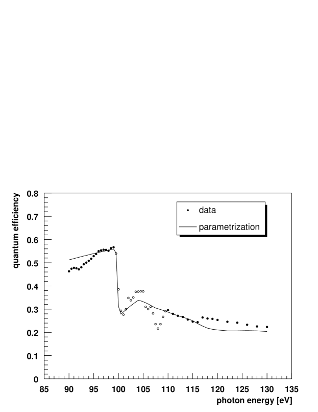
The quantum efficiency of the detector is larger than 20% for photons in the energy range above 100 eV which will be used by the BTM. Absolute measurements with a similar type of detector have been done using a reference diode with known quantum efficiency [4]. The measured quantum efficiencies are comparable with our results, but did not show the problem of the carbon absorption edge.
7 Study of Radiation Hardness
In the BTM the silicon detector will be operated at a distance of only 5 mm from the electron beam of the TTF linac. It can suffer from radiation damages caused by a beam halo or by scraping a misaligned beam. One expects that the radiation damages of the silicon detectors are dominated by surface effects.
Placing the silicon detector inside an electron microscope not only allows to determine its spatial accuracy, but also gives the opportunity to study radiation hardness against surface damages. The detector side containing the pixel anodes and the amplifier JFETs should be more sensitive to surface damages than the back entrance window. Therefore we place the detector in such way that the electrons enter the detector opposite to the entrance window. One of the two pixel rows, including its JFETs, is irradiated using the 10 kV electron beam with beam currents of the order of several tens of pA. Irradiation takes place with all operating voltages on, including the bias voltage.
Before irradiation the detector had been calibrated using the 59.5 keV photons of an 241Am source. During the irradiation procedure, the beam scan is extended to all pixels and the detector is read out. This is done to determine the number of incident beam electrons from the measured signal of the undamaged pixels. From the mean energy loss of a 10 keV electron in silicon oxide (4.13 keV/m) one can then calculate the radiation dose. Typical dose rates between 0.1 Gy/min and 10 Gy/min have been achieved with this method. The measurement of the beam current was cross checked using a faraday cup which delivered consistent results within 20%.
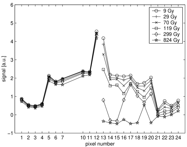
Several data sets are taken in between the irradiation steps to determine the change of signal height and noise level. For this purpose a LED is installed inside the electron microscope shining onto the back entrance window of the silicon detector. Fig. 12 gives the measured signal height versus the pixel number, starting from the small left pixels (1–4), going to the large pixels (12,13) and ending with the small right pixels (21–24). The irradiated pixels on the right side show a decreasing signal height with increasing radiation dose. Above radiation doses of about 300 Gy some of the irradiated pixels cease to deliver any signal at all.
In Fig. 13 the dependence of noise on the radiation dose is shown. One can clearly distinguish between the non-irradiated pixels and the irradiated ones. Whereas the first stayed at the same noise level the equivalent noise charge of the latter increased by a factor of three after a total radiation dose of 120 Gy.
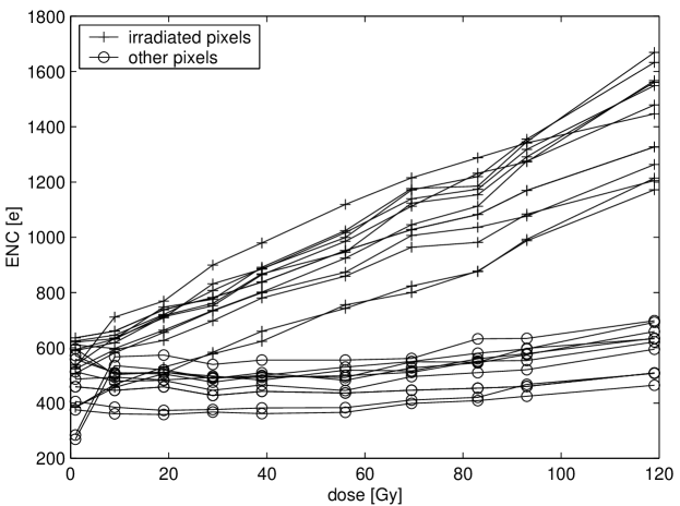
Surface damages include both the creation of oxide charges in the passivation layer and the generation of inter-band energy levels at the interface between the silicon bulk and the oxide layer, the so-called interface states. The latter inject additional charges and therefore contribute to leakage current and noise. The oxide charges lead to a charge up of the SiO2 layer and therefore influence the operating voltages of the integrated JFETs. The signal loss with increasing radiation dose might be caused by a change of the operation point of the amplifying JFET which results in a lower gain. In addition to the amplifying JFET each pixel is connected to a reset JFET which allows discharging the pixel anode between detector read-outs. By recording the dependence of the amplified signal on the applied gate potential, we measured the gate potential which was necessary to close the reset FET. This voltage had to be increased from V to V after a irradiation of 120 Gy.
Further irradiations up to 0.8 kGy were performed, which caused the loss of signal in all irradiated pixels. Recovery of the pixels took place within one week (165 h). Then the total radiation dose was increased to 4 kGy. This time the detector could not recover within the following week. After an in-situ heating of the detector and the read-out electronics to 130 ∘C for 30 minutes all pixels worked again. The effect can be explained by the removal of the oxide charges due to the heating process. Because the interface states cannot be removed by heating the noise stayed at a high level, a factor of two above the noise of the non-irradiated pixels.
8 Conclusions
Noise, spatial accuracy and quantum efficiency of the silicon pixel detector which will be used in the beam trajectory monitor at TTF-FEL were investigated. The measured noise values are in the specified range and are dominated by leakage current. The systematics of the position measurement was studied using a laser line-focus and a scanning electron microscope. The spatial accuracy is of the order of 0.4 m, well below the required 1 m for the operation within the beam trajectory monitor. The sensitivity to vacuum ultraviolet radiation has been measured in a synchrotron beam line. From the observed absorption edges a quantum efficiency above 20 % is estimated at photon energies used for the BTM. The detector can cope with radiation doses up to 100 Gy. At the position of the BTM in TTF a radiation dose of the order of 1 Gy per week is expected.
References
-
[1]
A. M. Kondratenko, E. L. Saldin,
Part. Accelerators 10 (1980) 207;
R. Bonifacio, C. Pellegrini, L. M. Narducci, Opt. Commun. 53 (1985) 197. -
[2]
TTF-FEL Conceptual Design Report,
TESLA-FEL 95-03, DESY, June 1995;
J. Rossbach et al., Nucl. Instr. and Meth. A375 (1996) 269. -
[3]
J. S. T. Ng, TESLA-FEL 96-16, DESY, 1996;
AIP Conf. Proc. #413, eds R. Bonifacio and W. A. Barletta, 1997;
J. S. T. Ng et al., Nucl. Instr. and Meth. A439 (2000) 601. -
[4]
P. Lechner, L. Strüder,
Nucl. Instr. and Meth. A354 (1995) 464;
R. Hartmann et al., Nucl. Instr. and Meth. A377 (1996) 191;
H. Soltau et al., Nucl. Instr. and Meth. A377 (1996) 340. - [5] W. Buttler et al., Nucl. Instr. and Meth. A288 (1990) 140.
- [6] S. Hillert, Diploma-Thesis Univ. of Hamburg, TESLA 2000-04, DESY, Jan. 2000.
- [7] B. L. Henke, E. M. Gullikson, J. C. Davis, Atomic Data and Nuclear Data Tables 54 (1993) 181 and http://cindy.lbl.gov/optical_constants.