Mechanisms of spatial current-density instabilities in ---- structures
Abstract
Semiconductor ---- structures with large junction and contact areas are treated as 12-dimensional active media, in which self-organized pattern formation can be expected. The local bistable behavior of the structures may emanate from two different mechanisms both governed by a nonlinear current feedback-loop between the electrons and holes injected from the outer layers. By considering the device to be composed of an active subsystem with negative differential resistance and a passive resistive layer with positive differential resistance an analytical approach is suggested to understand and describe the corresponding physical mechanisms in a self-consistent way. Analytical solutions of the derived model equations allow a description of homogeneous stationary states and yield explicit expressions of the current-density vs. voltage characteristics of the whole structure and its subsystems. A stability analysis of the homogeneous states with respect to two-dimensional transversal harmonic fluctuations is performed for the two cases under study. The resulting dispersion relations allow two different types of instability. While the first one is of Ridley’s type which is characteristic for any spatially extended electrical system with negative differential resistance, the second type can be considered as a solid-state analogue of Turing’s instability known as a generic instability mechanism which may lead, e. g., to the formation of periodic patterns.
I Introduction
Basic ideas on instabilities and dissipative pattern formation in open spatially extended nonlinear systems [1, 2, 3] have gained substantial interest in many fields of science in the last two decades. (see, e. g., Refs. [4, 5, 7, 6, 8]). The investigations become rather intensive also in the field of solid-state physics and electronics [4, 9, 10] where a large variety of different nonlinear nonequilibrium phenomena occurs, which can cause spontaneously arising spatio-temporal patterns in materials and devices. Together with highly developed device technology, these circumstances suggest promising opportunities for future research and developements.
Recently, attention has been called to thyristor-like semiconductor structures with large active areas [11, 12, 13, 14], as these nonlinear systems with bistable properties show several spatial and spatio-temporal current-density patterns. Such semiconductor structures could potentially be used as multi-stable elements for integrated circuits, self-organizing devices for image recognition and image processing, etc. [3, 15, 16]. One of the most striking results of former considerations based on phenomenological models [11, 13] is that the instability mechanisms posess some features very similar to those studied in biology or chemical media, which may show an extremly manifold selforganizing behavior. However, at present the understanding of instability mechanisms and pattern formation in multilayer structures is far from being complete. Apparently, there is a lack of systematic investigations concerning self-organization aspects for this family of devices. In a very early theoretical paper [17] the process of single current filament formation has only been analyzed for the simplest case of --- structures, that according to Ridley’s terminology [18] belong to the class of extended electrical systems with current controlled negative differential resistance. Recently, gate-driven --- structures have been used to study current filamentation and the dynamics of switching fronts under the constraints of two global couplings [19, 20]. In specially designed multilayer structures different types of filament oscillation have been observed [21, 22, 23]. Very few theoretical papers have been devoted to instabilities in standard thyristors; they all aimed merely on a safe operation in power applications [24, 25, 26]. Furthermore, it is not an easy task to adapt the advanced experience of power device technology directly to the specifics of devices showing phenomena of self-organization. One of the main reasons for this is that the operation of semiconductor devices and especially thyristors depends very sensitively on many physical and design parameters. On the one hand, this gives numerous opportunities for a proper choice of those parameters responsible for the intended function of these devices. But on the other hand the high-dimensional parameter space makes a systematic analysis rather difficult, because the use of numerical methods and the performance of experiments are usually time-consuming and/or expensive. Therefore detailed studies of the underlying physical processes in conjunction with the material and the design parameters are necessary and should lead to the deepest possible analytical description of the device physics.
Following this motivation and aiming at further development of concepts introduced earlier in Refs. [11, 27, 14] we suggest in this paper an analytical approach for instability mechanisms in a family of devices based on thyristor-like ---- structures, in which several modes of pattern formation have already been found experimentally [11].
The outline of the paper is as follows: In section 2 the investigated semiconductor structure and its basic physics with emphasis on the nonlinear properties are described. A non-stationary 12-dimensional model rendering possible an analytical investigation of two-dimensional current-density and potential distributions transversal to the main current flow direction is derived in section 3 for two cases characterized by different nonlinear electrical mechanisms. In section 4, stationary homogeneous states are determined from the model equations and used to derive the current-voltage characteristics for systems with uniform current-density distributions. Finally, the stability of stationary homogeneous states is studied in section 5, including a discussion of important parameter dependencies.
II Multilayer semiconductor structures as 12-dimensional extended active media
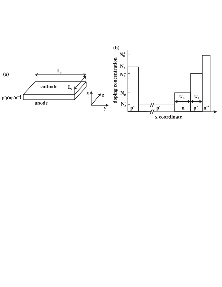
The system under consideration consists of a semiconductor structure with a vertical width of several hundreds of m and with the two other (transversal) widths . Along the vertical direction the structure is characterized by a ---- doping profile as schematically shown in Fig. 1. The outer and layer of the structure are provided with metal contacts. The internal design of the structure possesses the following peculiarities:
(i) Along the (vertical) -direction the ---- structure can be divided into an active (triggering) subsystem consisting of a four-layer thyristor-like --- structure and a subsystem of a distributed resistive layer consisting essentially of the remainder layer. Note that the thyristor-like regeneration mechanism in the active subsystem causes an autocatalytic increase of the current density in a certain current interval which is counteracted by the resistive layer.
The width of the -- part is only a few tens of m which is more than an order less than the whole width of the device. The lifetime of the excess carriers in the bulk material is supposed to be so small that conductivity modulation of the bulk due to the injection of electrons and holes from the outer and layers is prevented. This can be achieved by reducing the lifetime in the main part of the bulk in a certain distance to the anode contact leaving a relatively thin part of the layer with large nearby the inner layer.
(ii) The doping concentrations and in the layers forming the cathode emitter - junction [Fig. 1(b)] are similar to those used in high frequency bipolar transistors. The electron injection efficiency of this junction increases from nearly zero at very low current densities to a saturation value of approximately 0.8-0.9 at rather small current densities of the order of 1 mA/cm2.
(iii) The doping concentration of the layer is much smaller than the doping concentration of the base. Hence, for low currents, current transport through this junction is dominated by a leakage current of electrons from the base into the emitter and, consequently, the injection efficiency of the - junction is very small.
(iv) The widths of the and base, and , in the thyristor-like subsystem are much smaller than the diffusion lengths and of the minority carriers in these layers: , . Consequently, both base transport factors are about one.
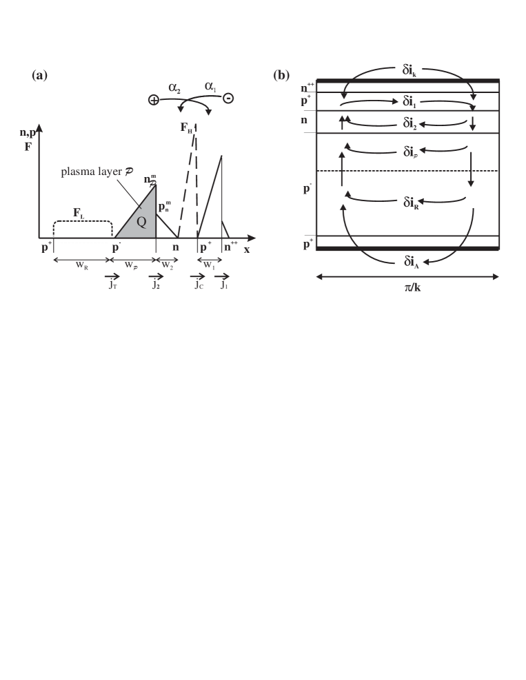
When a dc voltage is applied to the device such that the outer layer is biased negatively with respect to the outer layer, the anode and cathode emitter junction are forward biased, while the collector junction is reverse-biased. Thus, double injection occurs inside the thyristor-like subsystem accompanied by a characteristic nonequilibrium plasma-field stratification along the vertical direction as shown in Fig. 2(a). Due to the chosen doping proportion at the - junction, which is just inverse to that in standard thyristors, there is a significant electron leakage current from the base into the layer which obviously exceeds the electron injection current. Therefore, a rather large excess charge accumulates in a thin plasma layer ( layer). If the carrier lifetime in this plasma layer is sufficiently large, the local dynamics of this charge at non-stationary conditions may be considered to be the most inertial process, thus determining the temporal evolution of the whole device. The derivation of the model equations in section 3 is based essentially on these physical properties.
The nonlinear feedback mechanism between the electron and hole injection currents in the --- subsystem is similar to that in standard thyristors. However, there are remarkable peculiarities and it is useful to distinguish between two cases, corresponding to certain current intervals, which are characterized by a particular nonlinear mechanism, respectively, causing the appearance of negative differential resistance in the current-voltage characteristic of the thyristor-like subsystem. In analogy to the two-transistor approach for thyristors we consider the thyristor-like subsystem to be composed of an -- and a -- transistor to specify the two different regenerative mechanisms. Current regeneration [28, 29] in thyristors is possible for current intervals, in which the condition holds, where and denote the thyristor voltage and current, and is the differential resistance. is implicitly given by the steady state condition
| (1) |
where and denote the current gains of the -- and the -- transistor, respectively [Fig. 2(a)].
Charge carrier recombination in the space charge region of the emitter junction of a transistor influences the current gain significantly [28, 29] and typically leads to a monotonic increase of the current gain with increasing current for not too large currents.
Consider the device parameters to be of such kind that the current gain approaches a value close to one at relatively low currents (A/cm2). Then Eq. (1) can be fulfilled at a very low injection efficiency of the - emitter junction. Thus, this case – subsequently called low current range – is roughly characterized by and .
If the doping profile and other parameters are chosen such that saturates in the low current range before Eq. (1) is true, regeneration does not occur at low currents. Nevertheless, at larger currents regeneration might become possible again when increases monotonously with the current. This can occur at sufficiently large current, when a plasma layer evolves in the layer near the - junction and the injection of excess holes from this plasma layer into the base increases superlinearly as proposed by Fletcher [30]. Consequently, the layer plays the role of a plasma emitter, the efficiency of which rises strongly with the current so that Eq. (1) can be fulfilled. This case is called moderate current range subsequently and is roughly characterized by and .
Before we start with a detailed analysis of these two cases let us turn to a short discussion on important transversal processes which have to be taken into account for an analytic description, too. To this end, consider a so-called differential element of the whole ---- structure, which is small in and direction. Fig. 2(b) shows schematically contours of possible current fluctuations in such an element which may lead to a destabilization of the homogeneous current flow. Obviously, there are three channels along which transversal currents effect a transversal spatial coupling in the thyristor-like subsystem: the base, the base, and the possibly conductivity modulated layer in the bulk, in which the corresponding transversal fluctuations , , and may arise. For the resistor subsystem transversal current fluctuations are taken into account; they are distributed over the whole bulk due to three-dimensional deformations of the potential distribution ; these deformations are caused by potential fluctuations at the interface between the two subsystems, which in turn result from local current fluctuations in the thyristor-like subsystem.
The metallic layers forming the anode and cathode contact on the top and bottom of the device represent further channels denoted by and in Fig. 2(b) and render possible the formation of closed loops of current fluctuations inside the system without any interaction with elements of the external circuit. Thus, all differential elements of the system are connected to each other by both the vertical feedback mechanism and transversal couplings which have to be considered in a self-consistent description as outlined in detail in the following sections.
III Non-stationary (12)-dimensional analytical model
A The thyristor-like subsystem
As mentioned above the excess plasma of the layer is considered to be the most inertial part of the system. Consequently, all other nonstationary transport effects are neglected. We start with a derivation of the basic equations for the low current range. Based on these results the peculiarities concerning the case of moderate currents are discussed in a second subsection.
1 Low current range
In the low current case the dynamics of the plasma emitter can be described in terms of the excess charge density per unit square in the plasma layer :
| (2) |
where
| (3) |
is the sheet electron current-density in the plasma layer, the two-dimensional -operator, the diffusion coefficient of electrons, the lifetime of excess charge carriers at low injection, the component of the electron current-density at the boundary between the plasma layer and the base, the component of the electron current-density leaving the thyristor-like subsystem and entering the resistor subsystem.***Note that all quantities denoted by refer to the component of the corresponding current-density vector; for a better readability the supplement component is omitted in the following explanation. Accordingly, quantities denoted by refer to pure sheet current densities per unit length in a certain layer of the structure. Physical constants as well as material and design parameters are listed separately in Tables I and II. denotes the voltage drop across the thyristor-like subsystem, the acceptor concentration of the layer, the conductivity of the plasma layer , which is equal to in the low current range, the elementary charge, , and the electron and hole mobility, and the average electron density per unit square in the plasma layer with width .
Following the charge-control model of transistors and thyristors (see, e.g., Ref. [28]) the variable can be expressed by
| (4) |
Thus, the charge equation can be re-written as
| (5) |
with . The variable can be further approximated in the following way by means of the maximum value of the excess charge carrier concentration in the plasma layer:
| (6) |
Relations connecting the concentrations of the minority charge carriers at both sides of the - junction, and , and the hole current-density at the interface between the plasma layer and the base are provided by the classical theory of - junctions (see, e. g., Ref. [29]):
| (7) | |||||
| (8) |
where is the donor concentration in the base, the effective width of the base, which depends on the voltage drop across the - collector junction, and the diffusion coefficient of holes. Note that due to the assumption [Sect. 2, assumption (iv)] the hole current-density at the collector is equal to .
The dependence of the base width on the collector voltage drop can be approximated by (see Ref. [29]):
| (9) | |||||
| (10) |
where denotes the whole width of the base, the punch-through voltage of the - junction, and the vacuum permittivity and the dielectric constant of silicon.
Equations (6) - (8) yield an expression linking the hole current-density at the collector junction, , the charge and the collector voltage :
| (11) | |||||
| (12) |
In the -- transistor the local current balance for a differential element of the base is given by:
| (13) | |||||
| (14) |
where and denote the total current-densities at the - collector and - emitter junction, the conductivity of the base, and the voltage drop across the emitter junction.
Because of , the electron current-density at the collector is practically equal to the electron current-density injected by the layer. Nevertheless, since the hole leakage from the base into the emitter is strongly nonlinear we have to take into account a -dependence (or bias-dependence) of the parameter . The parametric dependence between the total emitter current-density and its electron injection component is given as an implicit function coupling the emitter voltage with the emitter current-density :
| (15) | |||||
| (16) |
Here , and are saturation values of the electron injection current-density, and the linear and nonlinear hole leakage current-densities, respectively. The parameter depends on the concrete mechanism of the hole leakage in the - junction [14]. For the case under study we assume , i. e. Sah-Noyce-Shockley recombination in the space charge region.
In the -- transistor the local current balance for a differential element of the base and of the plasma layer is given by:
| (17) | |||||
| (18) | |||||
| (19) | |||||
| (20) | |||||
| (21) |
where is the conductivity of the base. Note, that low injection conditions are assumed for the plasma emitter.
The voltage drop across the thyristor-like subsystem is given by , where is the voltage drop across the - junction. Using and Eqs. (6) and (7) the following relation between and can be derived:
| (26) | |||||
| (27) |
where and denote the equilibrium minority carrier concentrations of the base and bulk, respectively, and is the intrinsic carrier concentration.
2 Moderate current range
Now we indicate the peculiarities occuring at moderate currents, which case is characterized by a high injection level in the bulk. In this case ambipolar effects in the plasma layer should be included into consideration. In the frame of the charge-control model the following relations between the current densities and , the sheet current densities and and the charge in the plasma layer are valid:
| (28) | |||||
| (29) | |||||
| (30) |
Here is the transversal conductance of the plasma layer, the transit time through the plasma layer, and the ambipolar diffusion coefficient. Note that Eqs. (28) and (30) substitute Eqs. (4) and (3), respectively.
The charge balance equation for the plasma layer should be re-written as
| (31) |
where is the high-injection lifetime. By inserting Eqs. (28) and (30) we obtain
| (32) |
[compare with Eq. (5)].
The relation between the excess carrier concentrations at the borders of the space charge region of the - junction changes from Shockley’s to Fletcher’s [30] form:
| (33) |
[compare with Eq. (7)].
Taking into account Eqs. (6), (8), and (33) we obtain in analogy to Eq. (11) an expression linking the charge in the plasma layer, the voltage drop across the --- subsystem and the hole current-density of the collector:
| (34) |
where the normalizing quantities and are connected by
| (35) |
As already mentioned above, the current gain of the -- transistor is approximately current-independent in the moderate current range. Then, the electron current-density of the collector is given by
| (36) |
In the -- transistor conductivity modulation in the plasma layer due to excess carrier concentrations should be taken into account at high injection level; consequently Eq. (21) is substituted by:
| (37) | |||||
| (38) |
On account of vanishing field and diffusion currents at the transversal borders of the sample () the following boundary conditions for the --- subsystem have been chosen for both the low-injection and the high-injection case:
| (39) | |||||
| (40) | |||||
| (41) | |||||
| (42) |
Here is a unit vector normal to the transversal surfaces of the sample.
B Resistor-like subsystem and external circuit
In the resistor-like part of the bulk displacement currents are neglected. The three-dimensional potential distribution in this region is described by Laplace’s equation:
| (43) |
with the boundary conditions
| (44) | |||
| (45) |
where denotes the voltage drop across the whole sample, the width of the resistive layer, and the three-dimensional Laplace-operator.
The current-density vector inside the bulk is connected with the local potential according to
| (46) |
and its component at the boundary ”feeds” the thyristor-like subsystem locally so that
| (47) |
The ---- sample is driven by an ideal voltage source via an external load resistor . This yields the following load line equation:
| (48) |
IV Homogeneous stationary states and corresponding current-density vs. voltage characteristics
To describe the homogeneous stationary states Eqs. (5), (13), (19), (24), and (43) for the low current range and Eqs. (13), (19), (32), (38), and (43) for the moderate current range with all time and space derivatives set to zero have to be solved: . This leads to .
A Low current range
The current gain of the -- transistor can be written as
| (49) |
Combining the charge balance equation (5) for the stationary homogeneous state with and Eq. (49) yields
| (50) |
According to Eq. (11) the variable is proportional to , which is equal to ; together with Eq. (9) and one obtains:
| (51) |
Combining Eqs. (50) and (51) leads to the following parametrically determined -characteristic of the thyristor-like --- subsystem for the low current range:
| (52) |
where the voltage drop across the - emitter and the current density are coupled by
| (53) |
The differential resistance of the thyristor-like subsystem for the homogeneous state under low current conditions is then given by:
| (54) | |||||
| (55) |
B Moderate current range
Using the charge balance equation (32) and we obtain the following relation between and :
| (56) | |||||
| (57) |
On the other hand, for the homogeneous case the variable depends on according to the relation
| (58) |
Choosing
| (59) |
and equalizing Eqs. (56) and (58) yields together with Eq. (35) the following expression for the -characteristic of the thyristor-like subsystem for the case of moderate currents:
| (60) |
The specific differential resistance of the thyristor-like subsystem in the homogeneous state for this case is:
| (62) | |||||
| (63) |
C The global current-density vs. voltage characteristic
The global -characteristic of the complete ---- structure ensues from
| (64) |
where denotes the voltage drop across the resistive layer, the resistance of which is determined by .
D Calculated current-density vs. voltage characteristics
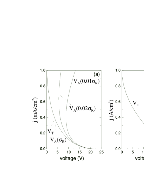
By properly adjusting the design parameters of the layer it is possible to realize the appearance of a negative differential resistance for both the low and moderate current case. In the calculations presented below the saturation current-densities and have been used to adjust the two cases. Figure 3(a) shows stationary current-density vs. voltage characteristics for the low current case. Besides the characteristic of the thyristor-like subsystem and the characteristic of the total structure , which are both calculated for the set of standard parameters, two further -characteristics for reduced values of the conductivity of the bulk are plotted. For standard parameter values the bulk resistance of the bulk is not sufficiently large to compensate the negative differential resistance of the thyristor-like subsystem at low currents. For this reason the two curves and are nearly identical and cannot be distinguished in the diagram. In fact, the current-density , at which the negative differential resistance transforms to a positive one, are nearly equal and approximately 1 mA/cm2 for the two cases. can be reduced by a considerable amount only, if the resistance of the bulk is enlarged at least by a factor of ten, as illustrated by the two other curves in Fig. 3(a).
Figure 3(b) shows current-density vs. voltage characteristics for the case of moderate currents and the standard value of the conductivity of the bulk. The current-density , at which the differential resistance changes from negative to positive values, is 0.45 A/cm2 for the total structure, i. e. considerably lower than the corresponding value ( 1 A/cm2) for the thyristor-like subsystem.
The blocking voltage is approximately equal to the punch-through voltage for both the low and moderate current case. This is because the emitter efficiencies are very small at low currents, so that a hole injection current from the anode emitter, that is sufficiently large to initiate the regenerative process, becomes possible only, when the effective width of the base is approximately zero, i. e. under punch-through condition.
V Transversal stability analysis
In this section we analyze the stability of stationary homogeneous states along the transversal dimensions with respect to small 12-dimensional fluctuations of the space-dependent variables . The standard approach for the linearization procedure implies to make the following Ansatz for all variables in the vicinity of a stationary state
| (65) |
The small variations introduced here have to satisfy the same boundary conditions as the variables [see Eqs. (39)-(42) and (44), (45)].
A Fluctuations of the potential in the resistive layer
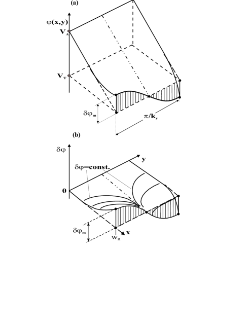
The distribution of the potential in the resistive layer, which is essentially three-dimensional, can be described as solution of the Laplace equation (43) with the boundary conditions (44) and (45). A general solution of this equation is a superposition of a uniform excitation mode and various -modes describing spatially periodic potential perturbations:
| (66) |
with , , and denoting integers. Figure 4 illustrates the potential fluctuations as well as the potential in a reduced two-dimensional space. For a given potential fluctuation at the boundary between the resistive layer and the thyristor-like subsystem the -dependence of the potential variations in the resistive layer is given by:
| (67) |
The component of the current density at the border between the thyristor-like subsystem and the resistive layer is equal to the local anode current-density of the thyristor-like subsystem [see Eqs. (46), (47)], so that the following relation is valid:
| (68) |
From Eqs. (67) and (68) one obtains the following variational derivative by which fluctuctions of and are coupled for each wave-number :
| (69) | |||||
| (70) |
The quantity can be considered as an effective specific resistance of the bulk material with respect to a potential fluctuation with wave-number . It differs from the specific resistance of the bulk because of three-dimensional deformations of the potential relief which arise due to a non-uniform current flow in three dimensions.
B Fluctuations in the thyristor-like subsystem
Now we apply the linear stability analysis to the charge dynamic equation making a perturbation Ansatz for all the variables subjected to two-dimensional transversal fluctuations,
| (71) |
and then study the stability for the both cases mentioned above.
1 Low current range
For the low current range the following set of variational relations can be derived from Eqs. (2)-(27) and (69):
| (72) | |||||
| (73) | |||||
| (74) | |||||
| (75) |
where
| (76) |
and the differential resistance of the thyristor-like subsystem for the homogeneous state is given by:
| (77) |
The coefficient is defined as ratio of the fluctuations of the electron current-density and the total current density at the collector, which in turn can be written as:
| (78) | |||||
| (79) |
The differential resistances and of the - emitter junction are defined as
| (80) | |||||
| (81) |
The -dependent quantities , , and can be considered as effective resistances of the base, the base, and the layer, respectively, for a current-density fluctuation with wave-number .
| (82) | |||||
| (83) | |||||
| (84) |
Using these dependencies we obtain from Eqs. (72)-(75) the final dispersion relation for the increment as a sum of four components:
| (85) |
where the partial components are:
| (86) | |||||
| (87) | |||||
| (88) | |||||
| (89) | |||||
| (90) | |||||
| (91) | |||||
| (92) | |||||
| (93) |
The function is given by the expression:
| (94) |
Note that all partial components depend on the current-density dependent coeffficients , and . Besides, the contribution of the terms , , and is controlled by the effective resistances of the base, the base, and the layer, respectively. For also the diffusion properties of the plasma charge play an important role.
2 Moderate current range
For the moderate current range a corresponding set of variational relations can be obtained by applying the linearization procedure to Eqs. (28)-(38) with taking into account the relations Eqs. (27) and (69):
| (95) | |||||
| (96) | |||||
| (97) | |||||
| (98) |
where
| (99) | |||||
| (100) | |||||
| (101) |
The parameter can again be considered as an effective resistance of the plasma layer with respect to current-density and potential fluctuations with a wave-number . However, in the case of moderate currents is conductivity modulated:
| (102) | |||||
| (103) |
The final dispersion relation for the increment results from Eqs. (95)-(98):
| (104) |
with
| (105) | |||||
| (106) | |||||
| (107) | |||||
| (108) | |||||
| (109) | |||||
| (110) | |||||
| (111) | |||||
| (112) |
and
| (113) |
| (114) |
Thereby the differential resistance of the thyristor-like subsystem is determined by Eq. (62).
For both the low and the moderate current case the increment is proportional to the sum of the differential resistance of the thyristor-like subsystem, , and that of the resistive layer, , in the limit of perturbations with small wave-numbers:
| (115) |
This obviously corresponds to a one-dimensional loading of the thyristor-like subsystem by the resistive layer. From Eq. (115) follows the well-known criterium for stability with respect to homogeneous fluctuations:
| (116) |
C Dispersion relations and discussion
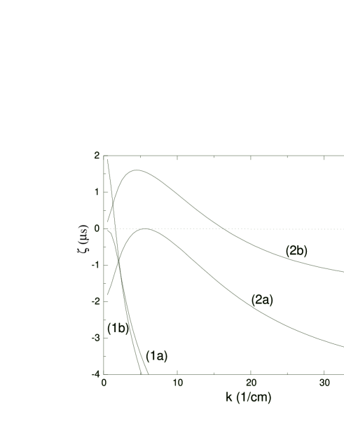
Figure 5 shows dispersion relations for the low current case. The calculations have been performed with two reduced values of the base conductivity in order to illustrate two qualitatively different instabilities that can occur in the semiconductor structure. If the base conductivity is sufficiently low, dispersion relations like the curves denoted by (2) can occur. They are characterized by a pronounced maximum at a critical wave-number that is definitely larger than zero. Curve (2a) represents the case that the increment of this critical wave-number is zero, while all other increments are still smaller than zero, i. e., the uniform state becomes destabilized with respect to current-density fluctuations with the critical wave-number. When the sample current is decreased, the curve is shifted up [curve (2b)], and the increments of a certain band of wave-numbers are larger than zero. This behavior can be interpreted as a Turing-like instability [1].
When the transversal coupling inside the thyristor-like subsystem is strengthened, e. g. by reducing the transversal resistance of the base, the maxima of shift to smaller values leading to dispersion relations like those denoted by (1). They are characterized by a monotonous decrease of with growing , which can be considered as an instability of Ridley’s type [18]. In such a case, the uniform state is typically destabilized via a saddle node bifurcation by fluctuations with the shortest possible wave-number , if uniform fluctuations are suppressed by a sufficiently large load resistor in the external circuit. Similar to the Turing-like case, the curve is shifted upwards, when the sample current is decreased. Note that the parameter is the same for the curves (1a) and (2b) and has been adjusted such that the differential resistance of the global current-density vs. voltage characteristic vanishes, i. e., .
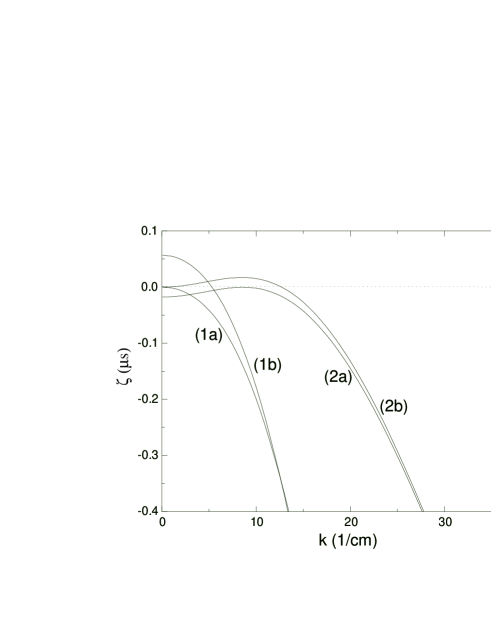
Dispersion relations for the moderate current case are shown in Fig. 6. Similar to the low current case the homogeneous state is destabilized at a critical current level either by an instability of Ridley’s (curves 1) or Turing’s type (curves 2). The bifurcation type can be controlled by a proper design. The most important parameters are the conductivities of the resistive layer, the and the base. The former essentially governs the transversal spreading of the potential drop across the resistive layer and tends to damp out current-density fluctuations. The and base conductivity control the transversal hole and electron current densities in the two base layers. As these base currents in turn regulate the injection of electrons and holes from the emitter and the plasma layer , respectively, they play an important role concerning the transversal spreading of a region with enhanced current density. The competition between the damping and the activating process, is the essential physical mechanism allowing - under properly chosen design parameters - the destabilization of a homogeneous current-density distribution by spatially periodic current-density fluctuations strongly reminding of the generic mechanism proposed by Turing.
VI Summary
In conclusion we point out that the suggested theory, which is based on a subdivision of the semiconductor structure into an active and a passive subsystem, supplies a self-consistent quantitative description of the nonlinear mechanisms, which control the longitudinal current flow, and the transversal current-density instabilities in multilayer semiconductor systems. The nonlinear longitudinal electrical properties in the active layer are based on a thyristor-like regenerative mechanism, while the passive subsystem acts as a simple resistive layer. Depending on the system parameters two different types of regenerative mechanisms can be distinguished leading to specific model equations. A stability analysis of the derived equations reveals that in each case two basic bifurcation types can be expected when the total sample current is varied. The bifurcations are caused by instability mechanisms that are closely related to those studied by Turing [1] and Ridley [18]. It turned out that in particular the conductivity ratios of the base, the plasma layer, and the resistive layer are important parameters to control the instability mechanism. Thus, adjusting the respective transversal conductivities, e. g., by irradiating the sample with protons or ions, using compensated substrate material, or adapting the sample geometry, it is possible to design a multilayer system with the aspired (in)stability features. Finally, we emphasize that the suggested approach presents a basis for further numerical analysis of pattern formation processes.
Acknowledgements
The present paper was prepared in the frame of the international project ”Dissipative Pattern Formations in Semiconductors and Semiconductor Devices” supported by the Deutsche Forschungsgemeinschaft and the Russian Academy of Science.
REFERENCES
- [1] A. Turing, Phil. Trans. Roy. Soc. B 237, 37 (1952).
- [2] G. Nicolis and I. Prigogine, Self-Organization in Non-Equilibrium Systems (Wiley, New-York, 1977).
- [3] H. Haken, Advanced Synergetics, 2nd ed. (Springer, Berlin, 1987).
- [4] B. Kerner and V.V. Osipov, Autosolitons (Kluwer, Dordrecht, 1994).
- [5] M. Mikhailov, Foundations of Synergetics, 2nd ed. (Springer, Heidelberg, 1994).
- [6] Self-Organization in Activator-Inhibitor Systems: Semiconductors, Gas-Discharges and Chemical Media, ed. by H. Engel et al. (W & T-Verlag, Berlin, 1996).
- [7] D. Walgraef, Spatio-Temporal Pattern Formation (Springer, New York 1997).
- [8] Evolution of Structures in Dissipative Continuous Systems, ed. by F.H. Busse and S.C. Müller (Springer, Berlin, Heidelberg 1998).
- [9] E. Schöll, Nonequilibrium Phase Transitions in Semiconductors (Springer, Berlin, 1987).
- [10] Nonlinear Dynamics and Pattern Formation in Semiconductors and Devices, ed. by F.-J. Niedernostheide (Springer, Berlin, 1995).
- [11] F.-J. Niedernostheide, M. Arps, R. Dohmen, H. Willebrand and H.-G. Purwins, Phys. Stat. Solidi B 172, 247 (1992).
- [12] A.V. Gorbatyuk, I.A. Linijchuk and A.V. Svirin, Sov. Tech. Phys. Lett. 15, 224 (1989) [Pis’ma Zh. Tekh. Fiz. 15, 42 (1989)].
- [13] A.V. Gorbatyuk and P.B. Rodin, J. Comm. Technol. Electron. 40, 49 (1995) [Radiotekhnika i êlektronika 40, 1876 (1994)].
- [14] A.V. Gorbatyuk and F.-J. Niedernostheide, Physica D 99, 339 (1996).
- [15] M. Bode and H.-G. Purwins, Physica D 86, 53 (1995).
- [16] D. Ruwisch, M. Bode, H.-J. Schulze and F.-J. Niedernostheide, in: Nonlinear Physics of Complex Systems, Lecture Notes in Physics, Vol. 476, ed. by J. Parisi, S. Müller, and W. Zimmermann (Springer, Berlin, Heidelberg, 1996), pp. 194-212.
- [17] I.V. Varlamov and V.V. Osipov, Sov. Phys. Semicond. 3, 803 (1969) [Fiz. Tekhn. Poluprovodn. 3, 950 (1969)].
- [18] B.K. Ridley, Phys. Soc. 82, 954 (1963).
- [19] A.V. Gorbatyuk and P.B. Rodin, Z. Phys. B 104, 45 (1997).
- [20] M. Meixner, P. Rodin, and E. Schöll, Phys. Rev. E 58, 2796 (1998), and Phys. Rev. E 58, 5586 (1998).
- [21] F.-J. Niedernostheide, B.S. Kerner und H.-G. Purwins, Phys. Rev. B 46, 7559 (1992).
- [22] F.-J. Niedernostheide, M. Ardes, M.Or-Guil und H.-G. Purwins, Phys. Rev. B 49, 7370 (1994).
- [23] F.-J. Niedernostheide, M. Or-Guil, M. Kleinkes und H.-G. Purwins, Phys. Rev. E 55, 4107 (1997).
- [24] A.V. Gorbatyuk, Dynamics and Stability of High Speed Retroaction Processes in Structures of Power Thyristors, A.F. Ioffe Institute Preprint 962, Leningrad (1985) (in Russian).
- [25] G.K. Wachutka, IEEE Trans. (ED) 38, 1516 (1991).
- [26] A.A. Jaecklin, IEEE Trans. (ED) 39, 1507 (1992).
- [27] A. Wierschem, F.-J. Niedernostheide, A.V. Gorbatyuk and H.-G. Purwins, Scanning 17, 106 (1995).
- [28] W. Gerlach, Thyristoren (Springer, Heidelberg, 1981) (in German).
- [29] S. M. Sze, Physics of Semiconductor Devices (Wiley, New-York, 1981).
- [30] N.H. Fletcher, Proc. IRE 45, 863 (1957).
| Symbol | Symbol meaning | Value |
|---|---|---|
| 2.8 | ||
| diffusion coefficient of electrons | ||
| diffusion coefficient of holes | ||
| Boltzmann constant | V/K | |
| intrinsic carrier concentration | cm-3 | |
| elementary charge | As | |
| vaccuum permittivity | F/cm | |
| dielectric constant of Si | 11.7 | |
| electron mobility | ||
| hole mobility | 480 cm2/Vs |
| Symbol | Symbol meaning | Value |
|---|---|---|
| saturation value of the electron injection current-density at the - junction | Acm-2 | |
| saturation value of the hole injection current-density at the - junction | Acm-2 | |
| saturation value of the recombination-generation current-density at the - junction | Acm-2 | |
| acceptor concentration of the emitter | cm-3 | |
| acceptor concentration of the bulk | cm-3 | |
| acceptor concentration of the base | cm-3 | |
| donor concentration of the base | cm-3 | |
| donor concentration of the emitter | cm-3 | |
| width of the base | cm | |
| width of the base for | cm | |
| width of the plasma layer | cm | |
| width of the resistive layer | 1 cm | |
| conductivity of the base | ||
| conductivity of the base | ||
| conductivity of the layer | ||
| conductivity of the bulk | ||
| lifetime in the layer for low currents | s | |
| lifetime in the layer for moderate currents | s |