,,,
Light ions response of silicon carbide detectors
Abstract
Silicon carbide (SiC) Schottky diodes 21 m thick with small surfaces and high N-dopant concentration have been used to detect alpha particles and low energy light ions. In particular 12C and 16O beams at incident energies between 5 and 18 MeV were used. The diode active-region depletion-thickness, the linearity of the response, energy resolution and signal rise-time were measured for different values of the applied reverse bias. Moreover the radiation damage on SiC diodes irradiated with 53 MeV 16O beam has been explored. The data show that SiC material is radiation harder than silicon but at least one order of magnitude less hard than epitaxial silicon diodes. An inversion in the signal was found at a fluence of 1015 ions/cm2.
keywords:
SiC-Silicon Carbide , Semiconductors , Radiation Detectors , Radiation DamagePACS:
29.40 , 07.85.F , 07.77.K ,1 Introduction
In the last years the use of electronic devices and sensors in very harsh environments at elevated temperatures, high-power, high-frequency and high radiation fields has became the subject of research and development in various fields. In particular the search for new materials, more suitable for such extreme operating conditions than the usual silicon semiconductor has received a lot of interest. Among the investigated materials, the silicon carbide (SiC) semiconductor has raised large interest and has been already used in a wide range of applications [1, 2, 3, 4, 5, 6, 7, 8]. In particular, recent work has been done on the development of SiC radiation detectors [9, 10] and on the characterization of their performances. SiC detectors were used with excellent results as neutron [11] and X-ray detectors operating at high temperatures [12]. The charged-particle response characteristics have been measured by irradiating the detectors with alpha particle sources at energies up to 5.48 MeV [13, 14, 15], and radiation damage effects were investigated with 24 GeV protons and gamma rays [16, 17, 18], 300 MeV/c pions [19], neutrons [20] and protons, alphas and 12C beams [21] at fluences up to 1016 particles/cm2 [20] obtaining promising results. Indeed one of the most appealing property of the SiC, as well as of other wide bandgap materials such as GaAs and diamond, is their predicted radiation hardness with respect to Silicon. Moreover SiC diodes show low reverse current even at the very high electrical voltage applicable because of their higher breakdown voltage with respect to Si. Both properties make SiC diodes suitable for the construction of specific detector arrays. The inner tracking detectors, typically used in the high-radiation environment of particle physics experiments, particle and ion detector arrays operating in satellites or in the very harsh environment of laboratories producing radioactive ion-beams would particularly benefit from the mentioned properties. In spite of the notable development in growing, processing and producing good-quality and low-defect SiC diodes, work to date on the use of such diodes as detectors of particles and ions has been very limited [13, 14, 15, 19, 21]. We have therefore studied the response signal of high-quality 4H-SiC Schottky diode to 12C and 16O ions and to an alpha particles source at various incident energies, in order to investigate the use of SiC detectors also in nuclear physics applications. The main objectives of the present work are the characterization of the signal response in term of linearity, energy resolution and rise-time as a function of the applied reverse bias and the investigation of its degradation subsequent to irradiation with light ions.
2 Experimental details
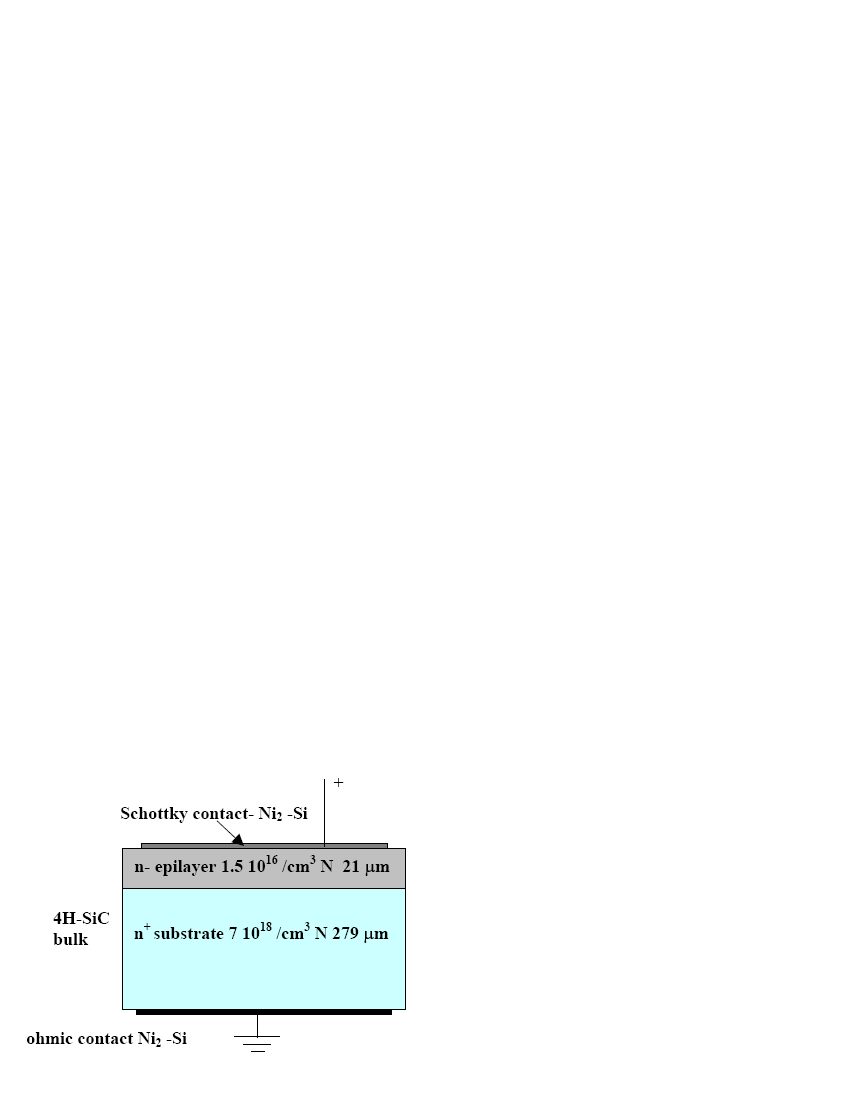
The Schottky diodes were fabricated by epitaxy onto high-purity
4H-SiC n-type substrate from the ETC-Catania [22].
Figure 1 shows the layout of the detector. The nominal
n- epitaxial layer nitrogen dopant concentration and thickness were,
respectively, 1.51016 N cm-3 and 21 m. The
dopant concentration and thickness of the n+ side were
respectively 71018 N cm-3 and 279 m. The net
doping and the thickness have been measured [22],
respectively, by C-V (Hg-probe) and FTR Biorad QS-500. The nominal
defects mean value was 43 cm-3 as measured [22] by
Raman spectroscopy with an Ar-laser at 514.5 nm.
The Schottky
junction was realized by a 0.2 m thick layer of Ni2Si
deposited at 600 ∘C on the front surface, while the ohmic
contact, on the back surface, was obtained with Ni2Si deposited
at 950∘C [23].
The active areas of the different SiC detectors were of 0.5x0.5, 1x1 and 2x2 mm2 (see Fig. 2). The chips were glued on a brass foil 1 mm thick by a conductive glue and single contacts between the Ni2Si front surfaces and the pads of the board shown in Figure 2 were realized by Al wire (2m thick) bonding.
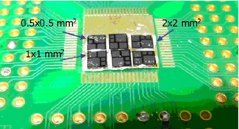
Two boards with respectively six and five chips 2x2 mm2 of surface were assembled, for a total number of eleven independent detectors. The third board was equipped with a Si detector 300 m thick and 3x3 cm2 of surface which was used as a reference. The three boards were set-up in a scattering chamber at the Laboratori Nazionali del Sud (LNS-Catania) and operated under vacuum at 10-6 mbar. The active samples were irradiated with both 5.48 MeV alpha particles from an 241Am source and 12C and 16O beams accelerated by the LNS Tandem VdG at different energies and currents. The alpha source was set-up at a distance of 10 cm from the detector surface in order to get a near normal incidence of alpha particles on the detector. The ion beams were focused 60 cm downstream with respect to the detector position in order to achieve an uniform perpendicular irradiation in a spot of about 3 mm of diameter on the SiC surface. The boards holder was moved so as to center the detectors one by one. Standard electronics was used to process the signals: preamplifiers of 45 mV/MeV gain and amplifiers with 0.5 sec shaping time. Data acquisition was based on CAMAC ADCs read out through a GPIB standard National Instruments interface and a data-acquisition program built in the LabView 7 framework. Moreover the preamplifier and amplifier signals were digitalized by a Tektronix TDS 5104B digital oscilloscope.
3 Detector response
It is well known that a reverse bias must be applied in order to
create in the diode a depleted region which acts as the active
region for the detection of the charges produced by
ionization from the incoming charged particles.
The order of magnitude of this reverse bias could be a relevant
parameter for specific applications. Therefore we measured at first
the correlation between the thickness of the depleted layer and the
applied bias, which is expected to follow a square-root law
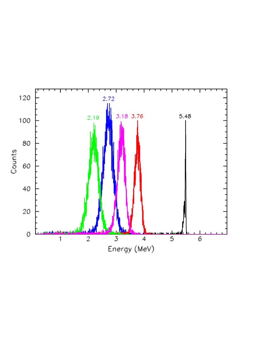
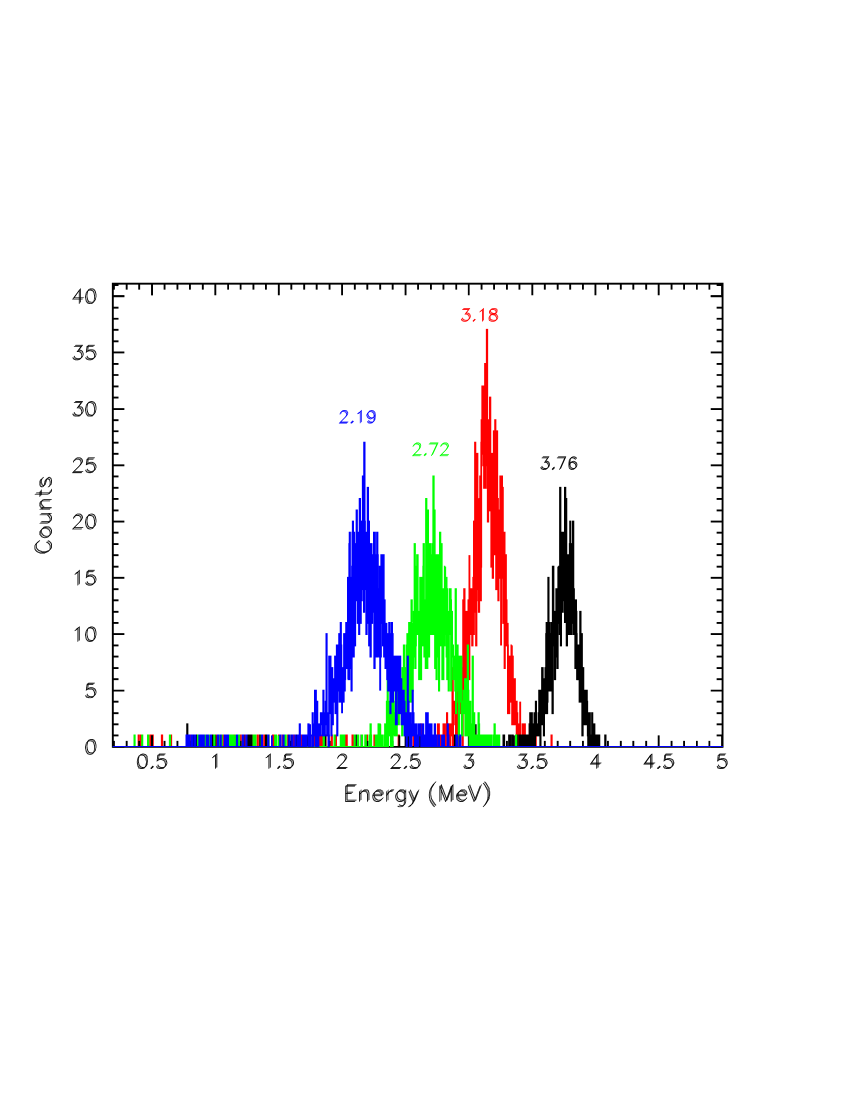
[24]. By using four Al absorbers of 10, 13, 14.6 and 17.3
m thicknesses, in front of the 241Am alpha source, we
scaled the incident energy from 5.48 MeV to 3.76, 3.18, 2.72 and
2.19 MeV respectively as measured by the calibrated silicon detector
(see Fig. 3).
Using the SRIM code [25] calculations, the ranges of the alpha particles at the four incident energies in the SiC material were evaluated to be: 10.80.4, 8.50.5, 7.00.6 and 5.40.5 m respectively. The errors on the range thickness were evaluated by taking into account both the energy loss in the Ni2Si 0.2 m thick front layer on the detector and the FWHM (full-width at half-maximum) of the alpha spectra of Fig. 3, in order to account for the energy straggling introduced by the Al absorbers. A typical set of spectra is shown in Fig. 4 for one of the detectors used. For all the detectors the centroid position of the peak moves toward higher channels as the voltage increases. The observed shift can be described according to the increasing thickness of the active volume of the detector with increasing reverse bias voltage.
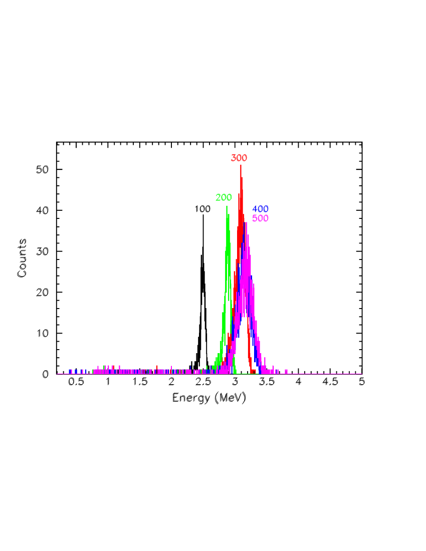
As a result, the incident alphas deposit more energy in the active
region leading to detector signals with higher pulse heights. The
saturation of the pulse height values is then reached when the
applied reverse voltage depletes the active volume of the diode up
to the range corresponding to the energy of the incoming alpha. For
a given alpha energy we then searched for the value of the applied
reverse bias at which the saturation of the pulse height signals is
reached (see Fig. 4-top panel). The correlation between
the evaluated range and the applied reverse voltage, shown in
Fig. 5, is nicely reproduced by a square-root law
[24].

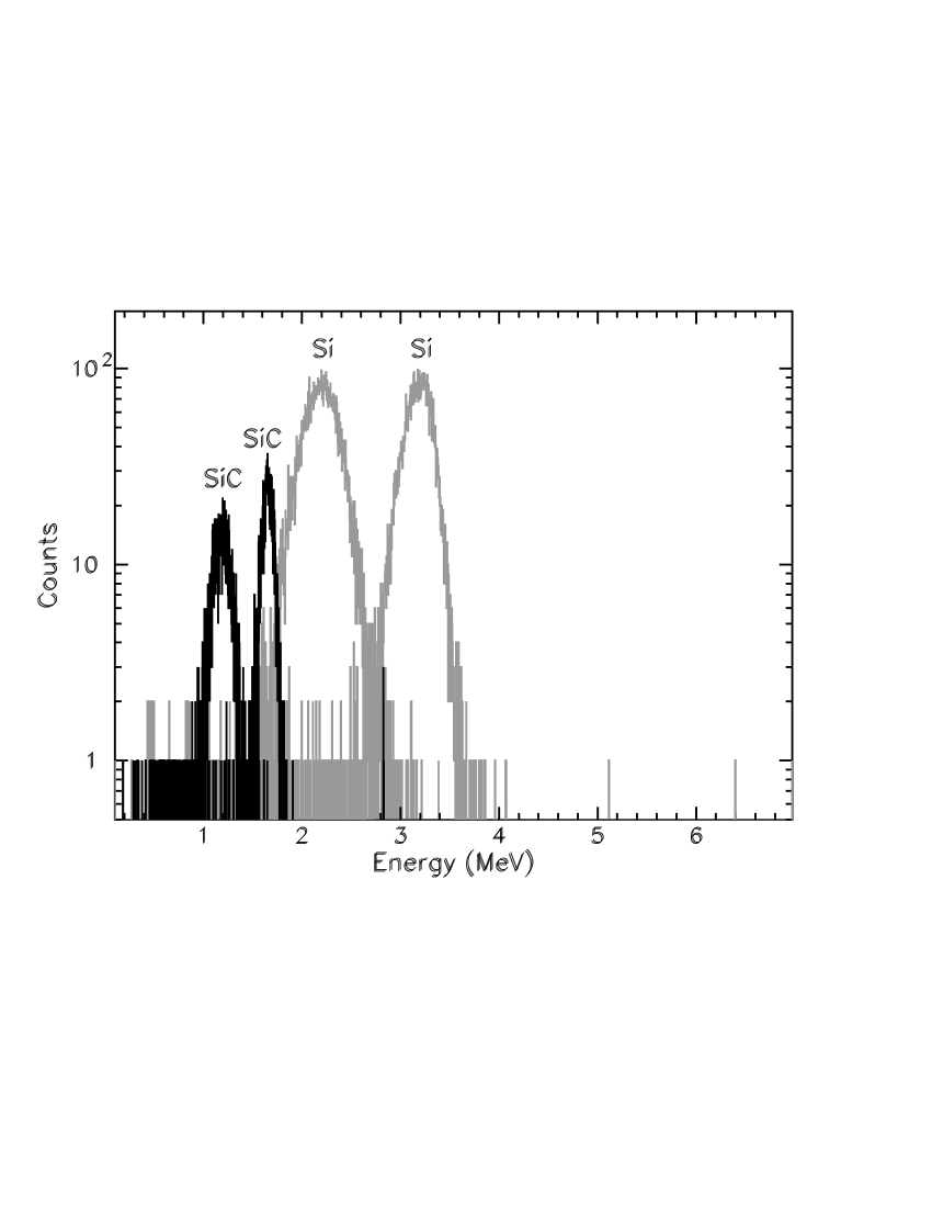
Finally, by correlating the saturated pulse height peak values and
the four alpha energies (2.08, 2.62, 3.09, 3.68 MeV) corrected for
the energy lost in the Ni2Si 0.2 m thick front layer of the
SiC diode, we calibrated the pulse height scale. By comparing the
energy peaks obtained with the SiC and the silicon detector for the
same deposited energy (see Fig. 6) we have obtained a
factor of 2.10.3 in the charge produced by ionization, as
expected from the different ionization energy values of 3.76 eV in
Si and of 7.74 eV, as recently measured [26, 27], in
SiC.
To increase the explored energy range we used beams of
12C at 5.06 and 17.68 MeV and 16O at 7.3, 9.78, 12.18 and
14.21 MeV of incident energies provided by the Tandem accelerator of
the LNS. The SiC diodes were operated at a reverse bias of -100V
which depletes the active region of the detector up to 5.40.5
m, wide enough to completely stop all the ions except the
12C at 17.68 MeV and the 16O at 14.21 MeV of incident
energy which, according to SRIM calculation, release around 8 and 13
MeV respectively in the detector. Fig. 7 shows the energy
spectra measured by the SiC diodes. The high degree of linearity
observed in the correlation between the pulse height and the energy
shown in Fig. 8 for SiC detectors, is consistent with
previous measurements [13, 14, 19], and indicates the
proportionality of the produced ionization charge to the deposited
energy.


Similarly to the measurements performed with the alpha source, a number of spectra were taken over a range of bias voltages, from 0 to - 450 V, for the 12C beam at 17.68 MeV incident energy ( see Fig. 7-bottom panel).

We notice in Fig. 7 that no saturation has been observed
in the peak centroid values, since the active region of the detector
does not extend beyond the range of the 12C at 17.68 MeV in
SiC, which is approximately 11.2 m. This occurrence indicates
that at the maximum applied bias voltage, - 450 V, the detector is
only about half depleted but, unfortunately, we could not raise the
bias voltage to higher values because the electrical connections in
vacuum were sparking at around -500 V.
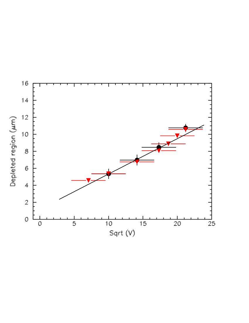
Therefore we evaluated the thickness of the depleted region by
comparing SRIM calculations to the energy loss measured at different
applied biases. Figure 9 shows the correlation between the
estimated thickness of the depletion layer and the applied reverse
bias for 12C ions. We remark the good agreement with the data
measured with alphas and the good linear correlation between the
depletion layer thickness and the square-root of the applied bias
values. From a linear fit (see Fig. 9), at zero bias
voltage we estimated an active region thickness of 1.18 m
resulting only from the Schottky contact potential, in good
agreement with the result of
Ref. [13].
In order to measure how the energy resolution behaves as a function of the thickness of the active region and therefore of the applied bias voltage, we analyzed the data reported in Fig. 7. A typical 12C 17.68 MeV response spectrum is shown in Fig. 10: the shape of the peak is well reproduced by a Gaussian function.
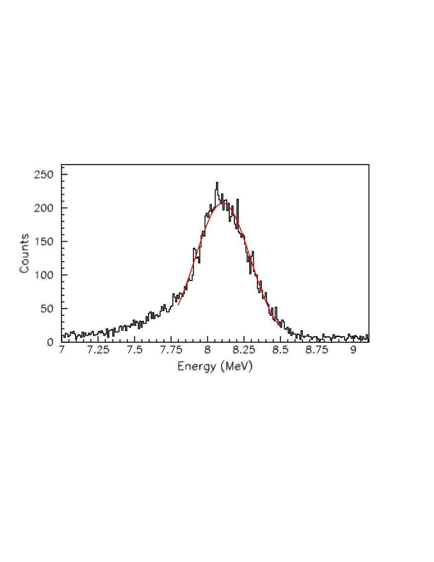

Based on the energy calibration, the full-width at half-maximum (FWHM) of the Gaussian fit to the 12C peak at 8.1 MeV (which is the energy lost in 5.4 m by the 12C at 17.68 MeV) is 190 keV corresponding to an energy resolution of 2.3%. In the bottom panel of Fig. 10, the relative energy resolution (FWHM of the peak over the peak position), is shown as a function of the applied bias voltage. Besides an initial enhancement from 0 to -50 V, the relative resolution decreases slowly over the range of the applied bias voltages up to a value of 1.8%. The measured energy resolution values are in good agreement with the ones observed in other measurements [14] although larger than the recently reported SiC energy resolution value of 0.34% [27, 28].
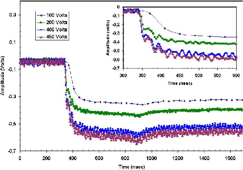
Moreover by storing the waveforms of the preamplifier output in the
Tektronix TDS 5104B Digital Oscilloscope we analyzed the behavior of
the pulses generated by the 12C beam at 17.68 MeV. Typical
pulses are reported in Fig. 11 for four different reverse
bias values. The amplitude variation is obviously related to the
increasing thickness of the active region and therefore to the
increasing energy lost by the 12C ions. The decrease of the
signal rise-time is related to the combined variations of the drift
velocity of the ionization charges, proportional to VBias, and
of the depleted region thickness, proportional to
.
Indeed, the rise-time varies from 97 nsec at
-100 Volts to 68 nsec at -200 Volts and reaches 46 and 44 nsec at
-400 and -450 Volts respectively. As expected the ratios of the
measured rise-time values scale as the inverse ratio of the
square-root of the applied bias voltages.
The consistency of the
SiC detectors performances were investigated by testing
charged-particle response of all the eleven detectors of identical
configuration. All of them showed, within the error bars, the same
characteristics here reported.
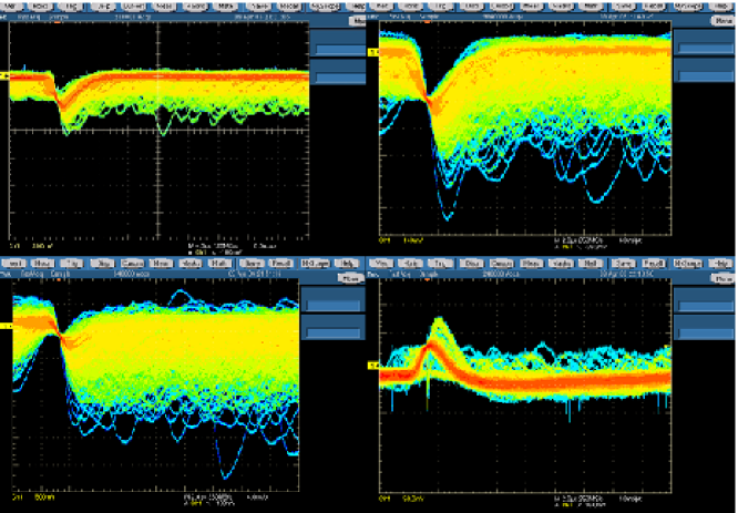
4 Radiation damage
One of the main motivations of such study was to explore the radiation hardness properties of such SiC detectors. Five samples were irradiated using 53 MeV 16O ions provided by the Tandem at the LNS-Catania and their output signals were monitored during the irradiation time. Fig. 12 shows the peak centroid of the 16O spectrum as a function of the fluence.

The applied reverse bias was kept fix at -100 V but the signals appeared to decrease in amplitude as the irradiation increased. The amplitude dropped to 50% at a fluence of 6.5 1014 ions/cm2 (see Fig. 12) in good agreement with results of Ref. [20, 29]. At the same time, the reverse current increased by a factor of five and the noise by a factor of two (see Fig. 13). The present SiC diodes are therefore around ten times radiation harder than silicon diodes but around a factor ten less hard than thin epitaxial Si-diodes for which the charge collection efficiency drops only to about 80% at 6 1015 protons/cm2 at 24 GeV of incident energy [30].
However it is not clear how to compare the damage produced by low
energetic 12C or 16O ions to the damage produced by
protons, neutrons, gammas or pions and which kind of defects, among
the known ones, are produced during irradiation.
Finally, two
different detectors were continuously observed during the
irradiation up to when they break-down at a fluence of 1015
ions/cm2. At this irradiation fluence we observed an inversion of
the signals with respect to the non-irradiated ones (see
Fig. 13: bottom-right panel). This effect seems similar to
the symmetric Charge Collection Efficiency (CCE) response at both
polarities mentioned in Ref.[20] at a
fluence of 1015 protons/cm2 and attributed to radiation damage.
Moreover, we inverted both bias and amplifier polarities and we sent
on the irradiated detectors an 16O beam at 12 MeV incident
energy. Since the applied reverse bias of -100 V depletes 5.4 m
of the SiC active region, we expected an energy release of 8.3 and
12 MeV in the detector from the 16O beam at 53 and 12 MeV
incident energy respectively, but the pulse height of the signal was
the same in both cases. Therefore we conclude that the detector was
sensitive to the charged ion but not to the deposited energy.
Further analysis will be performed to understand if the observed
effect is of the same nature of space-charge sign-inversion
(“type inversion”), reported for
Si-diodes [31, 32, 33]. At the moment we suggest, as
possible explanation, the formation of a layer of 16O
(1015 ions/cm2) at a distance of 27.20.4 m
(which is the range of the 53 MeV 16O ions in the SiC
material) from the Schottky contact, and therefore in the n+
type substrate, subdividing the 300m thick material in two
parts with a floating ground at the 16O layer.
5 Conclusions
In the present work we investigated the response of SiC Schottky
diodes to alphas, 12C and 16O low energetic ions in order
to explore the possibility of using these detectors in nuclear
physics applications in extreme environments. The signal response to
the ionization produced by the low-energy ions was analyzed in terms
of linearity, energy resolution, rise-time and deterioration as
function of the applied reverse bias and the irradiating fluence.
The latter measurements demonstrate the good quality of the SiC as a
radiation hard material.
Energy resolution on the order of 3% and
rise time up to 44 nsec have been measured at the maximum applied
reverse bias. The amplitude of the signal drops down to 50 % at a
fluence of 6.5 1014 ions/cm2 indicating more than an order
of magnitude hardness to the radiation with respect to silicon
diodes. The signal inversion at a fluence of 1015 ions/cm2
should be further investigated to understand if it is produced by
radiation damage or by the 16O implant in the material.
The
main inconvenience we have found in the use of the present detectors
was the high bias voltage, needed to deplete the active region of
the diode. We expect a correlation between the depleting bias values
and the N doping concentration in the epitaxial region [13].
We will investigate in the near future such a correlation, being
aware of the negative influence on the ionization charge production
and radiation hardness of a reduced doping concentration. But
reduction of the applied voltage to values far from the break down
ones is a very crucial issue for future applications.
6 Acknowledgements
The help in the SiC diodes selection and assembling and the valuable discussion with L.Calcagno, G.Foti and F.La Via are greatly appreciated. E.R. acknowledges the support from the European Community in the framework of the ”DIRAC secondary-beams” -contract N.515873 under the ”Structuring the European Research Area” Specific Programme Research Infrastructures action.
References
- [1] R.J. Trew, J.-B. Yan, P.M. Mock, Proc. IEEE 79 (1991) 598.
- [2] B.J. Baliga, Proc. IEEE 82 (1994) 1112.
- [3] C.E. Weitzel, C.E. Palmour, C.H. Carter Jr., K. Moore, K.J. Nordquist, S. Allen, C. Thero, M. Bhatnagar, IEEE Trans. Electron Dev. 43 (1996) 1732.
- [4] G.T. Heydt, B.J. Skromme, Applications of high power electronic switches in the electric power utility industry and the needs for high power switching devices, in: S.J. Pearton, R.J. Shul, E. Wolf gang, F. Ren, S. Tenconi (Eds.), Power Semiconductor Materials and Devices, Materials Research Society Symposia Proceedings, Vol.483, Materials Research Society, Warrandale, PA, 1998, p.3.
- [5] IEEE Trans. Electron Devices 46 (3) (1999) (number dedicated to silicon carbide).
- [6] J.A. Cooper, A. Agarwal, Proc. IEEE 90 (6) (2002) 956.
- [7] A. Elasser, T.P. Chow, Proc. IEEE 90 (6) (2002) 969.
- [8] R.C. Clarke, J.W. Palmour, Proc. IEEE 90 (6) (2002) 987.
- [9] M. Rogalla, K. Runge, A. Soldner-Rembold, Nucl. Phys. B 78 (Proc. Suppl.) (1999) 516.
- [10] M. Bruzzi, F. Nava, S. Russo, S. Sciortino, P. Vanni, Diam. Relat. Mater. 10 (2001) 657.
- [11] A.R. Dulloo, F.H. Ruddy, J.G. Seidel, J.M. Adams, J.S. Nico, D.M. Gilliam, Nucl. Instr. and Meth. A 422 (1999) 47.
- [12] G. Bertuccio, R. Casiraghi, A. Cetronio, C. Lanzieri, F. Nava, Nucl. Instr. and Meth. A 522 (2004) 413.
- [13] F. Nava, P. Vanni, C. Lanzieri, C. Canali, Nucl. Instr. and Meth. A 437 (1999) 354.
- [14] F.H. Ruddy, A.R. Dulloo, J.G. Seidel, J.W. Palmour, R. Singh, Nucl. Instr. Meth. A 505 (2003) 159
- [15] A. Kinoshita, M. Iwami, K. Kobayashi, I. Nakano, R. Tanaka, T. Kamiya, A. Ohi, T. Ohshima, Y. Fukushima, Nucl. Instr. Meth. A 541 (2005) 213
- [16] W. Cunningham, A. Gouldwell, G. Lamb, J. Scott, K. Mathieson, P. Roy, R. Bates, P. Thornton, K.M. Smith, R. Cusco, M. Glaser, M. Rahman, Nucl. Instr. and Meth. A 487 (2002) 33
- [17] F. Nava, E. Vittone, P. Vanni, G. Verzellesi, P.G. Fuochi, C. Lanzieri, M. Glaser, Nucl. Instr. and Meth. A 505 (2003) 645.
- [18] W. Cunningham, J. Melone, M. Horn, V. Kazukauskas, P. Roya, F. Doherty, M. Glaser, J. Vaitkus, M. Rahman, Nucl. Instr. and Meth. A 509 (2004) 127.
- [19] W. Cunningham, J. Melone, M. Horn, V. Kazukauskas, P. Roy, F. Doherty, M. Glaser, J. Vaitkus, M. Rahman, Nucl. Instr. and Meth. A 509 (2003) 127.
- [20] S. Sciortino, F. Hartjes, S. Lagomarsino, F. Nava, M. Brianzi, V. Cindro, C. Lanzieri, M. Moll, P. Vanni, Nucl. Instr. and Meth. A 552 (2005) 138
- [21] K.K. Lee, T. Ohshima, A. Saint, T. Kamiya, D.N. Jamieson, H. Itoh, Nucl. Instr. and Meth. B 210 (2003) 489.
- [22] E.T.C. Epitaxial Tecnology Center 207, Corso Italia I-95127 Catania -Italy
-
[23]
F. La Via, F. Roccaforte, A. Maktari, V. Raineri ,
P. Musumeci, L. Calcagno, Microelectronic
Engineering, Vol.60 (2002) 269
F. Roccaforte, F. La Via, V. Raineri, P. Musumeci and L. Calcagno, Appl. Phys. A (2003) 827 - [24] G.F. Knoll, Radiation Detection and Measurement, Third Edition, Wiley, New York, 2000, p.393
- [25] J.F. Ziegler, J.P. Biersack, IBM-research, Yorktown Heights, New York, USA, 1996.
- [26] G. Bertuccio and R. Casiraghi, IEEE Trans. Nuc. Sci. 50 (2003) 175
- [27] A. Ivanov, E. Kalinina, G. Kholuyanov, N. Stroka, G. Onushkin, A. Konstantinov, A. Hallen, A. Kuznetsov, in Silicon Carbide and Related Materials 2004, R. Nipoti, et al. (Eds.), Materials Science Forum 483-484, pp 1029-1032
- [28] F.H. Ruddy, J.G. Seidel, H.Chen, A.R. Dulloo,S. Ryu, IEEE Trans. Nucl. Sci. 53 [2006] 1713
- [29] T. Quinn, R. Bates, M. Bruzzi, W. Cunningham, K. Mathieson, M. Moll, T. Nelson, H.E. Nilsson, I. Pintillie, L. Reynolds, S. Sciortino, P. Sellin, H. Strachan, B.G. Svensson, J. Vaitkus, M. Rahman, IEEE Nuclear Science Symposium Portland, OR, USA, 19-25 Oct. 2003. Conference Record, Vol.2, p.1028-33, 2004. Ed. by S.D. Metzler, 2003
- [30] G. Lindström, E. Fretwurst, F. Honniger, G. Kramberger, M. Moller-Ivens, I. Pintilie, A. Schramm, Nucl. Instr. and Meth. A 556 (2006) 451
- [31] G. Lindström et al., ”ROSE Collaboration”, Nucl. Instr. and Meth. A 466 (2001) 308.
- [32] I.E. Anokhin, A.B. Rosenfeld, O.S. Zinets, Radiation Protection Dosimetry 101 (2002) 107-110.
- [33] L. Bosisio, S. Dittongo, E. Quai and I. Rachevskaia, IEEE Trans. Nucl. Sci., 50 (1) (2003) 219