Observation of Scattering and Absorption
Centers in Lead
Fluoride Crystals
Abstract
For the first time, lead fluoride is used as a fast and compact material in electromagnetic calorimetry. Excellent optical and mechanical properties of the pure Cherenkov crystals are necessary for the A4 collaboration to perform a measurement of the nucleon’s strange form factors. Visible scattering and absorption centers as well as surface damages have been investigated to characterize the quality of more than one thousand crystals. Besides, transmittance measurements have been performed on all crystals to reveal absorption bands produced by intrinsic or impurity related point-structure defects. As a consequence, 89 crystals had to be replaced by the Chinese manufacturer SICCAS.
Index Terms:
Absorption bands, crystal defects, cubic lead fluoride, electromagnetic calorimetry.I Introduction
Lead fluoride (PbF2) crystals have been studied as detectors in nuclear physics for some time [1]. Since 1993, large and transparent PbF2 crystals have been available for electromagnetic calorimetry. From that time on, several research groups in high energy physics have taken into consideration to use pure ionic or doped PbF2 as a prospective calorimeter material and beam tests with up to 25 crystals have been performed at different laboratories [2, 3]. In 1999, the A4 collaboration at the Mainz Microtron MAMI, Mainz, Germany began the construction of the first PbF2 calorimeter, which will eventually comprise 1022 crystals. In this parity violation experiment, polarized electrons are scattered off a liquid hydrogen target to examine the possible contribution of strangeness to the nucleon’s Dirac and Pauli form factors. The requirements on energy resolution, timing, compactness and radiation resistance raised by the measurement of ppm asymmetries are extremely high. For instance, an energy resolution in a crystal matrix has to be achieved to separate background events from elastic scattering processes. Furthermore, the detector signals have to be shorter than 20 ns otherwise the measured asymmetries might be falsified by pileup losses. Only PbF2 crystals of highest quality could fulfill those demands.
The remainder of this paper is organized as follows: Section II reviews some basic properties of the PbF2 compound and reports technical aspects of the crystals’ growing method. In Section III, scattering and absorption centers found in the crystals will be described. Absorption bands and spatial zones of absorption have been noticed in measurements of the longitudinal and transverse transmittance. A brief summary of those findings is given in Section IV. Observed flaws will be documented in Section V. The last section provides the conclusions and their implications to the A4 experiment.
II Properties of the Lead Fluoride Crystals
The compound has outstanding properties concerning its application as a Cherenkov detector, among them a high transmittance extending below 270 nm, a density of 7.77 g/cm3, a radiation length of only 0.93 cm and a Molière radius of 2.2 cm. The compound is usually found in a cubic lattice structure (-PbF2), but at high temperatures the orthorhombic -phase appears. Since the raw materials are comparatively cheap, the crystals could be produced at modest costs. The Shanghai Institute of Ceramics and Chinese Academy of Sciences, Shanghai, China (SICCAS) has grown more than 1100 -PbF2 mono-crystals under contract with the Institut für Kernphysik, Mainz, Germany. Those crystals have the geometry of pyramidal sectors with trapezoidal basis. Their average cross-section is mm2 at the front face and mm2 at the rear face and their lengths vary between 150.0 and 185.4 mm, corresponding to .
The Bridgman method used by SICCAS allowed them to grow several PbF2 ingots at the same time. To avoid multiple appearances of crystallization centers the prepared seeds are usually held at temperatures below the melting point of 1097 K whereas the surrounding melt is kept at higher temperatures. Using the Bridgman method the growing ingots are fixed in their positions and the movable crucible with the raw materials is pulled very slowly through a heating zone which is controlled by radio-frequency heaters. Like the alternative Czochralski method this technique has the disadvantage that the crystals could be spoiled by reception of impurities from the crucible. For this reason, SICCAS has investigated procedures to reduce the number of impurities in the PbF2 crystals to an acceptable level. One solution is the application of post-growth treatments where the crystals are annealed in a gaseous atmosphere, which can remove oxide and hydroxide ions from the crystals [4]. It is evident that the quality of the crystals had to be controlled carefully after their delivery to Mainz. Crystals had to be selected which met the stringent requirements. A dedicated program of measurements included the inspection of their longitudinal and transverse optical transmittance, the determination of optical non-uniformities, the study of the radiation resistance of small samples and the precise check of their mechanical dimensions against the specifications [5]. Briefly, the radiation resistance of the material was high, and induced damages could be cured by optical bleaching with blue or near ultraviolet light [6]. The crystals revealed an internal transmittance of 100%; defects like macroscopic cracks, texture, and inclusions, however, have been observed in most of the them.
III Observed Scattering Centers
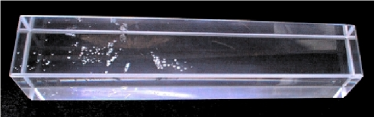
The optical setup for studying the PbF2 crystals consisted of a quartz tungsten halogen lamp, a condenser close to the light source, and an additional convex lens. The brightness was maximized and a highly uniform illumination of the crystal fixed in the first point of focus was provided. A screen was placed at the second point of focus to obtain a magnified and sharp image of a cross section through the crystal. In addition, photographs of illuminated crystals were taken. This led to the observation of several types of scattering centers and inclusions: needles, round shaped aggregates and irregularly formed inclusions. Some of the inclusions were colorless, some black, and only few white.
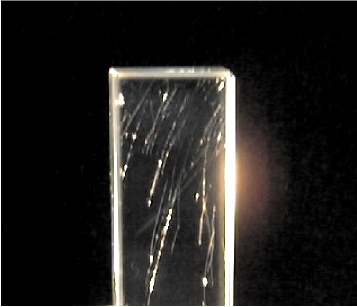
The needle-like inclusions started at the rear end of the crystals, which was the seed side in the growing process, and extended some centimeters. Their course was slightly bended, but followed the longitudinal axis of the crystal. Seemingly they originated from one-dimensional lattice defects during an early stage of the crystal’s production. During the crystals’ growth those defects have grown, too. As an example distinctly illuminated needle-like inclusions can be seen in Fig. 1(a). Similar observations in PbF2 crystals helped the manufacturer SICCAS to identify the needle-like inclusions with lead oxide or lead fluoro-oxide. [7], presents an analysis of Energy Dispersive Spectra measured at the Laboratory of Functional Inorganic Materials and states that the inclusions are mainly composed of lead, oxygen and fluor, and some of aluminum. A research group from SICCAS made dedicated experiments in order to reduce the forming of needle-like inclusions in PbF2 crystals, even if oxygen has been present in the melt. They succeeded by doping certain amounts of deoxidants into the system, by increasing the temperature gradient near the border between the growing mono-crystal and the melt as well as by reducing the speed of the crucible [7]. Nevertheless, about sixty of the crystals delivered to Mainz showed needle-like inclusions. Fortunately, neither did the inclusions cover the whole crystal volume, nor did they reduce the transmittance significantly.
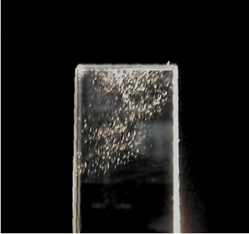
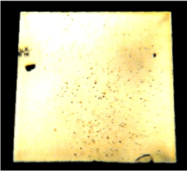
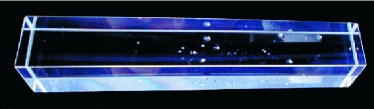
Another type of frequently observed scattering centers were round shaped aggregates. One example of the 33 crystals where this type of inclusion has been found is shown in Fig. 1(b). About 150 crystals revealed point-like scattering centers, which were too small to reduce the transmittance considerably. Fig. 2(a) presents a cross-section through a crystal with some black inclusions at the left corner and other inclusions at the bottom. In total, five crystals had black, irregularly shaped inclusions located directly below their surface. These defects supposedly originated in impurities that were present in the crucible during the growth process. In [7], some irregularly shaped inclusions are identified with orthorhombic PbF2 aggregates. This may result from an incomplete phase transition of -PbF2 into the -phase during the heating of the raw material.
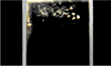
Apart from other defects, Fig. 3(a) shows larger aggregates grouped in several spatial domains of the crystal. Four crystals exhibited a texture of small microcracks that spread over a volume of some cubic centimeters. A further, but rare, observation was the appearance of white inclusions measuring about mm. This was noticed at the rear faces of some crystals after having coupled them to a photomultiplier, one is shown in Fig. 2(b). Presumably, the coupling procedure led to the transformation.
IV Observed Absorption Centers
In a real crystal, the symmetry of the lattice is always broken at some points. Those defects can lead to a reduction of the optical transmittance if they appear in high concentrations. Point-structure defects could be divided into impurity related defects, which are localized substitutional or interstitial, and intrinsic defects like trapped holes or interstitial Pb2+ or F- ions. The theoretical understanding of localized impurities in crystalline lattices is a difficult task and details could be determined only by calculating the embedding potential acting on the specific impurity. Intrinsic defects and electron density distributions could be modeled more accurately by quantum chemistry computer codes and it is known that the concentration of intrinsic defects, which are sometimes called thermal defects, increases exponentially with the temperature. A good measure of the defect concentration is the intensity of the related absorption bands in the transmittance spectra. The band characteristics depend very much on the quality of the raw material and the conditions during the growth process. Certain rare earth elements such as Cerium, Praseodymium, or Thulium are known to cause absorption bands at specific wavelengths. Key elements such as oxygen in the O2- form and hydrogen are particularly important.
The transmittancies of all PbF2 crystals have been determined between 200 and 800 nm by using a commercial double beam spectrophotometer Shimadzu UV-2101 PC. A very large sized compartment with a maximum probe length of 300 mm was used to measure the transmittance, not only transverse, but also longitudinal to the crystals’ axes. An integrating sphere collected all light passing through the samples to avoid corrections normally required by the nonparallel sides of the crystals. Assuming that the crystals have two parallel end faces, the reflections of the light beam limit the maximum transmittance to about 82% at 500 nm. The average values of the longitudinal transmittancies of all inspected crystals, including the rejected ones, were determined to be 80.4% at 800 nm, 74.1% at 400 nm, 64.8% at 330 nm, and 15.1% at 270 nm. These results were far better than the required specification limits of 75%, 70%, 58%, and 2% at the specified wavelengths demonstrating the high optical quality of a majority of the PbF2 mono-crystals. Nevertheless, about 50 crystals exhibited prominent absorption bands. Mostly they were located at wavelengths of 295 nm, 395 nm and 460 nm corresponding to transition energies of 4.2 eV, 3.1 eV and 2.7 eV, respectively. In some cases broad but weak absorption bands were present at 560 nm (2.2 eV) and 595 nm (2.1 eV). Fig. 4 shows some selected transmittancies where absorption bands are visible. Unfortunately, it was not possible to correlate specific impurities or defects with the observed absorption bands.
The crystals were scanned transverse to the longitudinal axis in steps of 5 mm between the front and the rear side in order to investigate spatial zones of absorption as well. A large fraction of the crystals did not show any, but in a considerable number of the investigated crystals spatial zones of absorption were found at different distances to the crystals’ seed sides. In Fig. 5 the transverse transmittance at 1, 4, 8 and 12 cm distance is shown for four selected crystals. As an example of a high spatial dependence of absorption centers crystal S1 021 is shown in Fig. 5(d). Fig. 5(b) exhibits the transmittance of crystal S3 058 with a small, but constant spatial gradient of absorption centers from one side to the other. In contrast, the measurements of crystal S6 063 reveal in Fig. 5(a) a strongly varying spatial gradient of the transmittance. In crystal S7 110, an absorption zone was found in the front part, but a high and uniform transmittance at larger distances as indicated by the three curves in Fig. 5(c) which are laying on top of each other. Such an absorption zone that is located at that part of the crystal, which was grown in a later stage of the production process, was typical for the majority of the affected crystals. The measured transmittancies of the crystals in Fig. 4 showed this type of spatial dependence as well.


V Observed Crystal Flaws
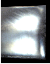
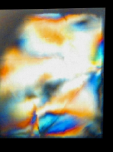
Even flaws which cannot be explained by impurities or lattice defects might affect the quality of the crystals. Stress regions inside the bulk material which indicate domains of possible micro or macro cracks could be made perceptible by looking for birefringence in the crystals. Birefringence of light beams appears when the isotropic lattice of a crystal is deformed by external or internal forces. Putting two perpendicular polarizers in front of and behind the crystal in the described optical setup exhibited colorful domains at a small number of crystals, where the shape and appearance of the domains were linked to the internal stress.
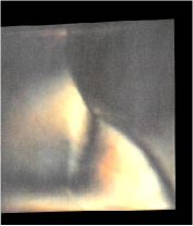
In Fig. 6(a), stress regions in the corners of a crystal can be recognized. They were characteristic for the greatest part of the investigated crystals and are supposedly due to the mechanical treatments like cutting or polishing. Fig. 6(b) presents a large crack diagonal to the longitudinal axis of the crystal which has probably been caused by internal stress. Fig. 6(c) shows an externally stressed crystal which was exposed to an electron beam of 20 nA intensity, causing strong temperature gradients by the high amount of deposited energy in a short time.
Smaller flaws or cracks in the material could be found in almost 300 crystals. Again, thermal stress due to high temperature gradients, which can occur during the annealing process, can be considered as the main reason for cracks in the crystals. Bigger splintering, as it is seen in the crystal of Fig. 3(b), could hardly be found, whereas smaller damages of the crystals’ faces were stated very often. Visible scratches, for instance, were observed at more than 200 crystals. Milky
streaks on the surface have been noticed at about 270 crystals, where the transmittance transverse to the crystal axis degraded by more than 15%. A typical crystal with milky streaks revealed transmittance values of 60% at 800 nm, 50% at 400 nm and 40% at 330 nm. The streaks appeared on the surface of the crystals and were caused by humidity, since PbF2 is slightly hygroscopic. They could not dissolved with acetone or any other appropriate method. The crystals most affected exhibited transmittancies below 30% in the entire spectrum.


VI Conclusions
The optical properties of 1100 PbF2 crystals grown by SICCAS for the A4 experiment have been studied. Minor defects like small scattering centers or surface damages have been found in 87% of the crystals. In general, the optical transmittance of all the crystals was high and close to the theoretical limit with a sharp band edge and without absorption bands. A high concentration of intrinsic or impurity related defects or scattering centers were found to be responsible for
a low optical quality of a small number of crystals. In some cases scattering centers even covered large parts of the crystals. Additional measurements of the transmittance exhibited absorption bands at specific wavelengths. Only about 140 crystals were transparent without any defects. Since the Chinese manufacturer SICCAS had guaranteed a certain optical quality, the replaced 89 crystals which had revealed low transmittance curves, strong absorption bands, or surface damages. The presented observations will allow the producer to understand the impurity and defect structure of PbF2 mono-crystals, and to improve their growing methods.
The measurements of the transmittance and the characterization of all crystals allowed the A4 collaboration to select appropriate crystals which met the stringent demands of its experiment. Combined with the inspections of the mechanical dimensions using a computer-controlled distance-measuring [5] and the results of the radiation resistance measurements [6], 171 crystals were returned to SICCAS for reuse as raw crystal growing material. After having finished this quality control program, the setup of one-half of the calorimeter solid angle has been completed. In July 2000, a successful data-taking
period with 511 PbF2 detectors confirmed the excellent optical properties of the selected crystals. Most of them fulfilled the stringent requirement on energy resolution. The experiment is in progress, and the collaboration will present results in a forthcoming publication.
References
- [1] D. F. Anderson, M. Kobayashi, C. L. Woody, and Y. Yoshimura, “Lead fluoride: an ultra-compact Cherenkov radiator for em calorimetry,” Nucl. Instrum. Meth. Phys. Res., vol. A290, pp. 385–389, May 1990.
- [2] C. L. Woody, J. A. Kierstead, P. W. Levy, S. Stoll, A. B. Weingarten, D. F. Anderson, E. J. Ramberg, Y. Kuno, J. A. Macdonald, A. Konaka, and D. A. Hutcheon, “A study on the use of lead fluoride for electromagnetic calorimetry,” IEEE Trans. Nucl. Sci., vol. 40, pp. 546–551, Aug. 1993.
- [3] R. D. Appuhn, F. Brasse, T. Deckers, H. Kolanoski, V. Korbel, A. Lindner, K. Meier, S. Spielmann, S. Valkar, A. Walther, and D. Wegener, “Electromagnetic calorimetry with lead fluoride crystals,” Nucl. Instrum. Meth. Phys. Res., vol. A350, pp. 208–215, Oct./Nov. 1994.
- [4] Shen Dingzhong, Yuan Xianglong, Zhang Lixin, Deng Qun, Li Peijun, and Yin Zhiwen, “Large size crystal growth for beta-lead fluoride” (in Chinese), J. Chinese Ceramic Soc., vol. 23, no. 6, pp. 667–672, Dec. 1995.
- [5] “Jahresbericht 1998–1999” (in German), biannual report, Institut für Kernphysik, Johannes Gutenberg-Universität, Mainz, May 2000.
- [6] P. Achenbach, I. Altarev, K. Grimm, T. Hammel, D. von Harrach, J. Hoffmann, H. Hofmann, E.-M. Kabuß, S. Köbis, A. Lopes Ginja, F.E. Maas, and H. Ströher, “Radiation resistance and optical properties of lead fluoride Cherenkov crystals,” Nucl. Instrum. Meth. Phys. Res., vol. A416, no. 2–3, pp. 357–363, 1998.
- [7] Ren Guohao, Shen Dingzhong, Wang Shaohua, and Yin Zhiwen, “Observation on scattering centers in PbF2 crystal,” in Proc. Int. Conf. Inorganic Scintillators Applications (SCINT97), Yin Zhiwen, Feng Xiqi, Li Peijun, and Xue Zhilin, Eds. Shanghai, China: Shanghai Branch Press, Sept. 1997, pp. 395–398.