A Current Mode Detector Array for Gamma-Ray Asymmetry Measurements
Abstract
We have built a CsI(Tl) -ray detector array for the NPDGamma experiment to search for a small parity-violating directional asymmetry in the angular distribution of MeV -rays from the capture of polarized cold neutrons by protons with a sensitivity of several ppb. The weak pion-nucleon coupling constant can be determined from this asymmetry. The small size of the asymmetry requires a high cold neutron flux, control of systematic errors at the ppb level, and the use of current mode -ray detection with vacuum photo diodes and low-noise solid-state preamplifiers. The average detector photoelectron yield was determined to be 1300 photoelectrons per MeV. The RMS width seen in the measurement is therefore dominated by the fluctuations in the number of rays absorbed in the detector (counting statistics) rather than the intrinsic detector noise. The detectors were tested for noise performance, sensitivity to magnetic fields, pedestal stability and cosmic background. False asymmetries due to gain changes and electronic pickup in the detector system were measured to be consistent with zero to an accuracy of in a few hours. We report on the design, operating criteria, and the results of measurements performed to test the detector array.
keywords:
parity violation , CsI detector array , radiative neutron capture , current mode , shot noise , gamma detectorPACS:
11.30.Er , 13.75.Cs , 07.85.-m , 25.40.Lw, , , , , , , , , , , , , , , , ,
1 Introduction
Bright pulsed spallation neutron sources possess high instantaneous neutron fluxes and also lend themselves to the measurement of neutron energy by time of flight. New high precision fundamental neutron physics experiments can be designed to take advantage of these features [1]. One such class of measurements consists of searches for parity violation in polarized neutron capture on light nuclei [2, 3, 4].
NPDGamma, currently under commissioning at the Los Alamos Neutron Science Center (LANSCE), is one such experiment. It is the first experiment designed for the new pulsed cold neutron beam line, flight path 12, at LANSCE. NPDGamma will determine the small weak pion-nucleon coupling constant, , in the N-N interaction [5, 6, 7]. This coupling constant is directly proportional to the parity-violating up-down asymmetry, , in the angular distribution of 2.2 MeV -rays with respect to the neutron spin direction in the reaction ,
| (1) |
The asymmetry has a predicted size of [8] and the goal of the NPDGamma collaboration is to measure it to 10% of this value. The small size of the asymmetry imposes stringent requirements on the performance of the beam line and apparatus. It is necessary to achieve high counting statistics while at the same time suppressing any systematic errors below the statistical limit.
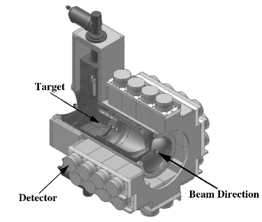
The experiment makes use of an intense cold neutron beam at LANSCE [12]. The beam is pulsed at 20 Hz and transversely polarized by transmission through a polarized 3He cell. A radio frequency spin flipper is used to reverse the neutron spin direction on a pulse-by-pulse basis. The neutrons are captured in a l liquid para-hydrogen target. The 2.2 MeV -rays from the capture reaction are detected by an array of 48 CsI(Tl) detectors. The entire apparatus is located in a homogeneous G magnetic field to maintain the neutron spin downstream of the polarizer and to suppress Stern-Gerlach steering of the neutrons. Three 3He ion chambers are used to monitor beam intensity, measure beam polarization and transmission and monitor the ortho-para ratio in the liquid hydrogen target.
To measure to an accuracy of , the experiment must detect at least a few -rays from capture with high efficiency. The average rate of -rays deposited in the detectors for any reasonable run-time is therefore high, and the instantaneous rates at a pulsed neutron source are, of course, even higher than for a CW source. Because of these high rates and for a number of other reasons discussed below, the detector array uses accurate current mode detection. Current mode detection is performed by converting the scintillation light from CsI(Tl) detectors to current signals using vacuum photo diodes (VPD), and the photocurrents are converted to voltages and amplified by low-noise solid-state electronics.
Another stringent constraint for the detector system is the detection and elimination of any instrumental systematic effects inducing false asymmetries associated with imperfections in the detector or data acquisition (DAQ) system. These effects must be measured periodically in the course of the experiment. It is therefore essential to perform these measurements in a short time, compared to the run time of the experiment. The time required for these measurements is determined by the time required to average the electronic noise. For the current mode detection to be effective the electrical noise in the detector system must be much smaller than the beam-on shot noise.
A series of measurements have been performed both on individual detectors and their components as well as on the detector array as a whole, in conjunction with the DAQ. The results show that the detectors meet all requirements described above. The remainder of this paper describes the measurements in detail, including the setup, the procedures used and the results found. In particular, we report on:
Several other characteristics of the detector array, such as long term gain fluctuations and counting statistics performance, have to be studied with a strong -ray source and are thus best done with capture -rays in a cold neutron beam. These tests have also been conducted and will be discussed in a forthcoming paper.
2 Detector Design and Operational Criteria
The detector array consists of 48 CsI(Tl) cubes arranged in a cylindrical pattern in 4 rings of 12 detectors each around a cylindrical l liquid hydrogen target (Fig. 1). In addition to the conditions set on the detector array by the need to preserve statistical accuracy and suppress systematic effects (see Section 2.4), the array was also designed to satisfy criteria of sufficient spatial and angular resolution, high efficiency, and large solid angle coverage. Here we discuss some of the reasoning behind certain design choices and describe the specific properties of our array.
To measure the asymmetry, a small () parity-violating component must be detected in the presence of an intense isotropic (parity-conserving) signal. The parity-odd component of the signal is proportional to , where is the angle between the direction of neutron polarization and the momentum vector of the emitted -ray. As long as the change in over a detector element is small, the finite size of the detector elements will not reduce the statistical accuracy of the experiment. From a calculation of the average over the solid angle of a detector, the error in the measured asymmetry due to spatial resolution, for detected -rays, is for an infinitely fine grained array and for an array with only two detectors, one covering each hemisphere [5]. Since the error is a slowly-varying function of the degree of segmentation, there is no pressing need for the detectors to be finely segmented, and the lateral dimensions can be chosen with regard to other criteria.
A segmented detector with elements large enough to fully contain the energy reduces the noise per detector from fluctuations in the fraction of energy shared among different detectors and simplifies the identification of the emission angle, which as noted above need not be determined with high precision. cross sections in high Z materials reach a minimum around MeV energy and the corresponding mean free path ( cm for MeV -rays in CsI) sets the scale for the dimensions of the detector elements. The size of the individual detectors is . With these dimensions each crystal absorbs about 84% of the energy for a MeV -ray incident at the center of the front face. MCNP111MCNP is a trademark of the Regents of the University of California, Los Alamos National Laboratory, http://laws.lanl.gov/x5/MCNP/index.html. [9] and EGS4222The EGS code system and its various tools and utilities are copyrighted jointly by Stanford University and National Research Council of Canada. All rights reserved. http://www.slac.stanford.edu/egs/. [10] calculations have shown that about 3% of the energy is backscattered from the front face of the crystal, 11% leaks out through the rear face, and 2% leaves through the 4 remaining sides. This reduces the cross talk between detector elements to a level that is small enough to allow the measurement of the asymmetry to the proposed accuracy. The main effect of cross talk is a small loss in angular resolution. A 20% increase in thickness in the direction of the incident -ray increases the amount of energy absorption by only 4%.
The overall size of the array, on the other hand, is constrained by the size of the source (target), which depends on the diameter of the neutron beam and the mean free path of a cold neutron in the liquid hydrogen target ( cm for a 2 meV neutron). The liquid hydrogen target is large enough to stop most of the neutron beam. Monte Carlo calculations performed using the double differential scattering cross sections for cold neutron scattering in liquid parahydrogen [11] indicate that a cm diameter, cm long target will capture about % of the incident neutrons [5]. These calculations are based on the neutron energy spectrum emitted by the coupled moderator viewed by the NPDGamma beam line [12]. The neutrons that are not captured in the liquid hydrogen are absorbed in a thin ( mm) plastic material loaded with 6Li to prevent activation of the CsI by neutron capture. -Rays are transmitted through the low Z of the plastic and the aluminum target vessel with high efficiency. Since neutron absorption in 6Li is dominated by charged particle emission as opposed to emission, background -rays which can dilute the signal from n-p capture are suppressed. For design purposes we can therefore choose to concentrate on the signal from n-p capture events rather than background events.
The detector array is arranged in cylindrical rings to surround most of the hydrogen target and allow the neutron beam to enter and exit without activating the CsI. It is important to detect the majority of the photons emitted transverse to the neutron beam, since the neutrons are transversely polarized and -rays emitted along the neutron polarization direction contribute most to the parity-odd component of the asymmetry. Photons emitted along the beam direction therefore contribute little to the asymmetry, and the question becomes how many rings need to be included. Monte Carlo calculations have shown that the error in the asymmetry as a function of the number of rings along the neutron beam axis reaches % of its asymptotic value for 4 rings [5]. Together with the individual detector dimensions mentioned above this geometry covers a solid angle of nearly 3.
With the detector size chosen to be large compared to the mean free path, the predicted peak rate into a single detector in the experiment is estimated to be MHz, based on moderator brightness measurements [12] and Monte Carlo calculations. At this rate pulse counting is impractical for CsI given the decay time of the scintillation light pulses (1 [13, 14]). For an array composed of CsI detectors, the high photon rates must be handled using current mode detection.
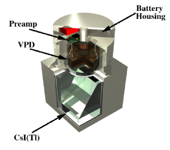
The crystals were manufactured and encased in the housing by Bicron 333Bicron, Saint-Gobian Industrial Ceramics, Inc. www.bicron.com. Each detector module consists of two rectangular pieces of optically coupled Thallium doped Cesium Iodide crystals. The slightly hygroscopic CsI(Tl) crystals are wrapped in PTFE Teflon, a diffuse reflector, and hermetically sealed in a thick Aluminum housing. The Optics program [15] was used to study which reflector and crystal surface treatment to use, in order to obtain the maximum light output and best overall uniformity for the given detector geometry. We found that diffuse reflection produced the best results. The crystals are coupled to a diameter K+ glass window at the top of the housing assembly to facilitate the detection of the scintillation light by a vacuum photodiode (VPD) during standard operation. The detectors are individually mounted on the array to minimize potential stress and plastic deformation of the crystals.
CsI(Tl) was chosen because of its high density (), large Z, high light yield and its relatively low cost. For the alkali iodides, thallium activation is required to achieve a high light output. For CsI(Tl) the emitted scintillation light has a wavelength centered around which is well matched with the absorption characteristics of the type of VPD used in this experiment. The light yield of CsI(Tl) is 54000 photons per MeV at maximum emission and with a scintillation efficiency of 12% [16]. The current collected from the VPD anode is amplified by a low noise solid-state amplifier.
A cylindrical aluminum housing for the VPD and preamplifier is mounted on top of the CsI crystal assembly. The housing is designed to be light-tight, to minimize noise contributions from capacitive coupling between electronic components on the preamplifier board and to shield the assembly from outside fields such as those produced by the radio frequency spin flipper. To avoid ground loops the detector housing is grounded via the signal cable shield only and the detectors are individually mounted to a stand which allows the electrical isolation between detectors. Each detector comes equipped with two light emitting diodes (LED), one in each crystal half. The LEDs are used during beam off detector diagnostic tests (see Section 4.3).
Radiation damage will decrease the self-transparency of the crystals, resulting in a decrease in detected light. CsI(Tl) has been found to be rather radiation hard up to doses of more than Gy [17, 18, 19, 20, 21], with the precise threshold for significant radiation damage in the crystal dependent on crystal impurities as well as the radiation damage rate. This radiation dose is approximately the dose that the detectors will receive over the course of the entire experiment (a few thousand hours of running), and the corresponding damage rate is small compared to those that have caused significant radiation damage in CsI(Tl) detectors in the past.
2.1 Vacuum Photodiodes
To convert the scintillation light to a current the detectors employ mm S-20 Hamamatsu 444 VPD type R2046PT, Hamamatsu Corporation, 360 Foothill Road, P.O. Box 6910, Bridgewater, N.J. 08807-0910, USA, www.hamamatsu.com vacuum photodiodes rather than photomultiplier tubes (PMT). The decision to use VPDs was based on the fact that photomultipliers are very sensitive to magnetic fields. A G field leaking into the PMT can change its gain by 100%. The experiment uses magnetic fields to control the neutron spin direction and any field leaking into the detectors may produce large gain changes. On the other hand, the sensitivity of a vacuum photodiode to magnetic fields is only about in a G DC field or for G AC field (see Section 3.2) [22].
This particular type of vacuum-photodiode was chosen for the low photocathode sheet resistivity. The low sheet resistivity of the S-20 photocathode reduces the degree of gain non-linearities across its surface.With an S-20 cathode, the VPD has a quantum efficiency of at the CsI maximum emission wavelength. A bias of Volts is applied across the VPD via two V batteries located on top of the VPD and preamplifier housing (Fig. 2). This removes the necessity for an external supply to be connected directly to the VPDs which could cause ground loops and introduce additional noise in the VPDs. The batteries 555Eveready Industries India, LTD. , www.evereadyindustries.com have a capacity of mAh, the average beam-on current drawn from the VPDs is about nA and the VPDs can therefore nominally be run for hours continuously. So the time before exchange should be limited by the battery’s five year shelf life.
Photodiodes are known to be extremely linear devices. Bench tests with the photodiodes used in the experiment have shown that their gain is uniform to better than per nA of photocathode current up to 500 nA. The typical peak photocathode current per detector for the NPDGamma experiment is nA, while pulse-to-pulse fluctuations seen by the detectors are typically less than 1%.
2.2 Low Noise Preamplifier
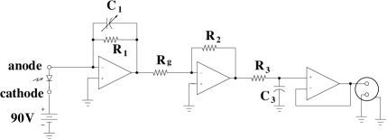
The VPD current in each detector is converted to a voltage signal by a three stage low-noise current-to-voltage preamplifier [23]. The first stage uses an op amp-based current-to-voltage amplifier with a gain of (Fig. 3). The second amplifier stage serves as an inverter with a nominal gain of . The resistors in the second stage are used to adjust relative detector gains (see Section 2.3 and 3.4). The third stage serves as a low impedance line driver.
The detector preamplifier has been designed to operate at noise levels close to the theoretical limits set by Johnson noise, so that the time required to measure the asymmetry to the level of is dominated by the collection of counting statistics rather than by the need to average electronic noise [24]. Various filter stages and ground isolation between the preamp power and signal circuit have been implemented to satisfy these requirements.
2.3 Data Acquisition and Storage
Because of the small size of the parity violating signal and the presence of the large isotropic signal, the intensities within each of the 8 near detectors and each of the 4 corner detectors in a given ring are nearly equal. It is therefore possible to equalize the signals from near and corner detectors by gain adjustments (discussed below) and sample only (1) the average signal in a ring, (2) the differences in each detector from the average signal in a ring. This strategy allows one to exploit the increased dynamic range to increase the gain of the system and minimize the effects of noise in the sampling electronics. Here we describe the details of how this idea for sampling the array signals was implemented.
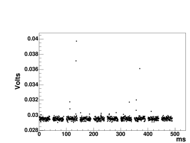
The preamplifier output for each detector is sampled by the NPDGamma data acquisition. The DAQ incorporates four sum and difference amplifier boards with 12 channels each. Each sum and difference board forms an average voltage over the 12 detectors in a given ring and each individual detector signal has its corresponding ring average subtracted. The process is shown schematically in Fig. 4. Here each difference amplifier contributes a gain factor of 10 and each Bessel filter (denoted by F in the schematic) contributes an additional factor of 3 to the gain. The 48 resulting difference signals and four average signals are sampled by 16-bit ADCs. The sum and difference signals are sampled at kHz and kHz respectively. A macro pulse of data is collected by sampling for a duration of ms, followed by a ms break, before the next frame of neutrons arrives. This results in 2000 difference and 2500 sum samples for each macro pulse. In the data stream (before the raw data are written to file) every group of 20 difference samples and 25 sum samples is summed to produce a final value for each of 100, ms wide time bins. The sampled data are transfered via fiber optic connection to a 3.5 Tbyte RAID array storage device. Figure 5 shows the 10 macro pulses of electronic pedestal (beam off) output for a typical detector, obtained using the described sampling scheme.

According to Fig. 4 and the sampling scheme just described, the data actually stored for each time bin are a sum of 20 difference samples for each detector and a sum of 25 average samples for each ring . A ring average sample is given by and a difference sample for a given detector in the ring is given by . In the analysis, the time bin average of the difference and sum signals are recombined to produce the average detector signal for the time bin at the ADC input , in ADC counts. Here, and .
The sum and difference scheme increases the effective dynamic range of the ADCs, which are limited to V, therefore allowing for a larger gain to be applied and staying above the bit-noise of the ADCs. The Bessel filters provide highly correlated ADC samples, filtering out high frequency components in the signal, and the high sampling rate averages out the bit noise in the ADCs. The chosen time bin width removes the correlation between the data points actually used in the calculation of asymmetries (see Section 4.1).
2.4 Mode of Operation and Systematic Effects
Achieving the desired accuracy in measuring the parity violating asymmetry depends on good counting statistics with comparatively small errors from other sources, such as electronic noise and systematic effects. During beam-off measurements, the time required to determine any systematic effect is governed by the noise in the preamplifier and the rest of the DAQ. Since these effects need to be studied periodically during the experiment, it is essential to perform the beam-off measurements quickly compared to the time required to collect counting statistics. To satisfy these requirements, the detector array must have a high photoelectron yield, a low sensitivity to external radioactivity and electromagnetic effects and very good noise performance.
The photoelectron yield enters into the calculation of the average photo current seen at the detector preamplifier output as well as the shot-noise seen at the VPD cathode. The time needed to measure an asymmetry to a given accuracy is proportional to the inverse of the average photo-current. In a current mode measurement, if the detector has a high photoelectron yield, counting statistics are manifest in the form of shot noise due to the fluctuations in the number of -rays entering the detector. The corresponding expected RMS width is given by [25, 26]
| (2) |
where is the amount of charge created at the photo cathode per detected -ray, is the average photo-current per detector and is the frequency bandwidth, set by the filtering in the data acquisition system (DAQ).
Since the experiment intends to determine an asymmetry with a precision of , any systematic effect resulting in a false asymmetry has to be measured to at least this level of accuracy in a short period of time. The measurement of such a small quantity requires the careful evaluation and analysis of any possible systematic effects. For the detector array the two most serious potential instrumental systematic effects may be caused by a radio frequency spin flipper (RFSF) [22], which is used to reverse the spin of the neutrons. The RFSF is a cm diameter and cm long solenoid enclosed in an aluminum housing. It operates according to the principles of NMR, using a kHz magnetic field with an amplitude of a few G and will be mounted partially inside the detector array. The neutron spin direction is reversed when the RFSF is on and is unaffected when it is off. To turn the RFSF off, the current drawn by the coils is switched to a dummy load consisting of a resistor circuit designed to have the same impedance as the coils. This keeps the load on the main power circuit constant and minimizes pickup of the spin flipper on-off switching in other circuits.
During normal (beam-on) operation, when -rays from neutron capture create a large signal in the array, any magnetic fields leaking into the VPDs can produce a systematic effect through a multiplication of the overall detector gain. We call such an effect a multiplicative systematic error. In addition, any electronic pickup could add a false signal on top of the real signal. We call such an effect an additive systematic error. If these signals are correlated with the spin state of the neutrons, through the spin flipper, this could lead to false asymmetries.
The efficiency of the -ray detectors will change slowly due to a number of effects. The primary technique for reducing false asymmetries generated by these slow changes is fast neutron spin reversal. This allows asymmetry measurements to be made for opposing detectors for each spin state and very close together in time, before significant drift occurs. Note that the asymmetry is measured continuously since the signals from opposite detectors are measured simultaneously for each spin state. By carefully choosing the sequence of spin reversal, the effects of drifts up to second order are further reduced (See Section 4.3.2).
3 Detector Photoelectron Yield and CsI to VPD Gain Matching
There are important reasons for making the overall efficiency of the elements of the detector array as uniform as possible. Equalizing the overall efficiencies through relative gain matching between detectors prevents saturation of the difference signal channels in the ADC (see Section 2.3) and allows an expansion of the dynamic range as discussed earlier. Furthermore, uniform detector efficiencies make the observed parity-odd up-down asymmetry signal less sensitive to potential neutron spin-dependent crosstalk from parity-conserving left-right asymmetries which are known to be present at small levels in the interaction of the neutrons with hydrogen and in the angular distribution [27]. Unfortunately it was not practical to obtain all the individual components of the detector with sufficiently uniform properties to ensure this by design. For these reasons great care has been taken to characterize the relevant properties of all of the individual components for each detector so that they can be individually matched to minimize variations in the overall gain of each detector/VPD/preamp combination. After hardware matching is optimized, final adjustments can be made in amplifier gains and also in software. This section describes these measurements.
To establish the properties and performance of the individual detector components, a variety of measurements were performed prior to their assembly. The photoelectron yield of the CsI scintillators and the efficiency of the VPDs were measured independently and the results were used to match them and obtain a reasonably uniform relative gain between all CsI-VPD detector modules. After assembly of the detectors, a current mode measurement was performed to establish the combined detector gain and to refine the gain matching using the resistors in the second preamplifier stage.
3.1 CsI Relative Photoelectron Yield
The primary photo-peaks of two radioactive sources, and and standard pulse counting methods were applied to determine the number of photoelectrons per MeV from the RMS width of their respective peaks. This procedure relies on the assumption that the photo-peak widths () are due primarily to the fluctuations in the number of photoelectrons made at the photocathode and subsequent dynodes of the PMT (shot noise), as well as intrinsic properties of the crystal. Contributions to the peak width due to electronic noise were combined with those due to crystal intrinsic properties into a single width .
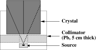
The sources were centered on one side about from the detector housing to illuminate both halves of the crystal equally (Fig 6). The -rays were collimated down to , using a thick lead shield. The source was mounted on a reproducible mount, to ensure that the relative source-detector position was always the same. A Hamamatsu R1513 PMT was optically coupled to the detector window using BCS 260 optical coupling grease. To study the effects of optical coupling quality on the overall detector efficiency two randomly chosen detectors were later used in conjunction with two other coupling methods, and the results were compared to those obtained here (see Section 3.3).
To extract the photoelectron yield, a plot of the two relative peak variances versus inverse peak-energy was made. A linear fit was made between the two points, using
Here is the zero-offset corrected peak mean. The slope of the line
was extracted from the fit and determines the number of photoelectrons per MeV
Here, is the Poisson distributed gain in the number of electrons produced at the PMT cathode which, for a stage Hamamatsu R1513 PMT operated at kV, is . The overall gain for the PMT used is at kV. The factor emerges due to the fluctuations in the number of electrons made at each dynode stage of the PMT, which contribute to the overall RMS width in the photopeaks. Corresponding to the activities of the two sources, the error in the yield due to counting statistics for the time counted are % for and % for . The overall error on the results is dominated by the quality of the least-squares fit.
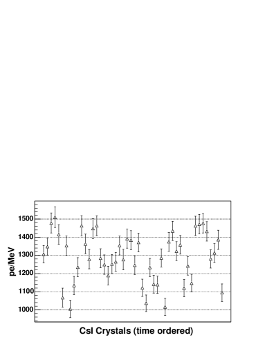
Possible gain nonuniformities from the two crystal halves were searched for by separately exposing each half to the source. Measurements were taken with the source on the left side, right side and the center of the scintillator, where the center is defined as seen in Fig. 6. In the worst case, the gain varies by about 7% from one crystal half to the other. The photoelectron yield measurements produced an average of 1300 photoelectrons per MeV with an overall variation of % between detectors. Figure 7 shows the results for 48 detectors in the order they were taken. The error in the values is about %, mostly due to the fitting procedure.
3.2 VPD Relative Gain and Efficiency
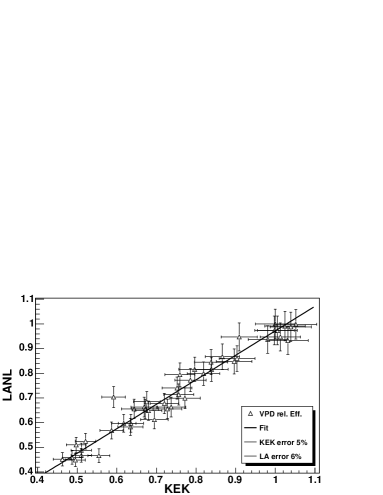
The response of the VPDs to the CsI scintillation is different from the response seen using a tungsten lamp, which was used by Hamamatsu Photonics to calibrate the VPDs. Therefore, it was decided that the VPD relative efficiencies had to be studied using the CsI scintillation light. The VPD efficiencies were measured using capture -rays from a neutron beam at KEK and relative efficiency measurements were performed at Los Alamos, using the LED’s in the detectors (see Section 3.2). At the pulsed epithermal neutron beam line at KEK, Cd and In targets were used to convert neutrons to -rays through radiative neutron capture at the Cd cutoff and at the In and resonances. One of the CsI crystals and its preamplifier were installed, together with each tested VPD, next to the target, using proper neutron and shielding. In this way, relative efficiencies of 57 VPDs were determined with an error of 6%. Comparisons of normalized VPD efficiencies at different neutron energies show a very high correlation, whereas the correlation between efficiencies measured with neutrons and those measured with a tungsten lamp is very poor [28].
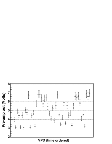
In a separate measurement the LEDs in each detector were used to establish the relative VPD efficiency again and verify the quality of the CsI-VPD gain matching. To measure the relative VPD efficiency, a single CsI crystal was coupled, in turn, with each VPD, using vacuum grease as coupling compound (see Section 3.3). A V, Hz square wave was applied to both LEDs in the detector. The current drawn by the LEDs was constant at mA throughout the measurement for 48 VPDs. The preamplifier output was monitored with a scope and with a precision voltmeter. The relative gains differ by up to a factor of 2.5. The results are shown in Fig. 8. A conservative estimate on the error in the efficiency is %, based on the fluctuations seen in the output of the precision voltmeter.
These measurements are compared with those done at KEK. Figure 9 shows that the results of the two independent measurements agree to within errors. The differences are most likely due to the change in optical coupling when switching the VPDs.
3.3 CsI to VPD Matching
As already mentioned, the CsI and VPD efficiencies are matched to reduce the overall gain variations in the detector array. However, fluctuations in the quality of the VPD-CsI optical coupling also affect the overall gain. A pair of detectors was tested with three optical coupling compounds:
-
1.
BC 630 Bicron optical coupling grease,
-
2.
Dow Corning Sylgard 184 Silicone Elastomer (cookies) and
-
3.
high vacuum grease (translucent).
The Sylgard elastomer was used to make “cookies”, circular mm diameter disks, about 3 mm thick. The initially liquid compound was pumped to remove air and cast into a mold standing on its side to make the surfaces as flat as possible. Unfortunately the compound was too hard and small nonuniformities on the VPD window or on the casting surfaces prevented the elastomer from producing a significant increase in coupling quality. The best results for the Sylgard elastomer are achieved by pouring it and allowing it to set in place, between scintillator and VPD. However, this option was not considered because the detector array configuration makes it difficult to exchange entire CsI-VPD assemblies in situ. The best efficiency results were obtained using optical coupling grease, which increased the gain by a factor of two over no coupling compound. However, BC 630 was disqualified due to its low viscosity and the vertical orientation of some of the VPD-CsI boundaries in the array. Since high vacuum grease is much more viscous and gave % of the gain of BC 630, it was chosen for the coupling.
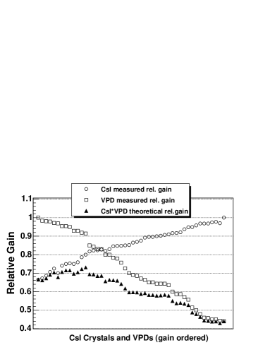
Figure 10 shows the gain ordered efficiency measurement results for the VPDs, the CsI crystals and their product. The curve showing the product of the efficiencies provides an upper limit on how well the gain of the detectors can be matched in hardware without further adjustments. The actual relative gain shifts are expected to differ from this prediction, due to variations in optical coupling quality among the detectors and variations in scintillation light response of the crystals over time. The CsI crystals were matched with the VPDs according to the efficiency results presented in Fig. 10. This selection served as a starting point from which to conduct additional efficiency measurements and further improve the gain via the adjustment of the feedback resistors in the detector preamplifier.
At this stage, all feedback resistance values in the preamplifiers (Fig. 3) were nominally identical for all detectors. The overall variation observed in the efficiency of the completely assembled detectors determine the change in feedback resistance necessary to adjust the gain in any given detector.
3.4 Combined Relative Detector Gain
To compare the predicted values of the relative gain between detectors, the assembled detectors were tested with a 137Cs source, intense enough to produce a current mode output. The corresponding preamplifier output was fed through a low-pass filter and monitored with a precision voltmeter. The source was located flush with the outside surface of the detectors and centered on one side. A source with the given activity (see Section 3.1) and in the given configuration (fractional solid angle is expected to deposit approximately into the detector. With the measured average CsI photoelectron yield of one expects to measure an output on the order of a few millivolts.
The low-pass filter was adjusted to have a time constant of 15 seconds to stabilize the voltage. Three measurements were taken for each detector, one without source, one with source in place, and again without the source. The measurements were performed quickly to avoid fluctuations with long time constants ( minutes). The mean voltage out of the preamplifier was 2.4 mV. Figure 11 shows the normalized difference between the signal with source and the average of the two signals taken without the source, versus detector number. The overall spread in gains is still %, but the relative gains shifted a bit, as expected.
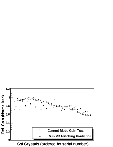
Resistors ranging from to were then installed in the second amplifier stage to reduce the gain variations. After adjusting the preamplifier resistors and assembling the detectors into the array stand (Fig. 1 for the final configuration), an additional set of data was taken to verify the final relative detector gains (before using the gain modules). This measurement was done, using a rotating 137Cs source and a lock in-amplifier. The source was located at the center of the ring corresponding to the detector that was tested. The reference phase for the lock in-amplifier was generated by an infrared emitter-receiver mounted onto the shaft of the rotating source. The measured normalized relative gains per detector are shown in Fig. 12. The lock in-amplifier and the rotating source were used to filter out noise and other fluctuations to obtain a cleaner measurement of the detector gains.
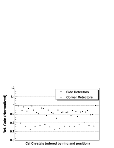
The corner detectors cover a solid angle that is % smaller than it is for the side detectors (Fig 1 and Fig 18). The gain in the corner detectors was then matched with the rest of the array by further adjusting their feedback resistors. This level of hardware gain matching is sufficient to prevent the difference channels from saturating.
The final precision of gain matching in the array will be limited by the quality of optical coupling as well as any time dependent gain fluctuations in the detectors. The next stage of gain matching will be implemented using custom built adjustable gain VME modules in the DAQ stream and will be performed during the commissioning run, in conjunction with a neutron beam and signals from neutron capture on a target. This work will be described elsewhere.
4 Noise Performance, Background and False Asymmetry Studies
In this section we describe studies of long term fluctuations in detector pedestals and electronic noise due to radioactive and electromagnetic background. We show that cosmic ray background in the detector array is understood and has no effect on the measured asymmetries. We discuss measurements performed to verify that false asymmetries due to electronic pickup and magnetic field induced gain changes in the VPDs are negligible.
These measurements required the acquisition of data over long periods of time and under conditions that are as close as possible to those encountered when the experiment is running. Accordingly, the entire array and spin flipper were assembled in their final configuration and data have been taken with the same DAQ setup to be used in the final experiment.
4.1 Detector Noise
The accuracy of the measurements described in this paper has to be viewed in relation to the noise levels in the detector pedestals.
In a current mode experiment, the accuracy of the measurement is governed by the rate and quality of sampling of a signal that may be viewed as a continuous string of values of a random variable. The randomness and the spread (RMS width) of the samples determine how many samples one must take to achieve a certain level of accuracy in the measurement, while the sampling rate determines how long that will take and whether or not one has in fact measured a representative subset of the signal. As the sampling rate is increased, a larger fraction of the width in the signal is due to the correlation between samples, and the observed error will be larger than expected from counting statistics. Thus, for a given number of samples taken, oversampling leads to loss in statistical information. Undersampling, on the other hand, will lead to information loss in the noise since high frequency fluctuations are aliased into lower frequencies.
The detector preamplifier (see section 2.2) and the rest of the DAQ were designed under the requirement that there be no substantial additional noise contribution beyond the expected Johnson noise from the resistors in the first preamplifier stage and the intrinsic noise of the operational amplifiers used [23]. To verify that this constraint has been met, it is important to consider the noise behavior one would expect based on the circuit design.
4.1.1 Expected Noise Performance
To establish the actual RMS width one expects to see in the voltage signal at the output of the preamplifier, one has to understand the origin of all noise contributions, their propagation through the DAQ and their final processing in the data stream. This includes determining a suitable sampling rate and the correct bandwidth for the predicted noise levels, set by the filtering in the DAQ.
For the purposes of noise analysis, the most important component of the preamplifier circuit (Fig 3) is the first stage connected to the VPD anode. This stage incorporates a feedback resistor () which is expected to completely dominate the noise. Subsequent resistors in the preamplifier and DAQ are smaller by three orders of magnitude and their noise contribution is thus negligible. However, each additional amplifier and filter stage will have a multiplicative effect on the noise generated in the first stage.
The thermal noise spectral density in the output of the first amplifier stage is predicted to be
| (3) |
Here is Boltzmann’s constant and is temperature.
A small addition to this noise density comes from the op-amp intrinsic noise. The total, Spice model666EECS Department of the University of California at Berkeley, http://bwrc.eecs.berkeley.edu/Classes/IcBook/SPICE/ predicted, RMS width in the current noise density for beam-off and LED off measurements is [23].
In the DAQ system, the signal from the preamplifier is processed by the sum and difference amplifiers, where it is fed through a six-pole Bessel filter with an average time constant (see Section 2.3, Fig. 4). The Bessel filter removes higher frequency noise components present in the preamplifier output [23]. This filtering has to take place before the digitization. The 16-bit ADCs do not have sufficient resolution to retain the full noise information at those frequencies and would cause aliasing of these components into lower frequencies. Further averaging in the data stream, after digitization, can not remove this noise without destroying the information content of the signal.
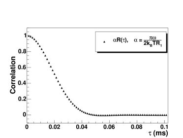
To find the expected RMS width at the output of the Bessel filter, one can calculate the corresponding auto-correlation function for the system [25, 29]. The effect of the Bessel filter can be calculated using the corresponding six-pole amplitude response function [30, 31]
| (4) |
where is a 6th order Bessel polynomial and is chosen such that the dc gain of the filter is unity. The correlation between time samples can then be calculated via
| (5) |
whereas the variance seen in an individual sample taken from the Bessel filter is given by
The graph shown in Fig. 13 is the result of a numerical integration of Eq. 5, for a range of intervals between samples.
Due to the Bessel filter, the values sampled by the ADCs are highly correlated at the sampling frequencies of kHz ( ms) or kHz ( ms) used in the DAQ, indicating that any high frequency components in the preamplifier output are filtered out. As a result of this oversampling, the variance for an individual time bin will be dominated by the correlation between samples.
Given the sampling scheme described in Section 2.3, the total variance for a time bin in the sum and difference signal is given by [25]
| (6) |
Here the correlation is given by Eq.(5), is the time difference between the initial sample and any subsequent sample taken during the sampling interval and is the total number of samples taken during the sampling interval.
In the calculation of the relevant statistic (mean, standard deviation, etc …), if we consider an individual time bin measurement as the fundamental random variable then ms, or , and will be the correlation between all ADC samples within that time bin. On the other hand, if we integrate over an entire macro pulse and consider that value to be the fundamental quantity then ms and will be the correlation between all ADC samples within that macro pulse and or . According to Fig. 13 any average value obtained for one time bin is essentially statistically independent from the value obtained for any other time bin. Taking either a time bin or an entire macro pulse as the fundamental quantity is therefore equivalent, provided that the measured signals have a distribution that is independent of time over the chosen interval. For beam-on measurements the signals observed in the detector array have a time dependence, because the neutron flux from the spallation source varies with neutron energy. The polarization of the neutrons as well as the capture distribution in the target are also energy (time) dependent. So in the measurement of an asymmetry from radiative neutron capture at a pulsed neutron source, it is necessary to select the time bin interval as the fundamental statistical quantity. The ms time bin width provides an energy resolution small enough to suppress the corresponding errors below the statistical limit [22].
Using the known values of the preamplifier resistors and the expected noise density from the first amplifier stage and taking a time bin as the sampling interval, Eq.(6) gives an expected RMS width at the preamplifier output of . The bandwidth is set by the Bessel filter time constants. For samples taken with ms, the second term in equation 6 evaluates to less than and increases by less than 1% when 25 samples are taken as is done for the sum channels. Gain factors multiplying the RMS width after the preamplifier are known and the width observed in the data can be related back to the noise at the preamplifier output. Other contributions to the noise introduced by the sum and difference amplifiers are negligible compared to the noise of the preamplifier.
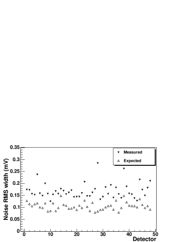
4.1.2 Noise Measurement Results
The RMS width of the noise is expected to be different for each detector due to the different feedback resistance values in each preamplifier (see section 3.4). The noise was measured with the data acquisition and the data were averaged over an 8 minute period. The noise seen in the detectors is shown in Fig. 14.
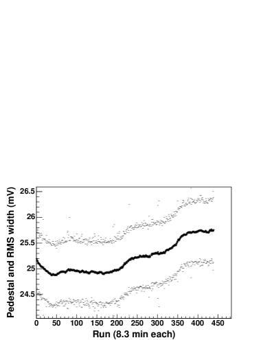
Detector pedestals and noise were monitored over a period of 60 hours. The pedestals were seen to drift by about mV on average and the noise RMS width stayed the same (Fig. 15).
The measured noise levels shown in Fig. 14 also include contributions from dark currents and cosmic ray background (See section 4.2), even after a 3 sigma cut to filter large cosmic ray signals. These contributions to the noise are not accounted for in the noise expected from the calculation above.
The measured RMS width in Fig. 15, on the other hand, includes all contributions to the noise and is observed to be a factor of 5 higher, on average, than the estimated noise level. These noise levels determine the time required to perform beam-off measurements of false asymmetries. During beam-on measurements, the expected shot noise RMS width is approximately mV, a factor of larger than the largest noise components for beam-off measurements.
4.2 Cosmic Ray Background
The detector signals seen during a pedestal run exhibit frequent sample outliers many standard deviations above the mean (see Fig. 5 and Fig. 16). These are due to cosmic rays incident on the detector array.
Considering the surface area of the detector array and its location, the number of cosmic muons that are expected to enter the array, per run, is on the order of a few times . This corresponds to detection of cosmics in less than % of the time bin samples taken in a given sampling period and a rate of about Hz in a single detector. Several measurements were performed to establish that the observed outliers do, in fact, correspond to cosmic radiation. These measurements used filtering techniques similar to those used on the L3 detector at CERN [32] and the SND detector at the Budker Institute for Nuclear Physics [33].
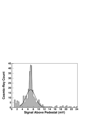
One of the measurements incorporated the use of cosmic ray event coincidences between a pair of detectors, one below the other. Two additional scintillator paddles were installed above and below the pair to trigger only those muons traversing the entire detector. For such events, the expected energy deposition is about MeV. Figure 17 shows the result, as obtained for the upper detector of a pair. According to the measured CsI photoelectron yield and the known detector gains, an instantaneous energy deposition of MeV should produce a signal, in one time bin, of approximately 7 mV above the pedestal mean.
4.3 False Asymmetries
In this section, we describe measurements performed to study systematic effects that may introduce false asymmetries as well as the time required to measure these effects (see Section 2.4).
The first measurement describes the tests for the sensitivity of the VPDs to AC and DC magnetic fields. The second measurement was done to establish the time required to average electronic noise down to the desired accuracy in the asymmetry. Here we essentially measured the asymmetry due to electronic noise, which is expected to be zero. This was done without operating any equipment other than the detector array itself and the DAQ. For the third measurement the RF spin flipper was operated and data were taken without any signal going into the detector array. This was done to search for an additive effect, in which an asymmetry may be induced as a result of an addition to the signal in the VPDs, due to spin flipper correlated electronic pickup. The fourth measurement looked for a multiplicative effect, a spin flipper correlated gain change in the VPDs, due to any spin flipper magnetic field leakage. This effect can only be seen by having a signal (light) going into the VPD, which was accomplished by using the LEDs in each detector so that the VPD current was approximately equal to that produced by the scintillation light expected during beam-on measurements.
4.3.1 VPD Magnetic Field Sensitivity
VPD gain can change due to magnetic fields interacting with the photoelectrons. This nonlinear effect increases with increasing current between cathode and anode. As already mentioned in section 2.4, if this effect is large, small fluctuations in the field could cause pulse-to-pulse variations in the detector signal and therefore produce false asymmetries. The sensitivity of the VPDs to magnetic fields was measured using both dc and ac fields.
An unshielded VPD connected to a preamplifier and a green LED were placed into a light-tight box which was located in a magnetic field up to G . The output of the preamplifier was monitored with a lock-in amplifier. The VPD was tested in a G dc field used in the experiment to control the neutron polarization and suppress Stern-Gerlach steering. The LED was pulsed at Hz and produced a mV peak-to-peak signal with various offsets up to V at the preamplifier output. The tests were performed with the VPD in parallel and perpendicular to the magnetic field direction as well as with the VPD rotated around its axis of symmetry. In each configuration, the change in gain for a dc field is only about . No gain dependence on the voltage offset was observed.
For the ac measurement, the LED was held at a constant voltage provided by a battery. The magnetic field was varied according to with G. The lock-in amplifier was used to measure first and second order changes in the gain and was synchronized to the field frequency. To first and second order the gain changes were and respectively [22]. The Aluminum housing normally placed around the VPD further reduces the coupling and for a pulse-to-pulse fluctuation of a few mG in the holding field the gain change in the VPD is negligible.
4.3.2 Asymmetry Definition
Given the vertical polarization direction of the neutrons in the NPDGamma experiment, the parity violating asymmetry is essentially seen in a difference of the number of -rays going up and down. For an asymmetry A, the -ray cross section is proportional to , where is the angle between the neutron polarization and the momentum of the emitted photon.
In calculating a false asymmetry, one asymmetry was calculated for each time bin and over any valid sequence of eight consecutive macro pulses (see Section 2.3) with the correct neutron spin state pattern. A valid 8-step sequence of spin states is defined as . This pattern suppresses first and second order gain drifts within the sequence.
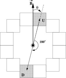
A pair of detectors is defined as shown in Fig. 18. If we let ( or ) denote the sum of all four signals with the corresponding spin states in a spin sequence, then the asymmetry for a time bin is given by
| (7) |
For the LED-on tests and beam-on data the denominator is given by the sum over all detector signals entering into the numerator of Eq.(7). For the beam-off, LED-off data the size of the denominator is set by the expected rate of -rays when the beam is on, as well as gain and sampling factors in the DAQ.
4.3.3 False Asymmetry Results
For the spin flipper on and off (no LED) asymmetry measurements, the time required to achieve a certain accuracy in the asymmetries is limited by the RMS width in the signal. As described above, the RMS width is set by the Johnson noise Eq.(6) and additional noise from the detector preamplifier [23] as well as cosmic ray and other background. The data were analyzed both with cuts to remove most of the cosmic-ray background and without cuts to study the influence of cosmic-rays on false asymmetries. The cuts were placed on the individual time bin samples and excluded samples larger than six times the noise width (6 sigma) seen in the pedestals.
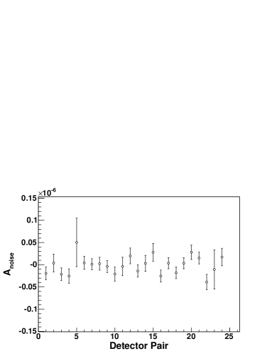
Many data runs contribute to the asymmetry measurements and for each detector pair in the array a combined mean and standard deviation were calculated from all runs. A total error-weighted average asymmetry is then calculated for the entire array. Without LEDs, the asymmetry can be measured down to the level in 3 hours. In 2 hours, the additive false asymmetry with the spin flipper was measured to
The individual detector pair asymmetries from the spin flipper runs are shown in Fig. 19. The noise observed in the detectors, with the spin flipper running, did not significantly change from the levels shown in Fig. 14. If no cuts are applied to remove the cosmic background, the time required to measure the noise asymmetry to the above accuracy increases by about a factor of five and the asymmetry is still consistent with zero. Table 1 shows the spin flipper on, LED off asymmetries for each ring in the detector array.
| Ring 1 | |
|---|---|
| Ring 2 | |
| Ring 3 | |
| Ring 4 |
With the LEDs turned on, the RMS width of the detector signals is dominated by shot noise at the photocathode. If the shot noise is characterized by a single electron, then the expected average noise density is at an average current of nA out of the VPDs. The multiplicative false asymmetry for the 24 detector pairs with LED signal is shown in Fig. 20.
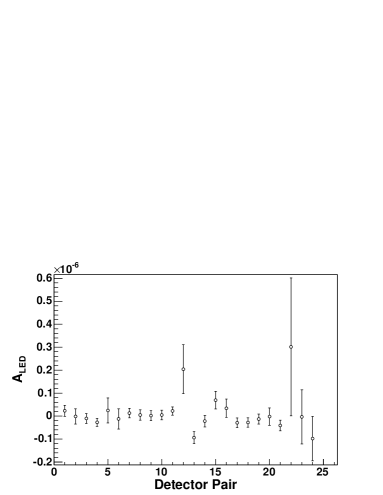
In 11 hours, the noise asymmetry with the LED signal, for the combined array, was measured to
| Ring 1 | |
|---|---|
| Ring 2 | |
| Ring 3 | |
| Ring 4 |
The noise in the detector preamplifier, as expected from calculation, predicts a run time estimate of hour to measure the beam-off, LED-off noise asymmetry to . From the estimate of the shot noise for LED-on measurements, the run time should be hours for an average photo-current of nA . The performed measurements show that the required run-times are actually 2 to 3 times larger than predicted. However, the average beam-off noise in the preamplifier, as seen in Fig. 14, is , about 70% higher than expected and the runtime required with this noise level corresponds to hours. The same was seen to be true for the LED-on (beam-on) measurement, where the noise observed was about 50% larger than expected from the above shot noise estimate.
5 Summary
The NPDGamma CsI(Tl) detector array has been designed and built to operate in current mode and at low noise without introducing instrumental systematic effects at the level. The prerequisite for a successful current mode measurement is the suppression of noise levels much below the statistical limit. The noise in the preamplifier due to thermal fluctuations in the circuit components was measured to be smaller, by a factor of 70, than the expected shot noise during measurements with a neutron beam. Since, in current mode detection, counting statistics appear as shot noise at the VPD photo-cathode, the accuracy of the asymmetry measurement will therefore be determined by counting statistics.
Any systematic false asymmetries arising due to the operation of the array and spin flipper must be suppressed to have an effect below . The beam-off, LED-off additive false asymmetry due to spin flipper correlated electronic pickup as well as the LED-on multiplicative false asymmetry due to spin flipper correlated gain changes in the VPD were measured to this level of accuracy within a few hours and were consistent with zero. These results show that the detector array is operating as designed and meets all criteria needed to perform a successful measurement of the weak parity-violating asymmetry with an accuracy of in the neutron capture reaction .
6 Acknowledgments
The authors would like to thank Mr. G. Peralta (LANL) for his technical support during this experiment, Mr. W. Fox (IUCF) and Mr. T. Ries (TRIUMF) for the mechanical design of the array and the construction of the stand and Mr. M. Kusner of Saint-Gobain in Newbury, Ohio for interactions during the manufacture and characterization of the CsI(Tl)crystals. We would also like to thank TRIUMF for providing the personnel and infrastructure for the stand construction. This work was supported in part by the U.S. Department of Energy (Office of Energy Research, under Contract W-7405-ENG-36), the National Science Foundation (Grant No. PHY-0100348) and the NSF Major Research Instrumentation program (NSF-0116146), the Natural Sciences and Engineering Research Council of Canada and the Japanese Grant-in-Aid for Scientific Research A12304014.
References
- [1] C. R. Gould, G. L. Greene, F. Plasil, and W. M. Snow, editors, Fundamental Physics with Pulsed Neutron Beams, World Scientific, ISBN 981-02-4667-6 (2001).
- [2] W. M. Snow, In the proceedings of the International Conference on Precision Measurements with Slow Neutrons, NIST Journal of Research (2004).
- [3] S. A. Page, et al., In the proceedings of the International Conference on Precision Measurements with Slow Neutrons, NIST Journal of Research (2004).
- [4] A. Komives, In the proceedings of the International Conference on Precision Measurements with Slow Neutrons, NIST Journal of Research (2004).
- [5] J. D. Bowman, et al., Measurement of the parity-violating gamma asymmetry in the capture of polarized cold neutrons by para-hydrogen, , Tech. Rep. LA-UR-99-5432, Los Alamos National Laboratory (1999).
- [6] W. M. Snow, et al., Nucl. Instr. Meth. A 440, (2000) 729.
- [7] W. M. Snow, et al., Nucl. Instr. Meth. A 515, (2003) 563.
- [8] B. Desplanques, J. F. Donoghue, B. R. Holstein, Annals of Physics 124, (1980) 449.
- [9] J. F. Briesmeister, ed., MCNP, A General Monte Carlo N-Particle Transport Code, Version 4C, LA-13709-M, Los Alamos National Laboratory (2000).
- [10] W. R. Nelson, H. Hirayama, D. W. O. Rogers, The EGS4 Code System, SLAC 265, SLAC, (1985).
- [11] R. E. MacFarlane, Technical Report No. LA-12146-C, Los Alamos National Laboratory (unpublished).
- [12] P.-N. Seo, et al., Nucl. Instr. Meth. A 517 (2004) 285.
- [13] H. Grassman, et al., Nucl. Instr. Meth. 228 (1985) 323.
- [14] P. Schotanus, et al., IEEE Trans. Nucl. Sci. 37 (1990) 177.
- [15] E. Frlez, B. K. Wright, D. Pocanic, Optics: General-Purpose Scintillator Light Response Simulation Code, Computer Physics Communications 0 (2000), 1-26.
- [16] G. F. Knoll, Radiation Detection and Measurement, John Wiley and Sons, New York, 1989.
- [17] D. Renker, Proceedings of the ECFA Study Week on Instrumentation for High-Luminosity Hadron Collider, (CERN, Geneva, 1989), Vol. CERN 89-10.
- [18] R. Zhu, Nucl. Instr. Meth. A 413 (1998) 297.
- [19] Z. Wei and R. Zhu, Nucl. Instr. Meth. A 326 (1993) 508.
- [20] M. A. H. Chowdhury and D. C. Imrie, Nucl. Instr. Meth. A 432 (1999) 138.
- [21] M. Kobayashi and S. Sakuragi, Nucl. Instr. Meth. A 254 (1987) 275.
- [22] G. S. Mitchell, et al., Nucl. Instr. Meth. A 521 (2004) 468.
- [23] W. S. Willburn, J. D. Bowman, M. T. Gericke, S. I. Penttilä, submitted to Nucl. Instr. Meth. A (2004).
- [24] M. T. Gericke, et al., In the proceedings of the International Conference on Precision Measurements with Slow Neutrons, NIST Journal of Research (2004).
- [25] W. B. Davenport, W. L. Root, An Introduction to the Theory of Random Signals and Noise, John Wiley & Sons, New York, 1987.
- [26] P. Horowitz, W. Hill, The Art of Electronics, Cambridge University Press, United Kingdom, 2001.
- [27] A. Csoto, B. F. Gibson and G. L. Payne, Phys. Rev. C 56 (1997) 631.
- [28] T. Ino, et al., Private communication.
- [29] J. D. Bowman and J. C. VanderLeeden, Nucl. Instr. Meth. 85 (1970) 19.
- [30] H. J. Blinchikoff, A. I. Zverev, Filtering in the Time and Frequency Domains, John Wiley & Sons, New York, 1976.
- [31] S. Winder, Filter Design, NEWNES Butterworth-Heinemann, Oxford, 1997.
- [32] J. A. Bakken, et al., Nucl. Instr. Meth. A 275 (1989) 81.
- [33] M. N. Achasov, et al., Nucl. Instr. Meth. A 401 (1997) 179.