[
Complex Dynamics of Piecewise Linear Model of the Van der Pol Oscillator
Under External Periodic Force
Abstract
The electronic model of Van der Pol oscillator with piecewise linear –characteristics of nonlinear element is proposed. It is carried out the experimental investigations of behaviour of the Van der Pol oscillator under external periodic force. The parameter plane ”the amplitude of external force – the frequency of external force” for the dynamical regimes of the oscillator is experimentally plotted. It is shown in experiments and numerical simulations that transition to chaos in the oscillator takes place through the period doubling cascade. It is revealed that the internal structure of the synchronization tongues has the characteristic view as for the crossroad area.
pacs:
PACS number(s): 05.45.+b]
The Van der Pol oscillator is a classical example of self-oscillatory system. More than seventy years after its appearing, the oscillator has become the main model self-oscillatory system with two dimensional phase space [1, 2, 3]. The classical experimental setup of the system is the oscillator with vacuum triode [2, 3]. The mathematical model for the system is well known second order ordinary differential equation with cubic nonlinearity – the Van der Pol equation. The Van der Pol equation is basic model for oscillatory processes in physics, electronics, biology, neurology, sociology and economics [4].
It was much attention dedicated to investigations of the peculiarities of the Van der Pol oscillator behaviour under external periodic (sinusoidal) force and, in particular, the synchronization phenomena and the dynamical chaos appearing (see e.g., [5, 6, 7, 8, 9]).
The investigations of the forced Van der Pol oscillator behaviour have carried out by many researchers. So, in 1927 Van der Pol and Van der Mark [1] in their investigations of the oscillator behaviour in the relaxation oscillation regime found that the subharmonical oscillations are appeared during changes of natural frequency of the system. Moreover, the authors noted appearing of ”irregular noise” before transition from one subharmonical regime to another. It seems to be it was one of the first observations of chaotic oscillations in the electronic circuit. Later, in 1945, Cartwright and Litlewood [10] during their analyzing the Van der Pol equation with large value of nonlinearity parameter have shown that the singular solutions exist. In 1949 Levinson [11], analytically analyzing the Van der Pol equation, substitutes the cubic nonlinearity for piecewise linear version and shows that the equation has singular solutions in the case also. It was revealed that chaotic behaviour is appeared in the Van der Pol equation with smooth nonlinearity by period doubling bifurcations [9] and crossroad area is observed in synchronization tongues [12].
However, up to the present day the difficulties connected with creation of the electronic model of the nonautonomous Van der Pol oscillator which demonstrates transition to chaos in physical experiment and will allows adequate numerical simulation are remained. The efficient enough way for creation of such kind models is building of the systems with piecewise linear voltage–current characteristics [13, 14]. In the paper [14] on the basis of numerical simulation shown that in piecewise linear model of sinusoidally forced Van der Pol oscillator the transition from periodic oscillations to chaotic ones is possible. The transition takes place through cascade of period doublings.
In this paper the results of experiment and numerical simulation of the sinosoidally forced Van der Pol oscillator model with symmetric piecewise linear voltage-current characteristic of nonlinear element are discussed.
Experimental circuit and models. The classical dimensionless form the nonautonomous Van der Pol oscillator is described by equation
| (1) |
where is the state variable, is the nonlinearity parameter, and are the amplitude and frequency of external force, respectively.
For building of electronic circuit of the Van der Pol oscillator which would be adequate for modeling by (1) the serial circuit could be used (Fig. 1a). The nonlinear element in the circuit (Fig. 1a) must obey with symmetrical characteristics with negative resistance region. The nonlinear resistor with three-segment piecewise linear –type voltage-current characteristic is created on an operation amplifier [15]. The scheme is shown in Fig. 1b, where the rest parameters are R1=R3=3.6 k, R2=400 , V, V. The voltage-current characteristic measured in experiment for the above mentioned parameter values is presented in Fig. 2. The resistance at negative region of nonlinear element voltage-current characteristic is and at positive region is .
On the basis of Kirhgoff laws the equations for the Van der Pol oscillator model (Fig. 1a) could be written as
| (2) | |||||
| (3) |
where is the voltage at the inductor, is the voltage at the resistor, is the voltage at the capacitor, is the function describing piecewise linear voltage–current characteristic of the nonlinear element ””, and are the amplitude and frequency of external force, respectively. Introducing new dimensionless quantities: , , , , , , , , in term of which (2) become
| (4) | |||||
| (5) |
where and are the values of current and voltage in extremum of the voltage-current characteristic (Fig. 2), .


Along with the piecewise linear form of in the equations (4) the arbitrary function could be used. So, if nonlinearity in eqs. (4) is governed by then additive ”” could be removed by rescaling and finally the eq. (1) is obtained. Thus, the experimental scheme (Fig. 1a) and the appropriate equation (4) are adequately described the classical Van der Pol oscillator under external force (1).

Experimental results. For systems under external force, as a rule, the synchronization phenomena of the natural oscillations by external periodical force are investigated at the parameter plane ”the amplitude – the frequency of external force”. Most frequently the synchronization regimes are marked by (1:1), (1:2), (1:3) and so on. Such notations of the synchronization regimes show the relation of the natural frequency of gerenator’s oscillations () to the frequency of the external force (). There are so called main synchronization regimes marked by (1:1), (1:2), (1:3), (3:1), (2:1) etc. Between such regimes the more complicated multiloop regimes of high order are placed. All these regimes have the rational relation of frequencies. Moreover, the regions (quasiperiodical oscillations) with irrational relation of frequencies exist.
Experimental investigation of the driven Van der Pol oscillator behaviour is in plotting of synchronization regimes at the parameter plane. For experiments in this work the following parameters were used: =25.8 , =83.5 nF, =4.37 mH (Fig. 1a). The resistance is total resistance (excluding , =23.3 is the resistance of inductor) of the circuit. The boundaries of oscillatory regimes were defined from the phase portrait view during the changes of controlling parameters. In the some cases the changing of both parameters simultaneously is needed because the oscillator demonstrates the multistable behaviour. The multistability is appeared as existence of the histeresis boundaries for different oscillatory regimes. It could be proposed there are the regions which could be reached for the both parameter changing only.
When the parameter plane has been plotted the synchronization regimes were identified by phase portraits. The different regimes depicted as the synchronization tongues. Generally speaking, the tongues of higher order are placed under the tongues of the lower order, for example, the synchronization tongue (1:2) could be partially placed under the synchronization tongue (1:1). The regions with period doubling is marked with subscript letters (e.g., , ), the regions with chaotic behaviour is marked with subscript (e.g., (1:2).
The parameter plane ”the amplitude – the frequency of external force” for the Van der Pol oscillator (Fig. 1) with the piecewise-linear ––characteristics of nonlinearity (Fig. 2) is shown in Fig. 3. The main synchronization tongues are shown in Fig. 3 only, although, many narrow tongues with rational frequencies relation are observed in experiment. The phase portraits for typical dynamical regimes depicted at the parameter plane (Fig. 3) are shown in Fig. 4. In Fig. 4 the amplitude of external force changes for the horizontal axis and the voltage in the point of connection of capacitor and inductor – for vertical axis. The data were sampled with an analog to digital converter with 8–bit resolution at sampling rate samples per second, the length of time series is 3000 points.

As it is seen in Fig. 3 the overlapping of the synchronization tongues (1:2) and (1:3) in the vicinity kHz, V takes place. The chaotic regimes with strange attractor could be seen in the synchronization tongues (1:2) and (1:4), more precisely in , regions. It is easily seen that the internal structure of the synchronization tongue (1:4) has the view that is characteristic for the bifurcation composition called crossroad area [16].
Numerical simulation. In the numerical simulation of the driven Van der Pol oscillator with piecewise-linear characteristic the dimensionless form of equations (4) is used. The voltage-current characteristic of the nonlinear element (Fig. 2) is transformed to dimensionless form also (Fig. 5). The analytical form of piecewise-linear ––characteristic could be described by equation
| (6) |
Taking into account the values of the characteristic scales of the piecewise linear nonlinearity ( mA, V) and the values of the circuit elements (Fig. 1) the dimensionless parameters (, ) of the system (4) are calculated.


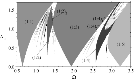
The parameter plane ”the amplitude – the frequency of external force” for the system (4) with piecewise-linear characteristic (6) obtained in numerical simulation is shown in Fig. 6, where synchronization regions are marked in gray scale. For plotting of the parameter plane (Fig. 6) the system (4), (6) was integrated by using of the fourth order Runge-Kutta method with constant time step . The identification of the synchronization regime was carried out from Poincare section by selecting points in the section through the period of the external force.
It is seen from Fig. 6, that the characteristic synchronization tongues are obtained. Main synchronization tongues are marked, besides, many synchronization tongues of higher order are also visible. The route to chaos via period doublings is observed within the synchronization tongues (1:2) and (1:4). Moreover, the view of the internal structure of the synchronization tongues (1:2) and (1:4) allows to conclude that the crossroad area takes place in a similar way as it was found in natural experiments with the electronic circuit (Fig. 1).
The visual comparison of the parameter planes obtained in the natural experiment and the numerical simulation (Fig. 3 and 6, respectively) leads to conclusion about qualitative agreement of both experiment and simulation. The further comparisons could be done if to rescale the experimental results (Fig. 3) to numerical simulated ones (Fig. 6) using the coefficients introduced for obtaining the dimensionless equation (4) then it is seen the good quantitative agreement of both experiment and simulation.

Conclusion. In this paper the electronic model of the Van der Pol oscillator with piecewise linear characteristic of nonlinear element is proposed. It is discussed results of the experiment on the investigation of the oscillator behaviour under external sinusoidal force at the parameter plane ”the amplitude – the frequency of external force”. The primary attention has been paid to the revealing of regions on the parameter plane in which the chaotic behaviour is realized and to investigations of internal structure of such regions. It is shown that transition to chaos via period doubling is taken place within the synchronization tongues (1:2) and (1:4) (here ratio of natural frequency of oscillator to external force frequency) as well as in many synchronization tongues of higher order.
The comparison of the parameter planes obtained in experiment and numerical simulation showed that the planes obey with both qualitative and quantitative similarity for boundaries of regions with synchronous and chaotic behaviour. To demonstrate this fact the typical points from the experimental parameter plane (Fig. 3) could be rescaled to dimensionless case and compared with the same points for the parameter plane obtained in numerical simulation (Fig. 6). So, for the point ( kHz, V) of minimum for at the boundary of (1:2) and (1:2)2 regimes (Fig. 3) could be calculated dimensionless values (, ) that in good agreement with the point of minimum for at the same boundary (Fig. 6), analogously, for the point ( kHz, V) of minimum at the boundary (1:4)2 and (1:4)4 is obtained (, ). The region at the parameter plane where transition to chaos takes place is displaced within the synchronization tongues (1:2) and (1:4). The region has the crossroad area like view. The results of experimental investigations and numerical simulations of the changes of the parameter plane structure for large values of external force and the circuit elements will be published elsewhere.
This work was partially supported by the RFBR under grant No.02–02–16351, the Ministry of Education of RF under grant No.E02–3.5–149 and the CRDF (BRHE REC–006).
REFERENCES
- [1] B. Van der Pol and J. Van der Mark, Nature 120, 363 (1927).
- [2] A.A. Andronov, A.A. Vitt, and S.E. Khaikin, Theory of Oscillators (Pergamon Press, London, 1966).
- [3] M.I. Rabinovich and D.I. Trubetskov, Oscillations and Waves in Linear and Nonlinear Systems (Kluwer, Netherlands, 1989).
- [4] W. Ebeling, Structurbilding bei Irreversiblen Prozessen (Leipzig, 1976); L. Glass and M.C. Mackey, From Clocks to Chaos. The Rhythms of Life (Princeton University Press, Princeton, 1988); H.G. Schuster, Deterministic Chaos: An Introduction (VCH, Weinheim, 1988); W.-B. Zhang, Synergetic Economics (Springer-Verlag, Berlin Heidelberg, 1991); V.S. Anishchenko, Dynamical Chaos – Models and Experiments (World Scientific, Singapore, 1995); H.D.I. Abarbanel, M.I. Rabinovich, A. Selverston, M.V. Bazhenov, R. Huerta, M.M. Sushchik, and L.L.Rubchinskii, Phys. Usp. 39, 337 (1996).
- [5] J. Guckenheimer, IEEE Trans. Circuits Syst. 27, 983 (1980).
- [6] M.P. Kennedy and L.O. Chua, IEEE Trans. Circuits Syst. 33, 974 (1986).
- [7] Y. Ueda and N. Akamatsu, IEEE Trans. Circuits Syst. 28, 217 (1981).
- [8] G.R. Qin, D.C. Gong, and X.D. Wen, Phys. Lett. A 141, 412 (1989).
- [9] U. Parlitz and W. Lauterborn, Phys. Rev. A 36, 1428 (1987).
- [10] M.L. Cartwright and J.E. Litlewood, J. London Math. Soc. 20, 180 (1945).
- [11] N. Levinson, Ann. Math. 50, 127 (1949).
- [12] R. Mettin, U. Parlitz, and W. Lauterborn, Int. J. Bifurc. Chaos 3, 1529 (1993).
- [13] T. Matsumoto, L.O. Chua, and M. Komuro, IEEE Trans. Circuits Syst. 32, 798 (1985).
- [14] E.S. Mchedlova, in the Proceedings of the 5th International Specialist Workshop on Nonlinear Dynamics of Electronic Systems (NDES–97) (Moscow, Russia, June 26–27, 1997) (Moscow, 1997), p.449–452.
- [15] L.O. Chua, C. Desoer, and E. Kuh, Linear and Nonlinear Circuits (McGrow–Hill Book Company, 1987).
- [16] J.P. Carcasses, C. Mira, M. Bosch, C. Simo, and J.C. Tatjer, Int. J. Bifurc. Chaos 1, 183 (1991); A.P. Kuznetsov, S.P. Kuznetsov, and I.R. Sataev, Izvestiya VUZov. Prikladnaya Nelineynaya Dinamika. 1 (3/4), 17 (1993) (in Russian).