Unified Model, and Novel Reverse Recovery Nonlinearities, of the Driven Diode Resonator
Abstract
We study the origins of period doubling and chaos in the driven series resistor-inductor-varactor diode (RLD) nonlinear resonant circuit. We find that resonators driven at frequencies much higher than the diode reverse recovery rate do not show period doubling. Models of chaos based on the nonlinear capacitance of the varactor diode display a reverse-recovery-like effect, and this effect strongly resembles reverse recovery of real diodes. We find for the first time that in addition to the known dependence of the reverse recovery time on past current maxima, there are also important nonlinear dependencies on pulse frequency, duty-cycle, and DC voltage bias. Similar nonlinearities are present in the nonlinear capacitance models of these diodes. We conclude that a history-dependent and nonlinear reverse recovery time is an essential ingredient for chaotic behavior of this circuit, and demonstrate for the first time that all major competing models have this effect, either explicitly or implicitly. Besides unifying the two major models of RLD chaos, our work reveals that the nonlinearities of the reverse recovery time must be included for a complete understanding of period doubling and chaos in this circuit.
I Introduction
The nonlinear dynamics of the p-n junction has been a subject of intense interest since the dawn of chaos.[1, 2, 3, 4, 5, 6, 7, 8] Experimental work has focused on the damped driven nonlinear oscillator formed by a resistor, inductor, and varactor diode (RLD circuit) connected in series (see Fig. 1(a)). This is the simplest passive circuit that displays period doubling and chaos as a function of sinusoidal driving amplitude and frequency. The dynamics of this circuit can, in principle, be understood through the details of the hole and electron charge distributions in the vicinity of the p-n junction.[9] However, many simplified models of p-n junction charge dynamics have been put forward in terms of nonlinear lumped-element approximations for the varactor (Fig. 1(b)). One reason for this approach was the interest in constructing low-dimensional maps to describe the ”universal” nonlinear dynamics experimentally observed in the circuit.[1, 2, 4, 6]
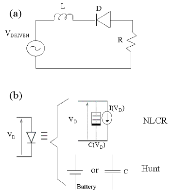
There are three general types of nonlinearity present in the driven RLD circuit. The first is the nonlinear current-voltage characteristic of the diode, thought by most researchers to be unimportant for chaos, because its absence from models results in only small changes in the calculated bifurcation diagrams.[5, 10] A second contribution comes from the large and exponentially nonlinear forward-bias capacitance associated with the junction diffusion capacitance.[5] In this case, the diode is modeled as a parallel combination of a nonlinear resistor and nonlinear capacitor (Fig. 1 (b)). It has been proposed that period doubling will occur when the capacitance reaches approximately four times its zero bias value because the resonant frequency of the RLD circuit will drop to half its low-amplitude value.[7] This is thought to be the first step in a period doubling cascade to chaos. A third contribution to nonlinearity comes from the finite time-scale diffusive dynamics of charge in the p-n junction and the associated ”memory” of previous forward-current maxima.[4] After the diode has been forward-biased and switched off, it takes some time for the minority carriers to diffuse back across the junction, allowing the diode to conduct for a period known as the reverse-recovery time, . The ”memory” of previous forward bias currents built into this non-equilibrium charge distribution has been proposed as the main source of chaos in the driven RLD circuit.[4, 8]
Lumped element models of the driven RLD circuit fall into two distinct classes: those relying on the nonlinear capacitance and ignoring explicit history effects (Fig. 1(b) NLCR), and those explicitly based on history effects in the junction and ignoring the nonlinear capacitance (Fig. 1(b) Hunt). Both kinds of model attempt to identify the essential physics that is responsible for period doubling and chaos. It is remarkable that both classes of models reproduce intricate detail of the return maps and bifurcation diagrams of the driven RLD circuit. Historically, the two classes of models were assumed to be mutually exclusive and contradictory in their approach to describing chaotic dynamics in the driven RLD circuit.[11] One purpose of this paper is to partially reconcile these two classes of models, and to show that they both include some essential physics of this rich nonlinear problem. We also demonstrate that both models lack important effects that have been ignored up to this point. These effects are measured here for the first time in the context of nonlinear dynamics, and are essential for a complete understanding of the behavior of this circuit.
In this paper we present new measurements and simulations of reverse-recovery times in a variety of diodes and resonant circuits. Section II discusses the many time scales of the driven RLD problem and illustrates the importance of the reverse recovery time in the nonlinear dynamics of the circuit. Section III demonstrates that the nonlinear capacitance models are endowed with a history-dependent reverse-recovery-like effect. Section IV is a summary of our experimental results of the nonlinear dependence of the reverse recovery time on circuit parameters, and ends with a dramatic illustration of how existing models fail to explain key data. Sections V and VI review our contributions to a deeper understanding of the RLD circuit and demonstrate that a simple nonlinear capacitor model shows all of the essential features of reverse-recovery-like behavior.
Experiments were carried out in a manner similar to that described in Ref. [12]. The circuits were shielded inside a metallic box and excited through 50 transmission lines by either an HP 33120A synthesized source (up to 15 MHz) or an HP 83620B microwave synthesizer (above 10 MHz). The response of the circuits was measured with either a Tektronix TDS3052 oscilloscope, or a Tektronix 494P spectrum analyzer. Low capacitance and high impedance probes were used to measure voltages in the circuits. SPICE simulations showed that the probes had a minimal impact on the circuit waveforms, whereas it was found that low impedance capacitive probes strongly perturbed the circuits. Bifurcation diagrams were constructed by collecting single-shot traces from the oscilloscope and recording the data with a LabView program on a PC.
II Time Scales
The history of research on the driven RLD circuit is long and varied. Most papers on this subject study only one diode and choose a circuit with a resonant frequency in a convenient range (typically at audio frequencies). The experiments have been carried out in widely disparate regions of the parameter space available for the circuit (the parameters include driving frequency, amplitude, and duty-cycle, R and L values, minority carrier lifetime, dc voltage bias, etc.).[13, 14, 15, 16, 17] Only recently has effort been made to assemble a unifying picture of the origins and generality of period doubling and chaos in this important circuit.[10] Our purpose in this section is to measure and model different diode circuits in a wide range of parameter space to identify the important and essential physics responsible for the nonlinear dynamics of the driven RLD circuit as a step in creating such a unified picture.
It is important to first understand the four major time/frequency scales involved in this problem, because the dynamics of the circuit depends critically on the relative values of these time scales. The first is the low-amplitude resonant frequency of the passive RLD circuit: f0 = 1/[2(LCj)1/2], where Cj is the zero-bias junction capacitance of the varactor diode. It is well established that complex dynamics are most easily observed for driving frequencies f in the vicinity of this resonant frequency. Another important time scale in the diode is the reverse recovery time: . This is a measure of the time required for minority carriers injected across the junction in the diode to move back to the other side of the junction (or recombine) once the driving force has been removed. One effect of this finite time scale is ”reverse recovery” in which a forward-biased diode will not shut off immediately when the driving signal is reversed, but will continue to conduct for a time on the order of . Su, Rollins and Hunt proposed that the diode actually acts like a battery during this time. In addition, they proposed that retained a memory of the two or three previous maximum forward current values through the diode.[8]
There are several RC time constants in the problem, associated with the junction capacitance and the internal resistance of the diode, and between the junction capacitance and the external resistor, R (note that the parasitic resistance of the inductor is much less than R for the circuits considered here). These time scales are usually quite short ( ns), but can be important when the capacitance is large. Finally, the L/R time scale is generally long and does not directly influence the diode dynamics. The interplay of these time scales, along with the period of the sinusoidal driving signal, yield a very rich parameteric landscape for nonlinear dynamics.
It should be mentioned that three of these time scales are strongly nonlinear. The resonant frequency f0 and the RC time constants are a nonlinear function of driving amplitude and DC voltage bias on the varactor junction, and we show for the first time below, the reverse recovery time is a nonlinear function of drive frequency, amplitude, duty-cycle, DC bias, and load resistance.[9] Most of these nonlinearities have not been investigated in the past with respect to the resulting nonlinear dynamics. These nonlinearities greatly enrich the dynamics and challenge our understanding of the essential physics responsible for nonlinear dynamics in the simple driven RLD circuit.
To illustrate the interplay of time scales in this problem, consider the sinusoidally driven resonant RLD circuit shown in Fig. 1(a). The low-amplitude resonant frequency of the circuit is determined by the diode junction capacitance Cj as well as the lumped element inductor, L. The reverse recovery time can be measured by methods discussed below. We studied four different diodes with very different values of Cj and . In all cases we find the following. First, when the low-amplitude resonant frequency of the circuit f0 is on the order of 1/, period doubling and chaos are found for a substantial driving frequency range f between about 0.2 f0 and 2 f0 (see Table I). Similar results are obtained when the inductance is changed to make the resonant frequency equal to about one tenth of 1/ (in agreement with Ref. [10]). However, when the inductance is changed to make f0 about ten times larger than 1/, there is a substantial change in the circuit behavior (Table I). One of the diode circuits shows only period doubling and no chaos, while another displays nothing but period-one behavior. The other diode circuits show period doubling and chaos, but over a more restricted range of amplitude and driving frequency parameter space. Finally, when the circuits are modified to have f0 100/, we do not observe period doubling or chaos at all over the equivalent range of parameters.
When the diode is driven at frequencies much higher than the reverse recovery time, the charge carriers near the p-n junction do not have a chance to influence the circuit behavior or contribute additional nonlinear behavior. Clearly the reverse recovery time plays an important role in the nonlinear dynamics of this circuit. However, very little prior experimental work on RLD dynamics has explored the interplay of all the time scales in this problem.
III The Storage () and Reverse Recovery () Time Scales
Hunt and collaborators claimed that the reverse recovery time is the key feature that generates chaos in the driven RLD circuit because it is a function of the peak current flow in previous cycles, thus introducing a memory effect into the dynamics. In the paper by Rollins and Hunt [4] a simple model of reverse recovery was introduced for RLD dynamics, and turned into a 1D noninvertible map. Although this gave qualitative agreement with experiment, it was criticized for being inconsistent with the measured attractor.[5] Later, Su, Rollins and Hunt [8] included three or more previous cycles of the forward bias current to determine their model . They also noted that the recovery time depends on the junction characteristics and the external series resistance. We show here that this model is a good starting point, but fails to include essential nonlinearities.
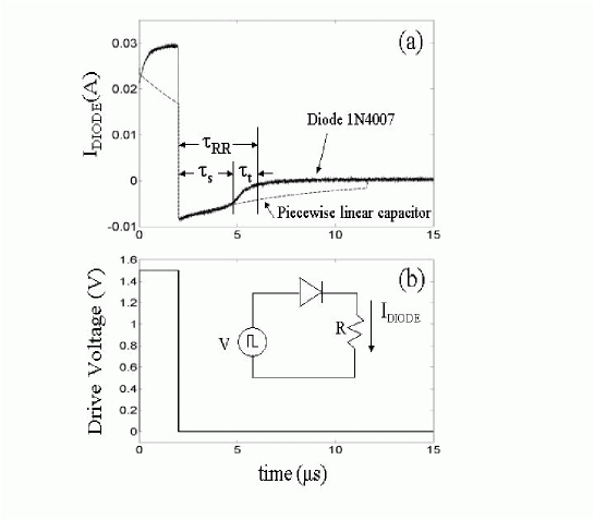
Figure 2 illustrates the reverse recovery effect in a diode. The circuit shown in the inset of Fig. 2(b) was employed to drive the diode with a single square pulse input. After the driving signal was removed, the diode continued to conduct for a time scale defined as the reverse recovery time, . This time consists of two contributions: the storage time , and the transition time , with = + .[9] We shall present results below (all data in Figs. 3 - 7 are taken with the circuit shown in Fig. 2(b)) mainly on the storage time because, in general, this time scale dominates the reverse recovery time and its nonlinear behavior.
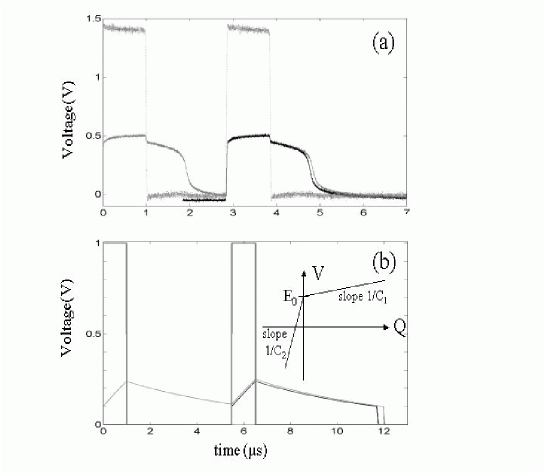
Figure 3 illustrates the history dependence of the storage and reverse recovery times. In this case we compare single pulse recovery data like that shown in Fig. 2 to the same diode subjected to two consecutive pulses (Fig. 3(a)). The storage time is longer for the diode that has been subjected to two pulses, mainly because it was not finished recovering from the first pulse before the second arrives. This simple history dependence of the recovery time is the basis for the Hunt and Rollins treatment of complex RLD dynamics.[4, 18]
All other models of RLD dynamics do not consider an explicit history dependence of the junction dynamics of the diode. They are based on the nonlinear behavior of the capacitor used to approximate the reactive electrical behavior of the diode (Fig. 1(b), NLCR). As we shall show here, in fact all of these other models do indeed have a history-dependence of a reverse-recovery-like time that naturally comes from the charge storage on the capacitor part of the varactor diode model.
A Piece-wise Linear Capacitor (PLC) Model
To illustrate our point, we shall choose the simplest model of the nonlinear capacitance in the varactor. In this case, one can use a piece-wise linear approximation for the capacitance of the varactor, with just two linear pieces. This model for the varactor capacitance was considered by several groups[6, 19, 20] and shown to produce period doubling and chaos when part of an R-L-PLC series circuit driven by a sinusoidal signal. The inset to Fig. 3(b) shows that the PLC switches at potential E0 from a large value C1 for higher bias, to a small value C2 for lower bias. We use this model to illustrate that it has implicitly included a history-dependent storage time. Fig. 2(a) shows a SPICE simulation of the diode current (dashed line) using the PLC model for the varactor in the circuit shown in the inset of Fig. 2(b), where the diode is replaced with the PLC. It clearly displays a ”storage time” and a ”transition time”, just like a real diode.[21] The ”storage time” () in this case corresponds to the RC time constant of the capacitor discharging into the external resistance of the circuit while it has a large capacitance C1. The ”transition” part of the signal occurs when the device switches to its smaller capacitance value C2, producing a much shorter RC time constant that discharges the capacitor very quickly. Thus the discharge behavior of the capacitor mimics the effects of minority charge carrier diffusion across the junction. As we shall see, the details of this discharge behavior are remarkably similar to the diffusive dynamics of the minority charges in real diodes.
We have found that a variety of models based on nonlinear capacitance of the diode show a history dependence of the RC storage and ”reverse recovery” times. Fig. 3(b) illustrates the history-dependence of the RC discharge time in the PLC model. All models of RLD dynamics that we have investigated have a history-dependent reverse recovery effect coming from the nonlinear capacitance. Our conclusion is that a finite reverse recovery time is indeed an important concept for understanding chaos in this circuit. Besides making this point in this paper, we also wish to explore the nonlinear and history-dependent behavior of this recovery time and how it influences the generic behavior of the driven RLD circuit.
IV Nonlinear Behavior of the Storage Time
The storage time and its history dependence are clearly important ingredients in any model of nonlinear dynamics of the driven RLD circuit. However, it is not widely appreciated that the storage time is itself a strongly nonlinear function of many parameters in the problem. These parameters include the amplitude of the forward bias current, the circuit resistance R, the driving frequency, the duty cycle of the drive, and the DC voltage bias on the junction. The purpose of this section is to present experimental evidence and models of these nonlinearities and to discuss their significance for the occurrence of period doubling and chaos in the parameter space of these circuits.
First is the forward current amplitude dependence of the storage time . Hunt and Rollins pointed out that the reverse recovery time of a diode increases as the amplitude of the forward bias current through the diode increases. The approximate expression used to describe this effect was;[4, 18]
| (1) |
where Imax is the most recent maximum forward current, and Ic are lifetime and current scales particular to each diode. A more exact expression for the storage time can be derived from analysis of charge dynamics in the p-n junction;[22]
| (2) |
that can be approximated as;
| (3) |
where IR is the reverse current through the diode during the storage phase. All of these forms basically say that the storage and reverse recovery times will increase as the amplitude of the forward current increases. This is because more minority charge will be pushed across the junction by the larger current and, because of the diffusive dynamics of the carriers, there will be a longer delay in getting back to the equilibrium charge configuration.
Data and PSpice simulations for the forward current dependence of the storage time in two different diodes is shown in Fig. 4. (Note that PSpice simulations use standardized semi-empirical models of the diode behavior, while our SPICE simulations of the PLC use the model shown in the inset of Fig. 3(b) with parameters given in the caption of Fig. 2.) The circuit in the inset of Fig. 2(b) was used to perform these measurements and simulations. For the data in Figs. 4 and 5 the driving signal is a periodic square wave with an equal time spent at the positive and negative amplitude voltage values (50% duty cycle). The storage time was measured as a function of the driving signal amplitude, proportional to the forward current through the diode. The data and simulations all show an increase of the storage time with increased forward bias current. In some cases the storage time saturates, consistent with the approximate expression Eq. (1), and in other cases it continues to rise slowly, consistent with the more sophisticated treatment in Eqs. (2) and (3).
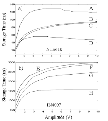
It has also been noted that the value of the resistance R in the circuit of Fig. 2(b) (and therefore Fig. 1(a)) will also influence the storage and reverse recovery times.[8, 18] This is illustrated in Fig. 4. When the load resistance R is changed from 25 to 1 k, the storage time increases for both diodes (NTE610 and 1N4007) in both experiment and simulation. This is expected because the reverse recovery process involves charge transport across the junction and through the rest of the circuit. A larger external resistance in the circuit will imply a smaller reverse recovery current, thus extending the time for the minority charge to re-establish its equilibrium configuration. Note that a similar effect will occur in models of nonlinear capacitance. In that case the discharge time of the capacitor is an RC time constant, which clearly grows with external resistance R.[23]
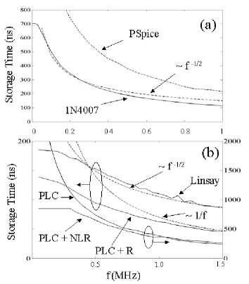
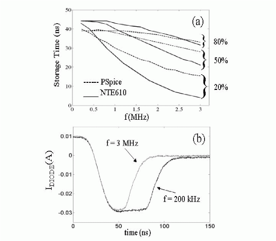
The nonlinearities of the storage time dependence on forward bias current and resistance have been noticed in the past. However, we are not aware of any group noting the following nonlinearity in the reverse recovery time. When the circuit in the inset of Fig. 2(b) is used with a repetitive square wave pulse sequence, one finds a strong dependence of the reverse recovery time on the pulse frequency. We consider the case where the pulses remain sufficiently far apart that the diode appears to fully recover from the previous pulse before the next arrives. As the rate of pulsing increases, the recovery time dramatically decreases. The effect is illustrated in Figs. 5 and 6. Fig. 6(b) shows recovery traces from an NTE610 diode at two pulse frequencies. With a pulse repetition rate of 200 kHz, the storage time is about 40 ns, while at a repetition rate of 3 MHz it has decreased to less than 20 ns. Figs. 5 and 6 show that in general the storage time is constant at low frequencies, and then begins to fall roughly like f-1/2 with increasing frequency. This behavior is seen in both experiment and PSpice simulation of the 1N4002, NTE610, and Linsay[1] model diodes.
From examination of charge dynamics in the p-n junction it is known that the diffusion capacitance CD is a function of frequency for sinusoidal driving signals;[9]
| (4) |
where g is the differential conductance of the diode g = dI/dV. The f-1/2 frequency dependence of the capacitance comes from the diffusive nature of charge transport in the junction region.[9] The diffusion capacitance diminishes with increasing frequency beyond f 1/2, resulting in less charge stored in the p-n junction for a given forward bias current. This in turn implies that less minority carrier charge must be moved across the junction at high frequencies, resulting in a shorter storage and reverse recovery time. This is consistent with the results presented in Figures 5 and 6 for two rather different diodes (1N4007 and NTE610).
One possible consequence of the frequency-dependent storage time is the persistence of period doubling behavior to unexpectedly high frequencies in the driven RLD circuit. As the driving frequency increases, the diffusion capacitance and storage time decrease, effectively increasing both the resonant frequency f0 and 1/. This nonlinearity essentially helps to maintain the condition f f0 1/ (where period doubling and chaos is most easily observed) over an extended range of driving frequencies. Thus period doubling and chaotic behavior should be more robust in the driven RLD circuit than one might naively expect.
Fig. 6(a) illustrates the duty-cycle dependence of the storage time and its frequency dependence. The duty cycle is defined as the ratio of the time spent at the positive amplitude voltage value to the total period of the periodic square pulse signal. As the duty cycle increases, there is greater overlap between adjacent pulses, causing the enhancement of the reverse recovery time, as originally noted by Hunt and collaborators and summarized in Eqs. (1)-(3). Again we see very consistent behavior in both experiment and PSpice simulations.
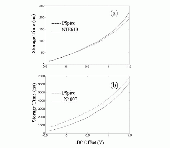
Finally, we have noted a strong DC voltage bias dependence of the storage time. The data and simulations on two different diodes is shown in Fig. 7. For forward bias the storage time increases dramatically, while for negative bias it decreases. The range of storage time variation is more than a factor of 10 for a 2 volt swing in DC bias voltage. A forward-biased diode will have a broader region of minority charge distribution, forcing the carriers to travel greater distances. This in turn increases the recovery time of the diode. Similarly, a reverse biased diode is able to sweep the minority carriers across the junction more quickly with the additional driving force provided by the reverse DC bias. This strong nonlinearity of the recovery time has not been discussed in the nonlinear dynamics literature, to our knowledge.
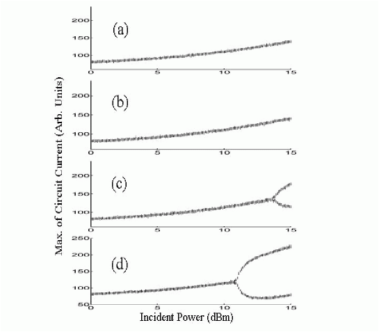
The DC bias nonlinearity can have a significant effect on the bifurcation diagram of the driven RLD circuit.[24, 25] As a DC bias is applied, the storage time and differential capacitance change, and the relationship between f0, 1/, and the driving frequency f will change. As discussed above, this can influence whether or not chaos is observed in the circuit. Here we present an example of the complex dynamics that can result. Figure 8 shows a case where the driving frequency f is larger than 1/ and about two to three times the RLD circuit resonant frequency f0 at zero DC bias. In this bifurcation diagram we see only period-1 behavior for driving signal power up to +15 dBm for both zero and positive DC bias. However, for negative bias, we see period doubling set in at about +14 dBm for a -0.4 V bias and about +11 dBm for a -0.6 V bias. The prevailing NLC models cannot explain this observation because a negative bias moves the diode away from the nonlinear part of the C(V) curve. In this case we believe that the increase in 1/ and increase in f0 due to VDC create a situation where f f0 1/, and the circuit displays period doubling at frequencies where ordinarily it only shows linear response.
It should be noted that period doubling and chaos can be observed in models of the driven RLD circuit even in the apparent absence of reverse recovery.[3, 10, 26] However, it is not clear to what extent these models may have discharge-time effects that mimic the behavior of reverse recovery in diodes.
V Discussion
To make further comparisons between the nonlinear capacitor (NLC) and reverse-recovery time models of RLD dynamics, we wish to further consider the simplified PLC model of the NLC. The PLC model contains the essential physics of all NLC models, and is very easy to implement and understand. Figure 2(a) (dashed line) shows that the PLC model of the diode (Fig. 3(b), inset) clearly shows an effective delay in ”turning off” after a large forward current has been applied to the device. This delay is a combination of two RC time constants. The first, or ”storage” part of the response is associated with the RC discharge of the PLC during its high-capacitance phase. As the voltage drop on the PLC decreases, it reaches the point (V = E0) where the capacitance switches to its smaller value, resulting in a much more rapid discharge, resembling the transition phase of reverse recovery. The simulation in Fig. 2(a) (dashed line) for the PLC qualitatively resembles the data on the 1N4007 diode. (Note that this simulation is not intended to fit the precise behavior of the 1N4007 diode, but to simply reproduce the essential behavior.)
The history dependence of the discharge time for the PLC model is illustrated in Fig. 3(b) (all simulations of the PLC model are done in SPICE). The discharge time is clearly enhanced after the second pulse of a two pulse sequence, compared to just a single pulse. This result is similar to that in Ref. [18] and Fig. 3(a) on real diodes. There is also strong frequency dependence to the discharge time of the PLC model, as illustrated in Fig. 5(b). The PLC capacitor model alone shows a discharge time that varies as 1/f. When a linear resistor is added in parallel with the PLC, the discharge time drops more slowly with frequency (PLC +R in Fig. 5(b)). Finally, when a nonlinear resistor (NLR) is added in parallel to the PLC, using the ideal diode IV curve of Linsay [1], the discharge time shows behavior remarkably similar to the reverse recovery time of a real diode.
In summary, the discharge behavior of the simple PLC model (when implemented in the circuits of interest) is remarkably similar to the reverse recovery behavior of real diodes. We find that SPICE simulations of other more sophisticated NLC models give very similar results. We conclude that all NLC models will show a reverse-recovery-like effect. It appears that the discharge of the NLC/PLC model is essentially the same as the diffusion of charge carriers out of the p-n junction. Hence this important ingredient of nonlinear physics is common to the two major models of nonlinear dynamics of the driven nonlinear resonator. However, our results demonstrate that all of these models lack key additional nonlinear properties of the reverse-recovery time.
VI Conclusions
We maintain that reverse recovery is a key effect producing chaos in the sinusoidally driven RLD circuit. All nonlinear capacitor models of this circuit have a behavior that mimics reverse recovery. Both the reverse-recovery and nonlinear capacitor models have memory built into them through a charge storage mechanism. The details of these models are different, but the results for circuit dynamics are basically the same. We find that it is not useful to make the distinction that either the nonlinear capacitance or the reverse recovery on minority carriers is the cause of chaos, because they can have similar effects on the circuit dynamics. Finally, the reverse recovery time in real diodes is a strongly nonlinear function of forward bias current, driving frequency and DC bias. A detailed understanding of chaos in the RLD circuit must include the reverse recovery effect and all of its nonlinearities.
VII Acknowledgements
This work was supported by STIC through the STEP Program, and by the Department of Defense MURI Program under AFSOR Grant F496 200 110 374. R. M. de Moraes was also supported by CAPES-Brazil. We acknowledge helpful discussions with Tom Carroll, and early work on the circuit was done by Sang-Ho Bok.
REFERENCES
- [1] P. S. Linsay, Phys. Rev. Lett. , 1349-1352 (1981).
- [2] J. Testa, J. Perez, and C. Jeffries, Phys. Rev. Lett. , 714-717 (1982).
- [3] E. R. Hunt, Phys. Rev. Lett. , 1054 (1982); reply by J. Testa, J. Perez, C. Jeffries, Phys. Rev. Lett. , 1055 (1982).
- [4] R. W. Rollins and E. R. Hunt, Phys. Rev. Lett. , 1295-1298 (1982).
- [5] D. S. Brorson, D. Dewey, P. S. Linsay, Phys. Rev. A , 1201-1203 (1983).
- [6] T. Matsumoto, L.O. Chua, S. Tanaka, Phys. Rev. A , 1155-1157 (1984); S. Tanaka, T. Matsumoto, L. O. Chua, Physica D , 317-344 (1987).
- [7] R. Van Buskirk and C. Jeffries, Phys. Rev. A , 3332-3357 (1985).
- [8] Z. Su, R. W. Rollins, and E. R. Hunt, Phys. Rev. A , 2698-2705 (1989).
- [9] J. Millman and C. C. Halkias, Integrated Electronics: Analog and Digital Circuits, McGraw-Hill, New York, 1972.
- [10] T. L. Carroll, and L. M. Pecora, Phys. Rev. E , 046219-1:046219-8 (2002).
- [11] A. Azzouz, R. Duhr, and M. Hasler, IEEE Trans. Circuits Sys. , 913-914 (1983).
- [12] Renato Mariz de Moraes and Steven M. Anlage, ”Effects of UHF Stimulus and Negative Feedback on Nonlinear Circuits,” submitted to IEEE Trans. Circuits Systems I. http://arXiv.org/nlin.CD/0208039.
- [13] T. Klinker, W. Meyer-Ilse, W. Lauterborn, Phys. Lett. A , 371-375 (1984).
- [14] J. M. Perez, Phys. Rev. A , 2513-2516 (1985).
- [15] V. V. Astakhov, B. P. Bezruchko, Ye. P. Seleznev, Sov. J. Commun. Tech. & Elec. , 83-90 (1988).
- [16] J. H. Baxter, M. F. Bocko, D. H. Douglass, Phys. Rev. A , 619-625 (1990).
- [17] S. Tanaka, S. Higuchi, and T. Matsumoto, Phys. Rev. E , 6014-6028 (1996).
- [18] E. R. Hunt and R. W. Rollins, Phys. Rev. A , 1000-1002 (1984).
- [19] A. Azzouz, R. Duhr, and M. Hasler, IEEE Trans. Circuits Sys. , 587-588 (1984).
- [20] B. P. Bezruchko and E. P. Seleznev, Tech. Phys. Lett. , 800-801 (1994).
- [21] Carroll and Pecora[10] also noted that a more complicated nonlinear capacitor model shows a reverse-recovery-like effect, but did not investigate its history dependence.
- [22] G. W. Neudeck, The PN Junction Diode, Addison-Wesley, Reading, MA, 1989.
- [23] D. J. Roulston, Bipolar Semiconductor Devices, McGraw-Hill, New York, 1990, p. 97.
- [24] A. S. Maksimov and N. A. Maksimov, Sov. Phys. Tech. Phys. , 939-940 (1989).
- [25] C. M. Kim, G. S. Yim, Y. S. Kim, J. M. Kim, H. W. Lee, Phys. Rev. E , 2573-2577 (1997).
- [26] C.-M. Kim, C.-H Cho, C-S. Lee, J.-H. Yim, J. Kim, and Y. Kim, Phys. Rev. A , 1645-1648 (1988).
| Diode | (ns) | Cj (pF) | Results with | Results with | Results with |
|---|---|---|---|---|---|
| f0 1/ | f0 10/ | f0 100/ | |||
| 1N5400 | 7000 | 81 | Period doubling and | Period doubling and | No period doubling |
| chaos for | chaos for | or chaos | |||
| f/f0 0.11 - 1.64 | f/f0 0.16 - 1.76 | ||||
| 1N4007 | 700 | 19 | Period doubling and | Period doubling and | No period doubling |
| chaos for | chaos for | or chaos | |||
| f/f0 0.13 - 2.0 | f/f0 0.23 - 1.3 | ||||
| 1N5475B | 160 | 82 | Period doubling and | No period doubling | No period doubling |
| chaos for | or chaos | or chaos | |||
| f/f0 0.66 - 2.2 | |||||
| NTE610 | 45 | 16 | Period doubling and | Period doubling | No period doubling |
| chaos for | for | or chaos | |||
| f/f0 0.14 - 3.84 | f/f0 1.17 - 3.25 |