A Dedicated Computer for Ising-like Spin Glass Models
Abstract
We present a parallel machine, based on programmable devices, dedicated to simulate spin glass models with variables and short range interaction. A working prototype is described for two lattices containing spins each with an update time of 50 ns per spin. The final version of the three dimensional parallel machine is discussed with spin update time up to 312 ps.
keywords:
Ising model, spin-glass, +/-J, 2d, dedicated machine, programmable logic.PACS:
07.05.Bx, 02.70.Lq, 05.50.+q., and
DFTUZ/96/19 hep-lat/9611014
1 Introduction
Lattice Monte Carlo simulations are an important tool for the physicists working in Quantum Field Theory and Statistical Mechanics. These kind of simulations require large amounts of computational power and the processing can be often parallelized. Therefore, various groups have developed their own parallel machines for these simulations [1] [2] [3] [4].
The appearance in the market of very large programmable components (PLD) [5] makes it possible to design dedicated machines with low cost and high performance. The performance of these machines is increased due to the fact that they can run more than a single model: the lattice size or the action of the physical model can be easily changed by reprogramming the PLD.
At present, spin glass models [6] are an area of Statistical Mechanics in progress. They are easily implementable on this kind of machines because they require very simple calculations. These models are related to neural networks, spin models, some High superconductivity models, etc.
In this paper we describe a PLD-based machine, dedicated to three dimensional spin glass models with variables belonging to and couplings to first and second neighbours.
From the physical point of view, a standard way of studying the model is by using several independent lattices, called replica [6]. For this reason we use parallel processing in our machine, running independent lattices, in a similar manner to the multi-spin code used in conventional computers.
An essential tool for the analysis of the results is Finite Size Scaling [7] which requires the use of different volumes. Our machine is capable of working with different sizes of lattices by reprogramming a few components. Also, it is possible to run on a single large volume considering the n spins living on the same lattice. This option is more efficient if the thermalization time is very large.
The algorithm chosen for the simulation is the demon algorithm proposed by Creutz [8]. It has been chosen as a starting point because of its simplicity since it does not require a random number generator for the update.
At present we have built a bidimensional prototype with first neighbours couplings. We use this prototype in this paper to explain how the machine works and the generalization to the case is discussed later.
2 The Physical Model
The model we want to simulate is the 3-d Ising-like spin glass model with first and second neighbour couplings (see [6] for a detailed description of the model). The action of this model is given by the expression
| (1) |
where the value of the spins can be only or . The same for the couplings (multiplied by a constant). While the spins are variables, the distribution of couplings is fixed. For a fixed set of the partition function is
| (2) |
To calculate (2) we must sum over possible configurations, where is the volume of the lattice, which is a very large number for any computer. The standard way to compute the partition function is to run an algorithm that selects only a representative set of configurations. There are different algorithms to do that. See for instance the Sokal chapter in [9]. For pure spin systems (all equal to ) some cluster algorithms are very efficient, but for a general spin glass model, only local algorithms achieve good efficiency. Typically we must run the algorithm and generate millions of different representative configurations in order to obtain accurate results.
The prototype simulates a bidimensional model with nearest neighbour couplings only:
| (3) |
The algorithm we use is a microcanonical one. It keeps constant the sum of the energy of the lattice and a demon. In order to generate the representative set of samples, we start from a spin configuration with an action and a demon energy equal to zero.
Now we use the algorithm to change the spins to generate new configurations (one for every updates). The update of a spin is as follows: if the flip lowers the spin energy, the demon takes that energy and the flip is accepted. On the other hand, if the flip grows the spin energy, the change is only made if the demon has that energy to give to the spin.
At this level, the value is missing and can be obtained in two ways. We can compute the mean energy of the demon over all the sample, , and then we obtain the value as
| (4) |
Also if the probability distribution of the demon energy is computed, , the behaviour of this function is given by the expression
| (5) |
A fit to this function provides us the value.
For simplicity, in case of the prototype machine we use periodic boundary conditions in one direction and helicoidal in the other (see paragraph 4.1). The biggest lattice we can simulate has a size of 312 by 312 spins. We process two independent lattices as an example of how the parallelism can be implemented. For spin glass systems these independent configurations represent two replicas. By reprogramming some components we can simulate either two smaller lattices or a single larger lattice (, or similar geometries).
3 Operation and General Structure of the Machine
We now describe how the machine performs the simulation.
We assign numbers to the the sites of a lattice from 0 to , where is the volume of the lattice. A sequential update is made by selecting the spins in the chosen order (see paragraph 4.1).
To update the spin, its four nearest neighbours have to be supplied to the updating engine, too. Then both the local energy and the local energy with the flipped spin are computed. The energy balance of the flip is consequently computed to decide whether the flip is accepted:
-
•
If then the flip of the spin is accepted and the demon energy is increased in .
-
•
If , but , the flip is accepted and the demon energy decreases in .
-
•
Otherwise the flip is rejected and the spin does not change its value.
These steps are repeated for each spin of the lattice. In order to obtain an updated spin every clock cycle we have designed a pipeline structure that performs the latter algorithm step by step.
For all lattices processed in parallel, the spins to be updated as well as their neighbours can be stored in memory in such a way that each bit of the memory word belongs to a different lattice. The calculation of the energy balance is independent for each lattice, so this part of the hardware must be repeated for any of the lattices processed in parallel.
Now, we give a brief survey of the structure of the spin machine that performs the previous algorithm. The machine (let us call it SUE, for Spin Updating Engine) is connected to a Host Computer (HC). SUE performs the update of the configurations and the measurement of some local operators, such as the energies and magnetizations. The rest of measurements are made by HC. Anytime a complete configuration has been updated, HC can read the values of the demons from SUE and periodically, after a certain number of iterations, SUE is stopped and the configuration is downloaded to HC.
Fig. 1 shows a simple diagram of the machine which consists of a motherboard equipped with slots for processing modules (the figure is for ), PCI interface and control logic. The motherboard provides power supply distribution, data interconnection, and allows HC to control the processing modules via the PCI interface which is indispensable to perform data transfers from/to the modules. Every processing module contains the hardware to store and update a set of lattices in parallel. Note that there are two degrees of parallelism: inside the processing module and between the modules.
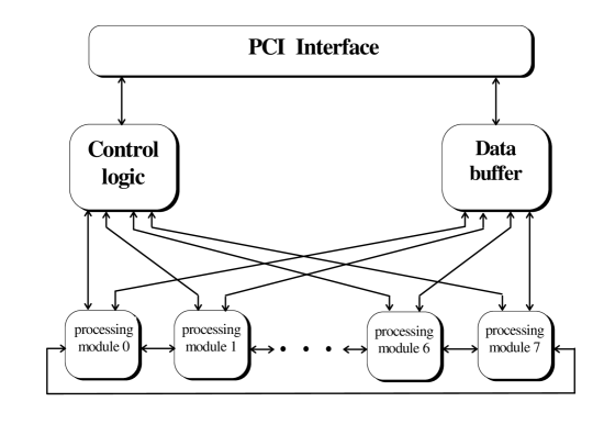
By processing 8 spins in parallel on 8 modules (64 spins in total) within one clock cycle (clock period of 50 MHz), we obtain an update speed of 312 ps/spin, a performance more than one order better than that of the supercomputers available today.
4 The Prototype.
The prototype we have built shows how a processing module works, its inner architecture and the placement of the algorithm of the simulation in electronic devices. It also contains the input/output logic which can be handled from a host equipped with a data acquisition card.
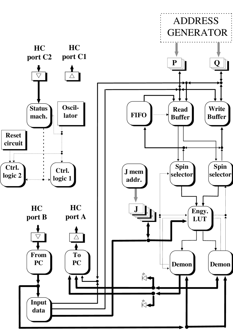
We have used the PLD’s Altera EPM7032-10 [5] to build the logic and the static RAM’s (SRAM) KM62256-8. The speed grade of the SRAM limits the maximum frequency of operation of the machine to 10 MHz. SUE performs two updates at every clock cycle, one for each lattice, so the theoretical performance is that a spin is updated in 50 ns. We have designed a pipeline structure (discussed later), in order to obtain an updated spin by cycle. Fig. 2 shows the block diagram of the board: every square is an Altera programmable chip, the overlapped rectangular boxes are memory chips and the daughter board is an address generator (see paragraph 4.3) that contains seven Altera chips.
The logic can be divided into five groups: addressing (daughter board), spin selection, update, control and I/O logic.
The addressing logic prepares addresses for the fetched and stored (updated) spins. The core of the addressing logic is a set of multiplexed counters which provide the address for the spin memory.
The spin selection logic contains a subset of the lattice. It selects the spin to be updated and its neighbours and sends them to the update logic. Each clock cycle it receives an updated spin from the update logic.
The update logic takes the selected spins, the couplings between them, and the demon energy from an 8-bit register and carries out the update algorithm, sending the new spin to the spin select logic.
The control logic is a state machine that handles the set of internal signals during the simulation and during the data transfer periods, and in addition to the input/output logic it allows the reading and writing of the memory chips and the demon registers, starting and stopping the machine.
The following subsections explain in detail step by step the function of the different devices of the prototype.
4.1 Spin Storage in Memory
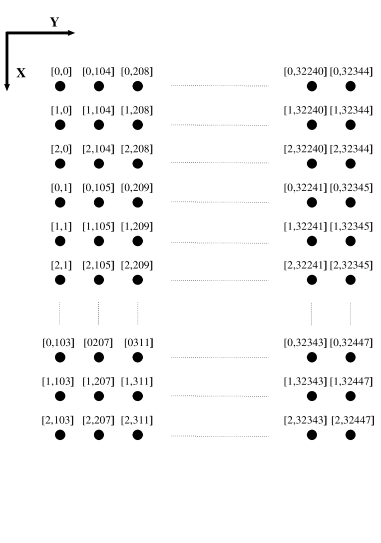
We want to store a square lattice of side L, with spin positions labelled by . Let L be a multiple of 3. That is because we store the whole lattice into three memory chips of 32k words. We use the least significant bit of the word to store the first lattice and the next one to store the second one. Then each address contains three spins of a lattice, one from each memory chip.
The storage procedure is as follows: every column in the lattice is divided into blocks of three spins each (hereafter, the block will be the basic unit for labelling the lattice); the first spin of any block is stored in chip 0, the second spin in chip 1 and the last spin in chip 2, but the important fact is that the generated addresses are the same for all the chips and depend only on the block label. We number the blocks vertically in the XY plane, beginning from 0 on the top left corner, and then down in the X direction. The last block in the first column is the . We continue with the second column and so on. The last block of the lattice has the number . The individual spins are numbered in the same way, from 0 to , and this is the chosen order for carrying out the sequential update.
We present here a nomenclature which will help to clarify the idea. Let us also tag the spins according to the position they occupy in memory, in the way . Notice that here we use and for the position in the physical lattice we use . There is a relationship between these two nomenclatures:
| (6) |
As said above, the address where a spin is stored is actually the number of the block in which this spin can be found. Fig. 3 shows the distribution of spins in memory for the case of a lattice with spins.
In order to write the new spin values during the same read cycle and for doing this in a completely automatic manner, the solution is to duplicate the memory. Then we have two banks of memory (three chips each) which we call BankP and BankQ. We use the following update procedure. We want to update a column of spins which are read from a bank (i.e. BankP) with the neighbour columns. The updated spins are written into the second bank (BankQ). When the column update is finished, the role of the banks is changed for the next column: we read the lattice with the recently updated spins from BankQ and the newly updated spins are stored into BankP. The neighbour columns are written too (see paragraph 4.2), and due to the fact that an updated column is a neighbour column for the next one, the two banks finally contain the updated configuration.
The Read Buffer device (Fig. 2) has access to the spin memory data lines. The Write Buffer chip generates a parity bit which is stored together with the updated spins during the write cycles and it is checked during the read accesses. The update process takes 8 clock cycles from the instant the spin is read until it is updated, so a small buffer FIFO is required in order to bridge over the change of the role of the memory banks. This component stores the first updated spins of the column being processed.
4.2 Spin Selection Logic
The read blocks corresponding to a lattice are written in a sequential way in the Spin Selector device which contains registers (3-bit wide) to store a subset of the lattice. Table 1 shows these registers:
At every moment we have a copy of a certain region of the lattice ( spins) in these registers. Only spins in registers B and E will be updated, moving from 0B through 2E. In order to update a spin situated in a position of these registers, its neighbours must be correctly placed in the rest of the registers. This component contains a state machine that performs repeatedly 6-step loops with the following structure:
-
•
Step 0:
-
–
Register A is sent to the Write Buffer and replaced by the following block.
-
–
Spin 0E is sent to the update logic.
-
–
Spin 1B updated is received.
-
–
-
•
Step 1:
-
–
Register B (the updated spins) is sent to the Write Buffer and replaced by the following block.
-
–
Spin 1E is sent to the update logic.
-
–
Spin 2B updated is received and sent to the Write Buffer with the other two spins (already updated) of its block.
-
–
-
•
Step 2:
-
–
Register C is sent to the Write Buffer and replaced by the following block.
-
–
Spin 2E is sent to the update logic.
-
–
Spin 0E updated is received.
-
–
-
•
Step 3:
-
–
Register D is sent to the Write Buffer and replaced by the following block.
-
–
Spin 0A is sent to the update logic.
-
–
Spin 1E updated is received.
-
–
-
•
Step 4:
-
–
Register E (the updated spins) is sent to the Write Buffer and replaced by the following block.
-
–
Spin 1A is sent to the update logic.
-
–
Spin 2E updated is received and sent to the Write Buffer with the other two spins (already updated) of its block.
-
–
-
•
Step 5:
-
–
Register F is sent to the Write Buffer and replaced by the following block.
-
–
Spin 2A is sent to the update logic.
-
–
Spin 0A updated is received.
-
–
The order in which blocks are read from memory and loaded into the corresponding Altera register is given in the table 2, from left to right and top to bottom.
| C0 | C1 | C2 |
|---|---|---|
As shown in table 2, the three columns contain memory locations with the spin to be updated (column C1) and its neighbour spins. All three columns (one line) has to be fetched before the update procedure of the spins can be started. In this way, all memory locations are read and updated. The blocks in column C0 feed the A and D registers, in column C1 the B and E registers, and in column C2 the C and F registers. The spins to be updated are always loaded into either the B or E registers. Remark that the previously updated column feeds the A and D registers.
4.3 Addressing Logic.
As can be seen from table 2, it is very simple to generate the sequence of addresses to select the blocks which are read from memory, and the order in which the blocks are written into memory. The order is the same, but shifted a few cycles. For this reason, it is adequate to have two sets of three counters (C0, C1, C2): one for reading and the other for writing. They correspond to the columns in table 2, so C0 begins to count from 0, C1 begins from 104 and C2 begins from 208, and they pass through all the values from 0 to .
These counters and their multiplexes are programmed in a Daughter Board which is a plug-in module of SUE.
4.4 Update Logic.
The update logic takes the spin to be updated and their neighbours in order to calculate the amount of energy that the flip requires. One of the neighbour spins arrives directly from the update logic. The four couplings that link the spins are read from a memory bank (J). This memory is addressed by the J Mem. Addr. device. This bank is deep by bits wide. As only four bits are used for one lattice, two sets of couplings for two different lattices can be stored in a single memory word. We have also incorporated a parity bit which is checked by the Energy Look Up Table (LUT) device. The update procedure is carried out in two clock cycles. During the first cycle the spins and their relative couplings are fed into the Look Up Table whose output is the energy balance of the update. Along the second cycle this value is added to the demon energy in the device called Demon and the sign of the sum is checked. If this sign is greater than or equal to zero, the flip is accepted and the demon changes its value. If the sign is lower than zero, the spin and the demon do not change. The updated spin is fed back to both the LUT and spin selection logic.
4.5 Status Machine.
The way in which the SUE works is programmed as a big status machine in the Status Machine component. This chip receives the instructions released by HC and together with the Control Logic chips it generates a set of signals required to control the memories, buses, etc.
4.6 Input/Output Logic.
HC is connected to SUE via a data acquisition board based on 8255A-like controller with interrupt request (IRQ) capabilities. We use two 8-bit ports (A,B) and two 4-bit ports (C1,C2). A and C1 ports are output for SUE while B and C2 are input ports. The 8-bit ports are used for data transmissions, and C2 is used to give instructions to SUE. The signals in C1 are the IRQ, the reset signal and the two parity errors checked. From PC, To PC and Input Data components allow HC to access to the different memory banks and registers of SUE.
The following set of instructions is available through the port C2:
-
•
Reset.
-
•
Read/write demon energy for the first lattice.
-
•
Read/write demon energy for the second lattice.
-
•
Read/write a spin block (the two lattices at the same time).
-
•
Write a coupling word.
-
•
Start simulation.
The normal operation of SUE is as follows:
-
•
Store couplings in J-memory.
-
•
Store spins in spin memory.
-
•
Write the initial demons’ energies.
-
•
Start simulation.
When the start instruction is executed, SUE reads a number from the data acquisition board and it begins to generate updates of the initial configuration. Every time an update of the configuration is completed, SUE generates an IRQ to HC and the demon registers can be read by HC. When the updates are performed, the SUE stops and HC can download the spin configurations. In order to restart the simulation it is not necessary to rewrite the configurations, but to execute again a start instruction. Data transmission speed through the ISA DAQ card is 2 kBytes/s, so storing a configuration of spins takes .
5 Design Considerations and Final Product
As it was formerly said, for the prototype version we have used the PLD’s Altera EPM-7032-10. The logic has been designed with registered logic and short propagation delay times, so the highest frequency of operation is fixed by the memory access time to 10MHz. In these conditions, we obtain two updated spins in 100 ns. Nevertheless, the reliability of the double side printed circuit board allows us to work at 5MHz only. Consequently, the real update speed of this machine is 1 updated spin in 100 ns.
We can compare SUE performance versus a general purpose computer: We have written an optimized program that runs the same model, simulating 8 lattices at the same time. With this degree of parallelism, a 120 MHz Pentium PC takes 1000 ns in order to update 1 spin.
6 Physical Results
In order to check the SUE performance and their reliability we have run a simulation on the critical point of the Ising model. The exact (analytical) solution of this model is known and so obtaining the correct value is a very good test for the SUE’s global functionality. We start with a configuration as close as possible to the critical energy . The obtained value from the simulation using (4) and (5) has to be .
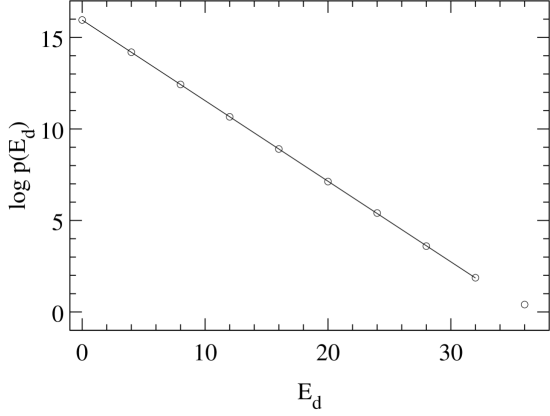
Due to the fact that the first configuration is very far from the equilibrium (it is not in the representative sample), we must thermalize it first. We do that by running iterations. Then we run iterations to measure. After every iteration (update of spins) SUE outputs the demon energy to HC. Every 1024 iterations the full configuration is downloaded to HC and checked in order to control that the global energy has not changed.
From (4) we obtain to be compared with the exact value . The small difference is due to the Finite Size Effects because the exact is only obtained in the limit . In this case, the shift in [10] is
| (7) |
which makes results compatible.
7 The Generalization
The three-dimensional machine should be based on the same philosophy as the currently working prototype for . The Spin Selector has to be extended in order to store a greater region of the lattice. A simple extension is described here.
For the three-dimensional lattice we have to use blocks of 9 spins each, keeping the same numbering system of blocks as before, plane by plane. The first plane has blocks from 0 to . The next plane has its blocks numbered from to . The last plane begins in the block and ends in the block.
Fig. 5 shows the extension of the Spin Selector logic. We use 18 registers, 8 bits each: the central registers (E,N) contain the spins to be updated and the rest of the registers store the neighbours: The D (M), E (N) and F (O) registers contain the neighbours in the same plane; The A (J), B (K) and C (L) registers store the neighbours in the plane below, and the G (P),H (Q) and I (R) registers store the neighbours corresponding to the plane above. The neighbours of two spins have been depicted in the figure, besides the localization of the 9-tuples in the lattices. The spins to be updated are selected along the axis. Remark the boundary conditions between the two sets of 9-tuples.
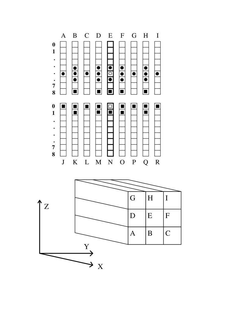
The addressing logic has to provide addresses in such a way that the registers are fed in alphabetical order. For instance, when the spin is sent to the update logic, the block is read from memory. This component will perform a loop of 18 different states, like the 6-state loop for the bidimensional case.
The addressing logic keeps the structure of multiplexed counters. The boundary conditions are periodical in one direction and helicoidal in the other two directions.
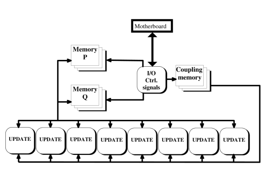
For the construction of this board the high capacity Altera PLDs’ (CPLD) and fast Static RAMs (with access time) has to be used. In this way, each of the two memory banks P and Q will consist of from nine SRAM components. The 8-bit word is used in order to run 8 independent lattices and 9 memory components to build the 9-bit blocks. The largest symmetric lattice that can be stored with multiple of 9 is spins. The I/O and control logic will be placed in a single PLD and the Spin Selector and Update Logic into another PLD. Modules bearing the latter PLDs allow us further segmentation of the lattices and to speed up the spin update time (see fig. 6).
As the memory access time determines the maximum clock frequency (50 MHz), this board can make an update in . A motherboard with 8 plug-in modules can reach an update time of 312 ps per spin.
We also want to include into the latter PLD’s a random number generator in order to run a canonical simulation. The random number generation is a time consuming task in a general purpose machine, making slow the simulation. In a dedicated machine this generation can be carried out without time loss, raising its performance with respect to conventional computers.
We wish to thank J. Carmona, D. Iñiguez, J. J. Ruiz-Lorenzo, G. Parisi and E. Marinari for useful discussions. Partially supported by CICyT AEN93-0604-C01 and AEN94-0218. CLU is a DGA Fellow.
References
- [1] The APE Collaboration, Comp.Phys.Com. 57 (1989) 285.
- [2] N. H. Christ and A. E. Terrano, IEEE Trans.Comput. 33 (1984) 344.
- [3] The RTN Collaboration, Procc. of CHEP 92 CERN 92-07.
- [4] A. Hoogland, J. Spaa, B. Selman and A. Compagner, J.Comp.Phys. 51 (1983) 250.
- [5] Altera Corporation, Altera Data Book 1995.
- [6] M. Mezard, G. Parisi and M. A. Virasoro, Spin Glass Theory and Beyond. World Scientific 1997.
- [7] M. E. Fischer and A. Nihat Baker, Phys.Rev. B26 (1982) 2507.
- [8] M. Creutz, Microcanonical Monte Carlo Simulation. Phys.Rev.Lett. 50-19 (1993).
- [9] M. Creutz, Quantum Fields on the Computer. World Scientific 1992.
- [10] A. E. Ferdinand and M. E. Fisher, Phys.Rev. 185 (1969) 832;