Status of the CP-PACS Project ††thanks: Presented at Lattice 96, St. Louis, USA.
Abstract
The CP-PACS computer with a peak speed of 300 Gflops was completed in March 1996 and has started to operate. We describe the final specification and the hardware implementation of the CP-PACS computer, and its performance for QCD codes. A plan of the grade-up of the computer scheduled for fall of 1996 is also given.
1 CP-PACS project
The CP-PACS project[1] is a five-year project which formally started in 1992. The project currently consists of 33 members in physics and computer science as listed in Ref. [2]. We selected Hitachi Ltd. as the industrial parter through a formal bidding process soon after the start of the project, and we have been working in a close collaboration for the hardware and software development of the CP-PACS computer. The fundamental design of the computer was laid down in 1992, its details worked out in 1993, and the logical design and the physical packaging design was completed in 1994. Chip fabrication and assembling of parts started in early 1995, and the CP-PACS computer with a peak speed of 300 Gflops was completed in March 1996.
| peak speed | 300Gflops(64 bit data) |
|---|---|
| main memory | 64GB |
| parallel architecture | MIMD with |
| distributed memory | |
| number of nodes | 1024 |
| node processor | HP PA-RISC1.1+PVP-SW |
| #FP registers | 128 |
| clock cycle | 150MHz |
| 1st level cache | 16KB(I)+16KB(D) |
| 2nd level cache | 512KB(I)+512KB(D) |
| network | 3-d hyper-crossbar |
| node array | |
| through-put | 300MB/sec |
| latency | sec |
| distributed disks | 3.5” RAID-5 disk |
| total capacity | 529GB |
| software | |
| OS | UNIX micro kernel |
| language | FORTRAN, C, assembler |
| front end | main frame |
| connected by HIPPI | |
| ∗ including nodes for I/O | |
2 Hardware implementation
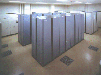

A picture of CP-PACS computer is shown in Fig. 1. The size of the computer is roughly 2m4m3m in height, width and depth. The floor-plan is depicted in Fig. 2. For the major architectural characteristics of the computer I refer to Ref. [1].
The final specification of the CP-PACS computer is summarized in Table 1. The size of the second-level cache has been doubled since last year. The number for latency of data transfer represents the measured value in the remote DMA mode, which is the fastest mode for data transfer, including software and hardware overheads and averaged over transfer through , and crossbar switches.
Figure 3 shows the floor plan of the CPU chip which is fabricated by 0.3 micron CMOS semiconductor technology, with the size being 1.57cm1.57cm. The PVP-SW feature, which enables vector calculations very effectively within the RISC architecture of CPU, is implemented with 128 floating-point registers in the green part at the lower right corner of Fig. 3.
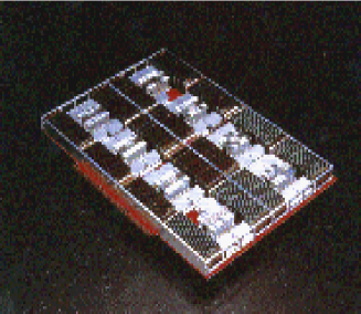
A silicon multichip module is depicted in Fig. 4 where the chip located at the center is the CPU chip. The adjacent two chips are the network interface adapter (NIA) and the storage controller (SC) which are fabricated by 0.5 micron gate-array technique. Twelve chips surrounding them are off-chip second-level cache made of SRAM. The size of the module is about 5.7 cm 7.2 cm.
One board which consists of 8 nodes is shown in Fig. 5. The center of the white part of each unit corresponds to the multichip module shown in Fig. 4, now with fins for air-cooling. The black part is the main memory with 4 Mbit DRAM. The other three white chips on each unit are main-memory address/data controllers. In addition each board has two chips for crossbar switches in the direction and one chip for clock distributer. The size of one board is 45.6 cm 62.5 cm. Sixteen boards are installed in a crate and two crates are installed in a cabinet represented by a square with symbol P in Fig. 2.
The crossbar switches in the direction are mounted on each board connecting 8 nodes, as explained above, those in the direction placed on a back-plane located in four cabinets (symbol P in Fig. 2) and those in the direction mounted on a board which is housed in one cabinet (symbol Z in Fig. 2).
In the two cabinets with symbol IOU, adaptors for I/O of data to the distributed disks are installed. Raid-5 disks which are connected by SCSI-2 bus through the adaptors are set in cabinets installed a few meters apart.
3 Performance
We write codes for lattice QCD with Fortran 90 which includes libraries for data communication. A Fortran compiler incorporating the PVP-SW feature has been newly developed, which produces efficient object codes. The performance of the object code is typically 90 – 150 Mflops per node, depending on the structure of the do-loop. The through-put of the data transfer between nodes with Fortran libraries, in the case of data of 576 Kbytes as an example, is 250 Mbytes/sec, which is to be compared with the peak through-put of 300 Mbytes/sec.
The update time per link with a pseudo-heat bath method for one processor is 55.3 sec, which corresponds to 103 Mflops/PU. The performance for the Wilson quark matrix multiplication for the red-black algorithm is 96 Mflops/PU with the present code. On the other hand, we have a hand-optimized assembler code for the Wilson quark matrix multiplication with which the performance reaches 195 Mflops/PU, which is 65 % of the peak speed. We are now modifying this assembler code for the red-black algorithm. For MR red/black solver, the performance of the calculation part is 122 Mflops/PU, which reduces to 93 Mflops/PU when the data communication is included. The percentage of communication is about 20 % of the total time. In the case of the CG solver for KS fermion, the performance is 128 Mflops for the case when the length of the inner most loop is 128.
After checking the fundamental performance, we have performed a test of the computer as a whole with a quenched QCD spectrum calculation with the Wilson quark action on a lattice at for three hopping parameters (, 0.5, and 0.4), for two of which there exist already previous mass spectrum calculations. Results for the effective masses of hadrons for the smaller two hopping parameters are in good agreement with the previous results. This makes us confident that the machine is working properly and that our codes are correct.

4 Grade-Up of the CP-PACS computer
We plan to grade-up the CP-PACS to a peak speed of 600 Gflops and a memory size of 128 Gbytes, increasing the number of nodes from 1024 to 2048 in the coming fall. The total funding approved including that for the grade-up is 2.2 billion yen (about 22 million US dollars). Until the grade-up we plan to run a quenched spectroscopy calculation with Wilson quarks at four values of in the range of to 0.75 on lattices with a spatial size 3.0 fm.
This work is supported by the Grant-in-Aid of Ministry of Education, Science and Culture (No.07NP0401).
References
- [1] Y. Iwasaki, Nucl. Phy. B(Pro. Suppl)34(1994) 78, A. Ukawa, ibid. 42(1995)194.
- [2] The present members of the CP-PACS project are: S. Aoki, T. Boku, M. Fukugita, S. Gunji, T. Hoshino, S. Ichii, M. Imada, S. Ishizuka, Y. Iwasaki, K. Kanaya, H. Kawai, T. Kawai, M. Miyama, S. Miyashita, M. Mori, Y. Nakamoto, H. Nakamura, T. Nakamura, I. Nakata, K. Nakazawa, K. Nemoto, M. Okawa, A. Oshiyama, Y. Oyanagi, S. Sakai, T. Shirakawa, A. Ukawa, M. Umemura, K. Wada, Y. Watase, Y. Yamashita, M. Yasunaga, and T. Yoshie.