The status of US Teraflops-scale projects
Abstract
The current status of United States projects pursuing Teraflops-scale computing resources for lattice field theory is discussed. Two projects are in existence at this time: the Multidisciplinary Teraflops Project, incorporating the physicists of the QCD Teraflops Collaboration, and a smaller project, centered at Columbia, involving the design and construction of a 0.8 Teraflops computer primarily for QCD.
1 INTRODUCTION
Along with new analytic approaches and algorithmic improvements, increasing computational power is an obvious avenue for progress in lattice field theory, particularly QCD. To achieve a significant increase in physical volume and a decrease in lattice spacing requires a large increase in computer power, precipitating a move to machines of the Teraflops scale. On such machines, calculations with dynamical fermions should have statistical errors and control of systematic errors from finite volume and non-zero lattice spacing comparable to the best quenched calculations of today.
There are currently three groups in the US doing calculations on dedicated, multi-Gigaflops scale computers built primarily for QCD; they are groups at Columbia, Fermilab and IBM. Currently, the IBM group has no plans for a next generation machine and the Fermilab group is investigating options for a machine to replace ACP-MAPS in the near future. Over the last few years, the members of the Columbia group were active participants in the QCD Teraflops Project, a US collaboration of many tens of physicists working to acquire a Teraflops-scale machine for QCD. This project involved a commercial partner, Thinking Machines Corporation, with a strategy centered on increasing the floating point power of a commercial machine for QCD.
In spring of 1993, a decision by Thinking Machines Corporation to discourage our use of the CM-5 platform for this enhanced machine and a decision by Texas Instruments (TI) not to participate in the floating point upgrade meant a serious delay in the development of this project. At that time, the Columbia group and a few collaborators began working to design and build a dedicated, inexpensive 0.8 Teraflops machine primarily for QCD. The Multidisciplinary Teraflops Project is the name generally given to the continued collaborative effort with Thinking Machines, with the QCD Teraflops Collaboration as a major part. We will focus on the status of these two projects
2 MULTIDISCIPLINARY TERAFLOPS PROJECT
The Multidisciplinary Teraflops Project has been seeking to develop enhanced floating point hardware to be mated with the network that Thinking Machines Corporation was planning for the successor to the CM-5. Another major goal has been the ability to make use of the existing Thinking Machines software tools. The QCD physicists working on this project will provide a major application for the resources provided by this relatively general purpose machine. The project also involves the Laboratory for Computer Science at MIT and Lincoln Laboratories.
The proposed machine is a 64 bit, MIMD computer with 512 floating point accelerators. Each accelerator is attached to a general communications network, producing a peak speed of 1.6 Teraflops with 250 Gbytes of memory for a cost of 25 million dollars. The recent bankruptcy of Thinking Machines Corporation has added a large measure of uncertainty to the project. At this time it is unclear whether Thinking Machines network technology will reappear in the marketplace, or whether another commercial network can be used, so we will not be able to detail the complete machine and instead will concentrate on the architecture of the the floating point accelerator, which has been under active development.
The accelerator consists of 16 Power PC 604 RISC processors, each connected to 32 Mbytes of local memory (either DRAM or synchronous DRAM) through a memory controller. In turn, each memory controller is attached to an industry standard, 64 bit wide, PCI bus with a bandwidth of 422 Megabytes/sec at 66 MHz. The Power PC processor supports multiple cache lines for efficient prefetching of data from the local memory, has 32 registers and a 32 kilobyte data cache. Each of the Power PC’s has a peak speed of 200 Mflops, giving the accelerator board a peak speed of 3.2 Gflops at an expected cost of $28,000.
The architecture has the memory controller for each processor capable of sending data to any other processor in the machine. The memory controller may only be able to transfer sequential blocks of data, ie. no block-strided transfer capability, which requires the occasional involvement of the Power PC to rearrange data before a transfer.
Simulations of this design have given estimates for the floating point performance of the application of the staggered Dirac operator. The simulator has been developed by members of the collaboration and uses their understanding of the cache structure of the Power PC to model its performance. Their results show sustained performance of about 1.15 Teraflops. The most heavily loaded bus is the one connecting the floating point accelerator to the 512-node network, and it is loaded at slightly below 50% of its capacity. These simulations do not include the global sums necessary in the staggered conjugate gradient.
There are currently efforts underway to check the performance of the accelerator on other applications, an important question given the multidisciplinary use expected.
3 THE COLUMBIA 0.8 TERAFLOPS COMPUTER
In the spring of 1993 a group led by physicists at Columbia began work on a computer capable of Teraflops scale computing for a few million dollars. We have pursued a strategy which makes as much use as possible of commercially available components arranged in an efficient form for QCD calculations. To this end, we have been working to design and construct a 0.8 Teraflops, 32 Gbyte, largely 32 bit precision, MIMD computer based on a four dimensional, array of 16,384 Digital Signal Processors (DSP’s) with 25 or 50 MHz bit-serial nearest-neighbor communication between processors[1]. The total price is 3 million dollars.
The members of the collaboration are
-
•
Columbia University:
Igor Arsenin, Dong Chen, Norman H. Christ, Chulwoo Jung, Adrian Kahler, Roy Luo, Robert D. Mawhinney, and Pavlos Vranas -
•
Columbia University Nevis Laboratory:
Alan Gara and John Parsons -
•
Fermilab:
Sten Hanson -
•
SCRI at Florida State University:
Robert Edwards and Tony Kennedy -
•
The Ohio State University:
Greg Kilcup -
•
Trinity College, Dublin:
Jim Sexton
The basic processing node of our machine (Figure 1) consists of a DSP, 1/2 Mword of memory (five chips) and a custom-made chip we call the node gate array (NGA). This seven chip processing node will fit on a double-sided printed circuit board of size about 1.8 inches by 2.7 inches, has an expected cost of $140 and will use 2–3 watts of power.

16,384 of these nodes gives a 0.8 Teraflops computer that uses around 50 kilowatts of power (the current Columbia 256-node computer uses 30 kilowatts) and contains roughly 110,000 chips (the 256-node computer has 80,000). For the DSP and DRAM chips we are using, the hardware failure rate is a few tens in a billion hours of use. Therefore, even with chips and hours in a year, we expect to have a few tens of failures per year, or roughly one every few weeks (after five years of running, the 256-node machine has one every few months). This low failure rate removes the need for fault-tolerant software and allows us to operate the machine only when there are no hardware failures.
3.1 Processor
To achieve Teraflops scale computing for a price of a few million dollars, processing power alone has to cost around one dollar for a Mflops. Our answer to this constraint has been to focus on Digital Signal Processors. Today, DSP’s are a commodity that appear in modems, CD players, etc. They are essentially microprocessors where the emphasis has been placed on arithmetic power (floating point power in our case) as opposed to, for example, context switching efficiency, which is necessary for a microprocessor handling a multitasking environment like a UNIX workstation.
We have chosen to use a Texas Instruments TMS320C31 DSP, a single precision, 50 Mflops DSP which is expected to be available in quantity for around $50. This chip uses about a watt of power and is available as a surface mount component. The CPU can perform two operations in a single 25MHz cycle; the instruction set includes parallel load-store operations as well as parallel multiply-add’s. In addition to 16 registers, there is a 2 kiloword memory inside the DSP which can supply two of the source operands for the parallel operations. The DSP also has an internal DMA, which can be used, for example, to load data into the on chip memory while the CPU is doing calculations. The DSP can also boot over a serial line, which precludes the need for 16,384 PROM’s.
3.2 Architecture
We have faced two main architectural challenges in turning a collection of processors into an efficient parallel machine. They are: to develop a simple, efficient, inexpensive communications network for QCD and to balance the speed of the DSP with the memory bandwidth available from DRAM. In this section, we will describe our solutions to these challenges.
3.2.1 Communication network
Given the large number of processors in our machine, a completely general communication network, such as a crossbar switch, is either prohibitively expensive or too slow. However, most of the communication for known QCD algorithms involves only nearest-neighbor processors (with the exception of the global sums described below). Consequently, we have chosen a bit-serial, nearest-neighbor communication network to connect the array of processors.
Analyzing the communication bandwidth requirements of the staggered conjugate gradient, for the demanding case of lattice sites per node, gives the desired frequency of the serial links. Assuming complete overlap of communication and computation, simultaneous bit-serial communication between nearest neighbors in all directions (8 for four dimensions) gives sufficient bandwidth with 25MHz serial links. This overlap can be quite efficiently achieved for the staggered conjugate gradient, but in order to have extra bandwidth when the overlap is not complete, we have designed our serial communications network to run at either 25 or 50 MHz.
Each node contains a serial communication unit (SCU) controlling the eight autonomous nearest-neighbor links connected to the node. The communication between two nodes at the ends of a serial link is completely independent of any other serial connection and serves to synchronize the entire machine. The link level communication is word (32 bit) oriented and contains a simple protocol which signals the beginning of a transmission, the word itself, a parity bit and concludes with an acknowledgement packet from the receiving neighbor. Single bit errors in the transmission result in an automatic retry at the hardware level; these errors are transparent to the user, except for a counter logging their total number. Also, each of the eight communications controllers on a node has its own DMA, which includes the ability to do block-strided addressing of either the data sent or the data to be stored into local DRAM.
A major problem in large parallel machines is efficient performance of global sums. With our bit-serial network, the 40 cycle (including parity and handshaking) latency for the arrival of a given word at its neighboring node makes implementing a global sum by passing the sum from neighbor to neighbor through the machine very inefficient. To avoid this latency, we have included in the SCU various pass-through modes where the SCU itself takes action on the incoming bit stream as each bit arrives. The result is immediately sent out with a latency of one cycle per node.
We have implemented max, sum and broadcast operations as our possible pass-through modes.
-
1.
In a max or sum operation, input is taken from up to seven of the eight serial links to the node, plus local memory. The data from these inputs has a max or sum performed on it, with the result sent out via a single serial link.
-
2.
In a broadcast operation, input from a single serial link is stored in local memory and sent out over a chosen set of serial links.
An example of the data paths for a global sum or max operation is shown in Figure 2. The processor with all arrows pointing toward it finally holds the required result. Six cycles after the sum starts, the first bit from the processor in the lower left corner arrives.
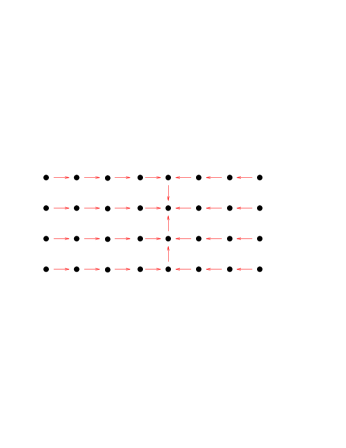
An additional feature of the pass-through modes is the ability to do arbitrary precision global sums efficiently. The SCU can continue to add the results of a previous 32-bit pass-through sum to the next pass-through sum. Since precision is most important in the global sums, we have the ability to easily insure that our global sums are accurate.
The SCU control registers are memory mapped into the DSP address space. A send operation to one of the eight neighbors requires the DSP to write to two SCU control registers. One write programs the DMA for this transfer with information about the number of blocks of data, the size of each data block and the offset between blocks. The second gives the starting address of the data to be sent and starts the send. Programming the receiving node is similar and also takes two writes.
3.2.2 Circular buffer
To achieve a balance between the DSP speed and the DRAM bandwidth, we have implemented a fetch-ahead cache, which we call the circular buffer (CIRBUF). The CIRBUF contains 32 words of memory, which it manages according to how it is programmed, and it can remember five different programming modes concurrently. Programming modes are generally set before entering a particular subroutine and fall into two general categories:
-
•
one wait-state modes: In these modes, every DSP read from memory takes at least two 25 MHz cycles. The CIRBUF is programmed to try and stay a few words ahead of the address of the last DSP read, to achieve as many two cycle reads as possible. The programmer does not need to worry about the pattern of fetches from memory; the CIRBUF will respond as quickly as possible no matter how the program jumps around. This mode is useful when running a general C program, for example.
-
•
zero wait-state modes: In these modes, the CIRBUF can provide a word from memory every 25 MHz cycle, after an initial delay of three cycles for the first word. To achieve this performance, the CIRBUF must know it already has any word it will be asked for. It can do this, since the programming mode contains information about the maximum difference in the addresses between consecutive requests.
For example, to read sequentially through an SU(3) matrix, as is necessary for a matrix times vector product, you will never jump ahead by more than one word beyond the previous word fetched. For the multiplication of the hermitian conjugate of this matrix times a vector, you would commonly skip ahead by five words and hence would use a different mode for the circular buffer.
Physical memory appears multiple times in the address space of the DSP. Reading the same physical memory under the control of different programming modes of the circular buffer is accomplished by reading a different image of memory. This involves the addition of a constant offset to the addresses of the data to be fetched.
The CIRBUF gives an obvious large speed increase compared to the three cycle reads that could be sustained from DRAM without its presence. We have also found it quite straightforward to write programs, where performance is important, using the zero wait-state modes
3.3 Node gate array
The SCU and CIRBUF discussed in the previous sections are implemented in an application specific integrated circuit (ASIC), called the node gate array (NGA) (Figure 3), which we have designed. The NGA also contains an interface to DRAM, which handles DRAM refreshes and incorporates a double-bit error detection and single bit error correction unit; a module to arbitrate DRAM access between the SCU, the CIRBUF and direct DSP reads; registers to latch and send global interrupts; and circuitry for clock synchronization and other boot-time issues.
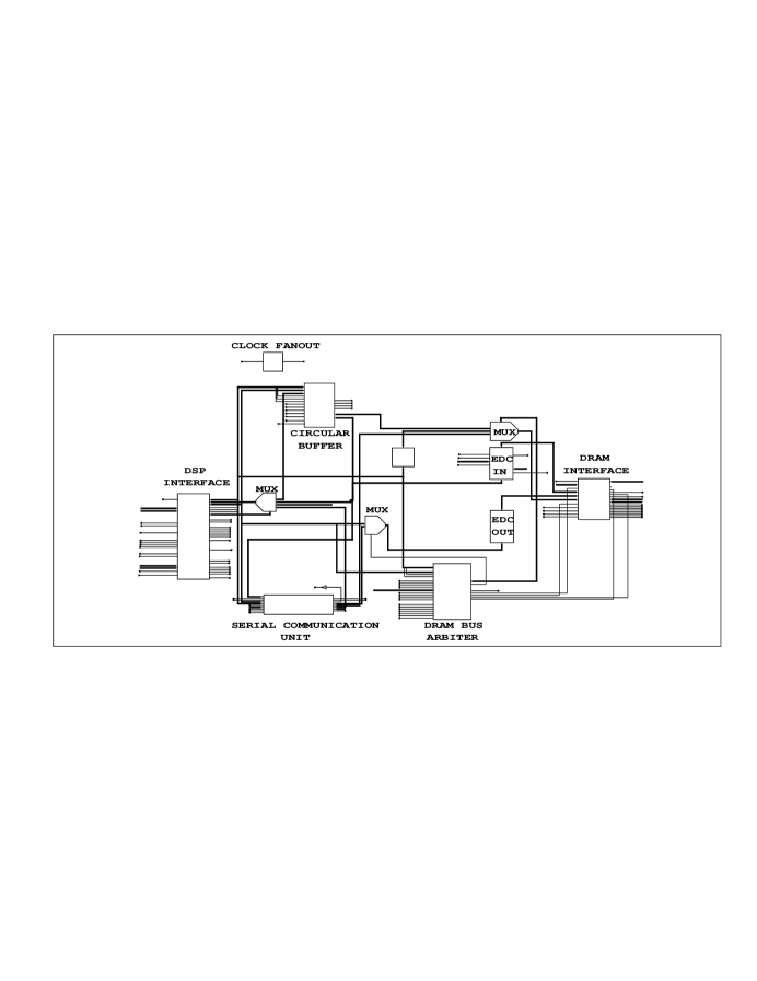
This is the one customized chip required for this project. It will have 208 pins and be about 1.25 inches on each side. The architecture has been implemented using a high-level hardware description language described elsewhere in these proceedings [2], which is then turned into schematics by a compiler-like tool called a synthesizer. We have a complete schematic representation for our NGA and are ready to send it to the engineering staff of an ASIC manufacturer for final testing and production.
3.4 Complete machine
We will attach 64 nodes of our machine to a motherboard using SIMM-like edge connectors, making it easy to replace a failed node[1]. On each motherboard, there will also be two SCSI ports for I/O to the host SUN workstation and a parallel disk/tape array. With over 5 Mbytes/sec bandwidth per SCSI port and 256 motherboards, the bandwidth to 256 disks is easily 1 Gbyte/sec (We expect to begin with 32 or 64 disks.).
Each motherboard will have a array of processors. Eight motherboards will be placed together in a commercial crate and 4 crates, separated by heat exchangers, will be stacked into a rack. Cabling can be done so that no cable is longer than about 6 feet.
3.5 DSP Tools
The DSP comes with a complete software development environment from TI, including assembler, C compiler, and a graphical debugger. Application code is also available from a TI bulletin board. As an example, when we needed to rearrange the compiler output for use as input to our NGA simulations, a subroutine was added to a bulletin board program.
In addition, we have a number of commercial DSP boards plugged into a SUN and various PC’s, permitting us to program on real hardware. In particular, one of the DSP boards (from DSP Research) has a SCSI port driven by the DSP, allowing development of the SCSI software for the connection between the 0.8 Teraflops machine and a SUN workstation.
Finally, we also have an emulator pod from TI which allows an external DSP to be completely controlled from a personal computer. This will be extremely useful when we have our first prototype hardware. The user controls the external DSP through a graphical interface that is the same as the interface to the simulator and debugger.
3.6 Software
We have gained considerable experience programming the DSP, using the various DSP boards. The TI software development tools are very robust and complete. We have also done extensive programming of the DSP and NGA assembly together, using the ViewLogic environment and the Logic Modeling model of the DSP[2]. This is part of the development and testing process for the NGA and is a gate level simulation of the NGA.
We currently have both a staggered and Wilson fermion conjugate gradient code running on our node, using the CIRBUF in zero wait-state modes and the SCU, without global sums. These programs have not only allowed us to gain experience in programming the machine for high performance, but have also caught many errors in our NGA design. The programs involve assembly-code subroutines to do the application of the Dirac operator, with C programs performing initializations and high level control. (Including comments, the staggered Dirac operator assembly code is about 1,000 lines long.)
The staggered conjugate gradient for a lattice, running on actual DSP hardware with SRAM (so there are no memory bandwidth delays), sustains 56% of peak speed. This same program on our node, using DRAM and the CIRBUF sustains 46%, showing that the CIRBUF is making the DRAM appear fast. A quick modification of the program to use the serial communication network (so we could test the NGA) achieves 30%, which should go to at least 40% with a little tuning.
The Wilson conjugate gradient code uses the DMA to load the DSP’s internal memory and sustains over 30% on a lattice. This performance will increase as the lattice volume per node increases. In addition, our simulator currently is running with an artificially rapid refresh rate for the DRAM, so we can look for errors in the DRAM controller. This degrades all our performance figures.
These results give a lower bound on the performance we can expect on the real machine. Our programming experience has also given us ideas about more efficient programming schemes.
3.7 Physics goals
The primary physics goals are quite clear; to do QCD simulations with as much control over errors as possible. Comparison of dynamical fermion and quenched calculations should reveal the accuracy or breakdown of the quenched approximation.
A second major goal of this project is to archive the configurations we produce for use by others. To this end we are implementing an archiving system on our current 256-node machine, which will grow to hold the configurations of the 0.8 Teraflops machine. These configurations will provide the community with a common set of lattices with known properties (lattice scale, hadron masses, etc.) and allow extraction of the full spectrum of physics available.
4 SUMMARY
The Multidisciplinary Teraflops Project has specified an architecture for the accelerator node, but must find a network to host it. About $1 million has been spent, with about $3.2 million needed for the completion of a few boards.
The Columbia 0.8 Teraflops computer has its NGA completely designed and
the first hardware is expected to be ready in a few months. Funding
has been acquired for a 512-node prototype with a request for funding
of the full machine to be made upon successful operation of the
prototype.
Acknowledgements: I would like to thank Estia Eichten, Andreas
Kronfeld and Don Weingarten for discussions and Richard Brower and John
Negele for providing detailed information about the Multidisciplinary
Teraflops Project.
References
- [1] I. Arsenin, et. al., Nucl. Phys. B34 (Proc. Suppl.) 820 (1994).
- [2] I. Arsenin, these proceedings.