Status of the QCDOC project††thanks: Presented by NHC and TW at Lattice 2001, Berlin.
Abstract
A status report is given of the QCDOC project, a massively parallel computer optimized for lattice QCD using system-on-a-chip technology. We describe several of the hardware and software features unique to the QCDOC architecture and present performance figures obtained from simulating the current VHDL design of the QCDOC chip with single-cycle accuracy.
1 INTRODUCTION
The debate over which computing platforms are suitable for the simulation of lattice gauge theories has continued at this year’s lattice conference. It has been shown that recent off-the-shelf PC processors by Intel or AMD are capable of delivering impressive floating-point performance on the order of 1 GFlops if the vector processing units are employed and cache management is optimized [1]. Unfortunately, this single-node performance cannot be fully utilized in a PC cluster if the local lattice volume becomes small. In this case, the surface-to-volume ratio is large, and the communications latency inherent in standard network solutions such as Ethernet or Myrinet slows down the individual processors. Therefore, to achieve reasonable efficiencies with a PC cluster, the local lattice volume must not be too small. This implies that for a given total lattice volume, the number of nodes working on a single problem is limited.
However, to finish a dynamical fermion calculation on a moderately large lattice in a reasonable amount of time, it is essential to distribute the total volume onto as many nodes as possible, which implies very small local lattice volumes, perhaps as small as . This requires communications between neighboring nodes with extremely low latencies that cannot be achieved using off-the-shelf networking components. Massively parallel machines with custom-designed communications hardware (with latencies 10–100 times smaller than in the case of Myrinet) appear to be the only viable alternative. This is especially true in the field of lattice gauge theory with its very regular communications requirements. In this contribution, we describe the design of the QCDOC architecture which is capable of delivering computing power in the tens of TFlops range at a price/performance ratio of 1 US-$ per sustained MFlops.
2 OVERVIEW OF QCDOC
A first description of the QCDOC project has been given at last year’s lattice conference [2]. In the nomenclature of parallel computers, this is a multiple-instruction, multiple-data (MIMD) machine with distributed memory. The name QCDOC stands for “QCD On a Chip”. An essential element of this project is the collaboration with IBM Research and the resulting ability to utilize IBM’s system-on-a-chip technology. Nowadays it is possible to integrate most of the components that make up a single processing node on a single chip, creating an application-specific integrated circuit, or ASIC. The QCDOC chip is such an ASIC, consisting of
-
•
500 MHz, 32-bit PowerPC 440 processor core
-
•
64-bit, 1 GFlops floating-point unit
-
•
4 MBytes on-chip memory (embedded DRAM)
-
•
controllers for embedded and external memory
-
•
nearest-neighbor serial communications unit with estimated latencies of 120ns (300 ns) for send (receive), overlapped between the 12 independent directions and an aggregate bandwidth of 12 Gbit/s
-
•
other components such as Ethernet controller, interrupt controller, etc.
The chip will occupy a die size of about , and the power consumption is expected to be in the range of 1–2 W.
Two such ASICs will be mounted on a daughterboard, together with two industry-standard double data rate (DDR) SDRAM modules (one per ASIC) whose capacity will be determined by the price of memory when the machine is assembled. (At the time of this writing, 256 MByte registered DIMMs with ECC were available for $40.) 32 daughterboards will be mounted on a motherboard, and 8 motherboards in a crate with a single backplane. The final machine then consists of a certain number of such crates.
There are two separate networks: the physics network and an Ethernet-based auxiliary network. The physics network consists of high-speed serial links between nearest neighbors with a bandwidth of 2500 Mbits/s per link. The nodes are arranged in a 6-dimensional torus which allows for an efficient partitioning of the machine in software, as described in detail in Ref. [2]. The serial-communications unit in the QCDOC ASIC provides direct memory access, single-bit error detection with automatic resend, and a low-latency store-and-forward mode for global operations. The auxiliary network is used for booting, diagnostics, and I/O over Ethernet, with an Ethernet controller integrated on the ASIC. The Ethernet traffic to and from the ASIC will run at 100 Mbit/s. Hubs or switches on the motherboard will provide a bandwidth of 1.6 Gbit/s off a motherboard to commercial switches and the host workstation.
3 THE QCDOC ASIC
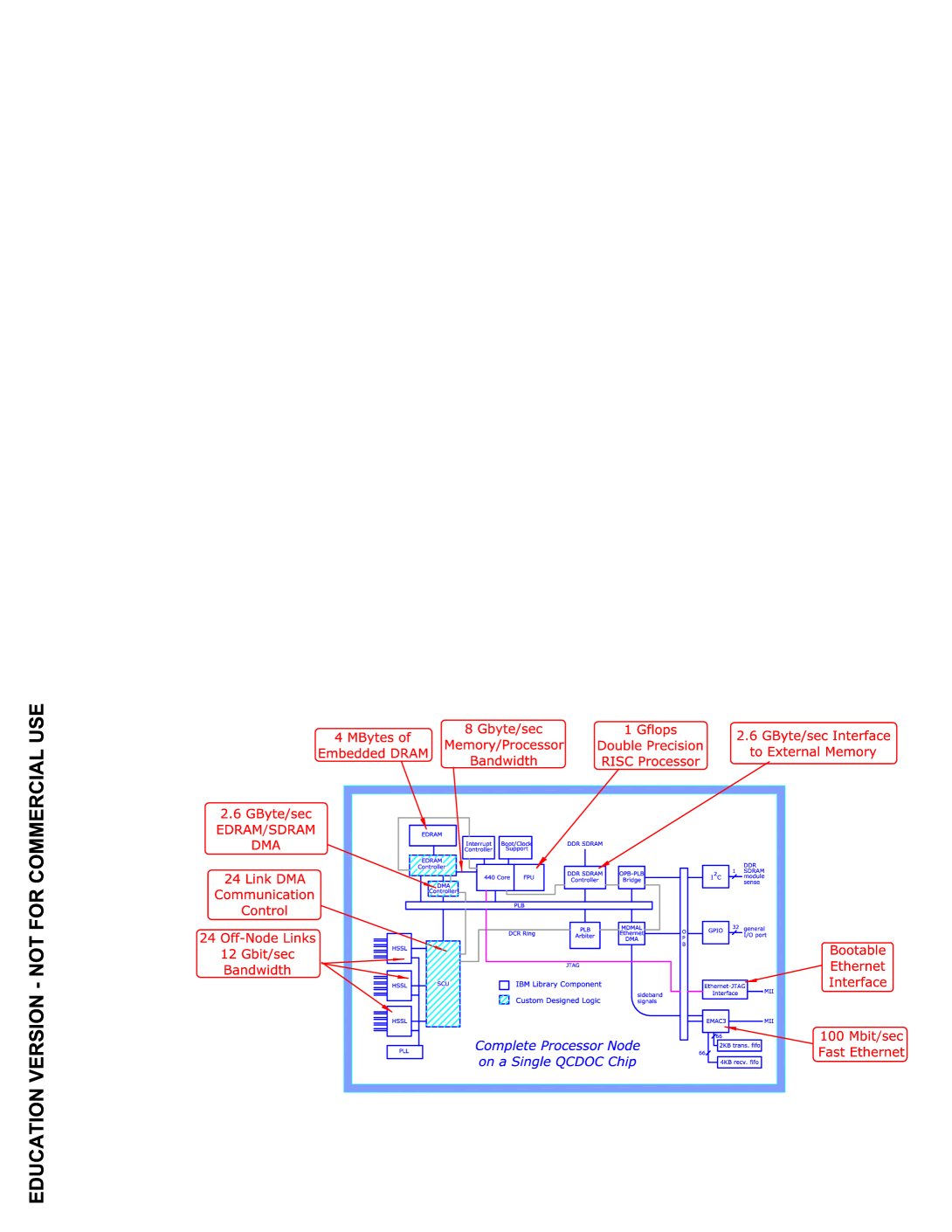
A schematic picture of the QCDOC ASIC is shown in Fig. 1. In this section we describe the various components in more detail. Many of the ingredients of the ASIC are provided by IBM, see Secs. 3.1–3.2. The major custom-designed components are the serial communications unit (SCU) and the prefetching eDRAM controller (PEC), see Secs. 3.3–3.4.
3.1 IBM Library Components
-
•
There are three main busses:
-
–
The processor local bus (PLB) is a 128-bit wide, fully synchronous bus that runs at 1/3 of the CPU frequency. It has separate read and write busses, supports pipelining (up to 4 deep), and has a large number of sophisticated features such as split transactions, burst transfers, etc.
-
–
The on-chip peripheral bus (OPB) is a 32-bit wide, synchronous bus running at 1/2 of the PLB frequency. Its basic purpose is to off-load slower devices from the PLB bus.
-
–
The device control register bus (DCR) is a slow and simple bus used to read and write control registers. The devices on this bus are connected in a ring-like fashion. The 440 is the only master on this bus.
-
–
-
•
The 440 PowerPC processor core is a dual-issue, superscalar, 32-bit implementation of the IBM Book-E architecture (the E stands for embedded). The core has a 7 stage pipeline. There are instruction and data caches of size 32 kBytes each. These are 64-way associative, partitionable, and lockable. Hardware memory protection is provided through a translation-lookaside buffer (TLB). The 440 has three PLB master interfaces, one each for instruction read, data read, and data write. The 440 will run at 500 MHz and is connected to a 64-bit, 1 GFlops IEEE floating-point unit (for details of the FPU see Ref. [3]). An important feature of the 440 is that it contains a JTAG interface. JTAG (Joint Test Action Group) is an industry-standard protocol that allows an external device to take complete control of the processor. This functionality will be used for booting and debugging, see below.
-
•
The PLB arbiter provides programmable arbitration for the up to eight allowed masters that can control PLB transfers. In our design we have seven masters: the three PLB master interfaces of the 440 (two of which, namely data read and data write, will be channeled through the PEC, see below), the MCMAL, two master interfaces for the send and receive operations of the SCU and one for the DMA unit.
-
•
The 4 MBytes of embedded DRAM (eDRAM) are a standard IBM library component that will be accessed with low latency and high bandwidth through a custom-designed controller, the PEC, see Sec. 3.4 below.
-
•
The Universal Interrupt Controller (UIC) processes the various interrupts generated on- and off-chip and provides critical and non-critical interrupt signals to the 440.
-
•
The DDR controller is a slave on the PLB, capable of transferring data to/from external DDR SDRAM at a peak bandwidth of 2.6 GBytes/s. It supports an address space of 2 GBytes and provides error detection, error correction, and refresh of the off-chip SDRAM.
-
•
The PLB-OPB bridge is used to transfer data between the two busses. It is the only master on the OPB and a slave on the PLB.
-
•
The Ethernet media access controller (EMAC) provides a 100 Mbit/s Ethernet interface. The media-independent interface (MII) signals at the ASIC boundary are connected to a physical layer chip on the daughterboard. The EMAC is a slave on the OPB and has sideband signals to the MCMAL on the PLB.
-
•
The DMA-capable Memory Access Layer (MCMAL) loads/unloads the EMAC through the sideband signals. It is a master on the PLB.
-
•
The inter-integrated circuit (I2C) controller is a slave on the OPB used to read the configuration of the DDR DIMM. This information is then used to configure the DDR controller.
-
•
The general purpose I/O (GPIO) unit is another slave on the OPB whose 32-bit wide data bus will be taken out to the ASIC boundary. It can be used, e.g., to drive LEDs.
-
•
The high-speed serial links (HSSL) used by the SCU each contain eight independent ports (four each for send/receive) through which bits are clocked into/out of the ASIC at 500 Mbit/s per port. The bits are converted to bytes (or vice versa) in the HSSL. The HSSL input clocks are phase-aligned by another IBM macro, the phase-locked loop (PLL).
3.2 Ethernet-JTAG Interface
As mentioned above, the 440 core has a JTAG interface over which one can take complete control of the processor. In particular, this interface can be used to load boot code into the instruction cache and start execution. This completely eliminates the need for boot ROM. The question is how the JTAG instructions should be loaded into the 440. (There are special tools that use the JTAG interface, but it would be impractical to connect one tool per ASIC for booting.) A solution to this question has already been developed at IBM Research, implemented using a field-programmable gate array (FPGA), that converts special Ethernet packets to JTAG commands and vice versa. This logic is now part of the QCDOC ASIC and will be used not only for booting but also to access the CPU for diagnostics/debugging at run time. The unique MAC address of each ASIC is provided to the Ethernet-JTAG component by location pins on the ASIC, and the IP address is then derived from the MAC address.
3.3 Serial Communications Unit (SCU)
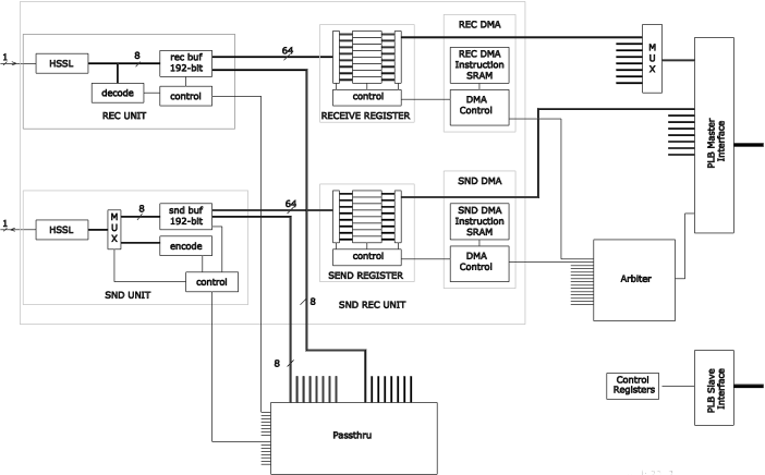
The task of the SCU is to reliably manage the exchange of data between neighboring nodes with minimum latency and maximum bandwidth. The design takes into account the particular communication requirements of lattice QCD simulations. A schematic picture of the SCU is shown in Fig. 2.
The custom protocol governing the data transfers defines packets that contain a 64-bit data word and an 8-bit header containing control and parity bits. When the receive unit receives a packet, it first interprets the header, buffers the bytes from the HSSL, and assembles the 64-bit word. It then transfers the word to the receive register or passes it on to the send unit. The receive buffer can store three 64-bit words so that the send unit (in a neighboring node) can send three words before an acknowledgment is received. The functionality of the send unit is essentially the inverse of that of the receive unit. Send and receive operations can proceed simultaneously. Each send or receive unit is controlled by a DMA engine which then transfers the data between memory and a send/receive register. Each DMA engine is controlled by block-strided-move instructions stored in SRAM in the SCU itself.
A low-latency passthrough mode is provided for global operations. Because of the latencies associated with the HSSL, the most efficient method to perform global sums is “shift-and-add”, using a store-and-forward capability built into the SCU.
The expected latency of a send (receive) operation is 120 ns (300 ns). This is one to two orders of magnitude lower than the latencies associated with Myrinet. Since a write instruction from the 440 can initiate many independent transfers on any subset of the 24 send or receive channels, the latencies associated with multiple transfers can be overlapped to some degree. The total off-chip bandwidth using all 24 HSSL ports is 12 Gbit/s. In a 4-dimensional physics application only 16 of the 24 HSSL ports will be used, resulting in a total bandwidth of 8 Gbit/s. This provides a good match for the communications requirements of typical applications. As a worst-case example, we consider a local lattice and the application of a staggered fermion conjugate gradient. In this case we obtain
| FPU alone | 75% efficiency |
| FPU + n.n. communications | 48% efficiency |
| FPU + n.n. + global sums | 38% efficiency |
The 75% efficiency in the first line is a reasonable assumption based on the performance figures quoted in Table 1 below.
3.4 Prefetching eDRAM Controller (PEC)
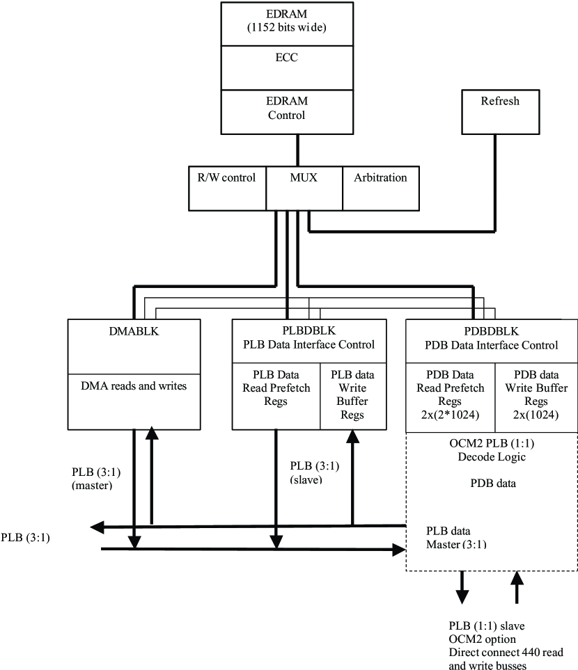
The PEC (shown schematically in Fig. 3) is designed to provide the 440 with high-bandwidth access to the eDRAM. It interfaces to the 440 data read and data write busses via a fast version of the PLB that runs at the CPU frequency and that we call processor direct bus (PDB). The PEC also contains a PLB slave interface to allow for read and write operations from/to any master on the PLB as well as a DMA engine to transfer data between eDRAM and the external DDR memory.
The maximum PDB bandwidth is 8 GBytes/s for read and 8 GBytes/s for write. The latency of the PDB itself is 1-2 CPU cycles. This very low latency eliminates the need for pipelining. The access to eDRAM (which is memory-mapped) proceeds at 8 GBytes/s. ECC is built into the PEC, with 1-bit error correct and 2-bit error detect functionality. The PEC also refreshes the eDRAM.
The read data prefetch from eDRAM occurs in two 1024-bit lines. Three read ports (PDB, PLB slave, DMA) arbitrate for the common eDRAM. The coherency between PDB, PLB slave, and DMA is maintained within the PEC. Each read port has four 1024-bit registers that are paired in two sets to allow for ping-ponging between different memory locations. There are also two 1024-bit write buffer registers each for the PDB/PLB slave/DMA write interfaces.
4 SOFTWARE
In this section the various aspects of the QCDOC software environment are described. Efforts are being made to make this environment user-friendly and to allow a wide range of application codes to run on the QCDOC platform without the need for extensive porting.
Boot kernel. The boot kernel will be loaded from the host work station via Ethernet using the reliable UDP protocol. The Ethernet-JTAG interface in the ASIC converts the packets to JTAG commands which in turn load the boot code into the instruction cache and start execution (see also Sec. 3.2). The boot kernel then assigns an IP address to the ASIC (based on the MAC address provided by the location pins) and loads the Ethernet driver.
Run-time kernel. The run-time kernel communicates with the host using the Ethernet driver loaded by the boot kernel. It performs complete node diagnostics and provides read, write, and execute capability. It is based on the UNIX RPC protocol.
RISCWatch debugger. This is an IBM-provided PowerPC development/debugging environment for a set of selected nodes. It provides single-stepping capability with an advanced, user-friendly graphical user interface showing a cycle-by-cycle display of the internal state of the PowerPC processor as OS or user code executes.
Extensive diagnostic programs. These will be provided to permit extensive, real-time hardware monitoring during program execution as well as targeted diagnostic tests for hardware maintenance.
Host Operating System. The host machine will be an SMP workstation with a suitable number of Gbit Ethernet ports, using a threaded transport protocol to efficiently manage tens of thousands of nodes. The host OS will manage both the boot and the run-time kernel operation. It will provide both a qcsh and a socket-based interface to the QCDOC operation, thus allowing for both csh-scripted and Perl-based machine control.
Disk software. We are planning a parallel disk system supporting a general distribution of disks. A simplified UNIX-like hierarchical file system will be used. A utility will be provided to store parallel files as a single, flattened, position-indexed file for archiving and use on other systems.
Compiler, linker, loader. The compiler and linker are GNU-based tools supporting C and C++ as well as Book-E compliant, PowerPC assembly language.
Lattice QCD application code. A code structure is being developed that will both provide the cross-platform capabilities needed by the UKQCD Collaboration and follow the QCD-API standard being developed by the U.S. SciDAC-supported lattice QCD software initiative.
5 STATUS AND PERFORMANCE
FIGURES
The functional design of the QCDOC ASIC is nearly finished. Single-node physics code is running on the VHDL simulator, and from these simulations we obtained the performance figures shown in Table 1. These all refer to double-precision calculations.
Table 1. Double-precision performance of single-node physics code running on the simulator.
| single node FPU, SU(3) 2-spinor | 84% of peak from L1 cache |
| 78% of peak from eDRAM | |
| cache fill/flush to eDRAM | 8.0 GB/s peak |
| 3.2 GB/s sustained (due to 440 latency) | |
| software visible bandwidth to eDRAM | 2.5 GB/s read, 2.0 GB/s write |
| DDR fill/flush | 1.2 GB/s read, 1.7 GB/s write |
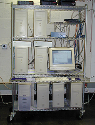
We have set up a test environment in which two nodes can successfully communicate in the VHDL simulator over their Ethernet interfaces and/or the HSSLs. The operating system is being developed on a system with six PowerPC 405GP boards, one PowerPC 750 board, five Ethernet-JTAG boards, and a RISCWatch probe. This hardware configuration is shown in Figure 4.
The current design has been successfully synthesized, and an analysis net list has been provided to IBM for floorplanning purposes. Anticipating a few iterations to satisfy timing constraints the complete design should be transferred to IBM by the end of 2001.
6 CONCLUSIONS
The QCDOC architecture combines state-of-the-art system-on-a-chip technology with custom-designed logic specially optimized for lattice QCD calculations to provide computing power in the tens of TFlops range at a price/performance ratio of 1 US-$ per sustained MFlops. Optimized QCD code is expected to run with an efficiency of roughly 50%. The communications latencies of the QCDOC design are one to two orders of magnitude smaller than those of commercial network solutions used in PC clusters, thus allowing for a large problem to be distributed onto many nodes. This fact, along with significantly lower power consumption, higher reliability, more compact packaging and a better price/performance ratio, motivates the design efforts that are required to construct such a supercomputer.
The first QCDOC machines with a combined peak speed of about 7 TFlops are projected to be finished in 2002, and by the end of 2003 the combined peak speed of QCDOC machines world-wide is targeted at 40 TFlops (10 TFlops of which will be installed in Edinburgh, 10 TFlops are planned for the RBRC and 20 TFlops for the U.S. lattice community).
ACKNOWLEDGMENTS
This research was supported in part by the U.S. Department of Energy, the Institute of Physical and Chemical Research (RIKEN) of Japan, and the U.K. Particle Physics and Astronomy Research Council.
References
- [1] M. Lüscher, hep-lat/0110007, these proceedings.
- [2] D. Chen et al., Nucl. Phys. B (Proc. Suppl.) 94 (2001) 825.
- [3] www.chips.ibm.com/products/powerpc/ newsletter/aug2001/new-prod3.html