apeNEXT: A MULTI-TFLOPS LQCD COMPUTING PROJECT
R. Alfieri, R. Di Renzo, E. Onofri
Dipartimento di Fisica, Università di Parma, and
INFN, Gruppo collegato di Parma, Parco Area delle Scienze, I-43100 Parma, Italy.
A. Bartoloni, C. Battista, N. Cabibbo, M. Cosimi,
A. Lonardo, A. Michelotti, F. Rapuano, B. Proietti,
D. Rossetti, G. Sacco, S. Tassa,
M. Torelli, P. Vicini
Dipartimento di Fisica, Università di Roma ‘La Sapienza’ and
INFN, Sezione di Roma, P.le A. Moro 2, I-00185 Roma, Italy.
Ph. Boucaud, O. Pène
Laboratoire de Physique Théorique
Université de Paris-sud (Orsay), France.
W. Errico, G. Magazzù, L. Sartori, F. Schifano, R. Tripiccione
INFN, Sezione di Pisa, Via Livornese 1291, I-56010 San Piero a Grado, Italy.
P. De Riso, R. Petronzio
Dipartimento di Fisica, Università di Roma II ‘Tor Vergata’ and
INFN, Sezione di Roma II, Via della Ricerca Scientifica, 1 - 00133 Roma,Italy.
C. Destri, R. Frezzotti, G. Marchesini
Dipartimento di Fisica, Università di Milano-Bicocca and
INFN, Sezione di Milano, Via Celoria 16, I-20100 Milano, Italy.
U. Gensch, A. Kretzschmann, H. Leich,
N. Paschedag, U. Schwendicke, H. Simma,
R. Sommer, K. Sulanke, P. Wegner
DESY, Platanenallee 6, D-15738 Zeuthen, Germany.
D. Pleiter, K. Jansen
NIC@DESY, Platanenallee 6, D-15738 Zeuthen, Germany.
A. Fucci, B. Martin, J. Pech
CERN, CH-1211 Geneva 23, Switzerland.
E. Panizzi
Dipartimento di Ingegneria Elettrica, Università de l’Aquila and
INFN, Sezione di Roma, P.le A. Moro 2, I-00185 Roma, Italy.
A. Petricola
Dipartimento di Ingegneria Elettrica, Università de l’Aquila and
INFN, Laboratori Nazionali del Gran Sasso, Assergi, Italy.
ABSTRACT
This paper is a slightly modified and reduced version of the proposal of the apeNEXT project, which was submitted to DESY and INFN in spring 2000. It presents the basic motivations and ideas of a next generation lattice QCD (LQCD) computing project, whose goal is the construction and operation of several large scale Multi-TFlops LQCD engines, providing an integrated peak performance of tens of TFlops, and a sustained (double precision) performance on key LQCD kernels of about 50% of peak speed. The software environment supporting these machine is organized in such a way that it allows relatively easy migration between apeNEXT and more traditional computer systems. We describe the physics motivations behind the project and the hardware and software architecture of the new LQCD engine.
1 Introduction
Several research groups in the Lattice QCD (LQCD) community have developed LQCD optimized massively parallel processors [1]. These systems have provided in the last decade a significant fraction of all compute cycles available all over the world for lattice simulations. In this framework, INFN and DESY have developed the APEmille parallel processor. APEmille is a LQCD oriented massively parallel number-cruncher [2], providing peak performance of several hundred Gflops. The first APEmille systems have been commissioned in late 1999. More machines have become available since then and yet a few more will be built in the near future (see later for details).
We expect APEmille machines to become the work-horse for LQCD computing in several laboratories in Europe in the next few years. It is however clear (and explained in detail in a following section) that APEmille is unable to support serious LQCD simulations at the level expected after the year 2003.
The continuing physics motivation to pursue numerical studies of lattice QCD and the level of needed computing resources have been analyzed in detail by a review panel appointed by the European Committee for Future Accelerator (ECFA) [3]. We fully endorse the conclusions of the ECFA report (which can be regarded as an ideal introduction to the present document). In this paper we present a proposal for a new lattice QCD project that builds on the experience of the previous generation APE machines and tries to implement several of the recommendations of the ECFA panel. This paper is an enlarged and improved version of a preliminary proposal [4], submitted to the INFN Board of Directors in summer 1999.
The new project (that we refer to as apeNEXT) is characterized by the following architectural goals:
-
•
an expected peak performance for large machines in excess of 5 TFlops, using double precision floating point arithmetics.
-
•
a sustained (double precision) efficiency of about 50% on key LQCD kernels (such as the inversion of the Dirac operator).
-
•
a large on-line data storage (512 GByte to 1 TByte for large machines).
-
•
input/output channels able to sustain a data-rate of MByte/sec/GFlops.
-
•
a programming environment that allows relatively straightforward and easy migration of physics codes between apeNEXT and more traditional computer systems.
From the point of view of the organization of the project, the following points are in order:
-
•
the apeNEXT architecture will be very closely optimized to LQCD simulations. In other words, apeNEXT will be more tuned towards LQCD than APEmille.
-
•
The general know-how of APEmille, as well as several important building blocks, will be heavily reused in the new project (properly rescaled to keep technology advances into account). This is a key point that we plan to leverage on, in order to shorten development time.
-
•
We plan from the beginning the installation of several large machines at approximately the same time at several collaboration sites. (Collaboration membership is also somewhat enlarged in comparison with APEmille). Stated otherwise, we plan to build up very high processing performance for LQCD (of the order of several tens of TFlops) by operating in a loosely coordinated way several machines.
-
•
Provisions to facilitate an industrial exploitation of the project are not one of the stated goals of the project. We do see however that several building blocks of the project (most notably in the area of inter-node communications) may have an important impact on other areas of computing for physics (and, more generally, for cluster computing or farming). We will do our best to make our results reusable.
This paper describes the hardware and software architecture that we plan to develop. It does not cover the organization of the project, the proposed schedule of our activities and any financial issues. These points are considered elsewhere. The paper is organized as follows:
-
•
Section 2 discusses the physics goals of the project and their corresponding computing requirements (in terms of processing performance, data storage, bandwidth).
-
•
Section 3 briefly summarizes the APEmille architecture and substantiates the need for a new project.
-
•
Section 4 reviews similar planned or started projects.
-
•
Section 5 surveys the status and prospects of some enabling technologies for our project.
-
•
Section 6 discusses advantages and disadvantages of custom versus off-the-shelf technologies for the processing element of the new computer.
-
•
Section 7 presents the global architecture of our new massively parallel LQCD machine.
-
•
Section 8 describes the details of the processing node.
-
•
Section 9 covers the architecture of the interconnection network.
-
•
Section 10 discusses several possible options for the topology and the mechanical set-up of the system.
-
•
Section 11 is the first section on software. Here we describe the programming environment that we plan to develop for apeNEXT.
-
•
Section 12 is a matching section discussing the operating system and other system-software issues.
-
•
Section 13 reviews the design method that we plan to follow in the development of the system.
-
•
Section 14 contains our conclusions.
2 Physics Requirements
In the definition of the new project we keep a clear focus on a very limited number of important physics simulation areas, that set the requirements for the new project.
The translation of physics requirements into machine parameters requires certain assumptions about the algorithms to be used. We base our considerations on tested algorithms such as SSOR-preconditioned BiCGstab and Hybrid Monte Carlo, for Wilson fermions with improved action [5]. New theoretical developments (domain wall fermions, Wilson-Dirac operators satisfying the Ginsparg-Wilson relation, etc.) are likely to be implemented in a way which has computational characteristics very similar to the standard Dirac operator.
We expect that in the years 2003-2006, large production LQCD simulations will be mainly focused on the following lines:
-
•
full QCD simulations (including dynamical fermions) on lattices with sizes of the order of (a physical system of fm and fm). Dynamical quark masses should also decrease, with a reasonable target corresponding to (although it is not realistic to expect that both goals are obtained in the same simulation).
-
•
simulations in the quenched approximation on very large lattices () and large ( fm and fm) for the study of physics with as little extrapolation as possible in the mass of the heavy quark.
The first item is heavily CPU limited, since one has to solve the Dirac equation repeatedly during the updating process. The second item is basically memory limited, due to very large lattice size. In both cases, our target is a resolution about two-times better than currently possible (implying, as discussed later on, an increase in computing power of two orders of magnitude).
As a guideline to define a new LQCD engine for these classes of problems, we require that:
-
1.
The node-topology and communication network is optimized for the lattice sizes required in full QCD simulations. Since for many problems of LQCD it is important to perform a finite-size scaling analysis, it is desirable that the machine performs efficiently not only on large but also on comparatively small lattices, e.g., in full QCD one may think of lattices with and 48, and . For smaller lattices, as the required computing performance decreases, more traditional machines (such as PC clusters) or previous generation dedicated systems can be used.
-
2.
The communication network has enough bandwidth to handle the large degree of data exchange between neighbouring sites (and hence compute nodes) needed in LQCD computations. The interconnect architecture should support the natural (APE-like) programming model with direct remote data access [6]. This approach minimizes software and memory overhead (and coding effort) for pre-loading of remote data.
-
3.
The processing nodes sustain high performance on the execution of the arithmetic and control operations which are relevant for the codes (or at least their basic kernels) of full-QCD algorithms, in particular double precision floating point arithmetics, memory access to field variables of composed data structures, local and global program-flow control, etc.
To obtain a good floating-point efficiency for the execution of a given computation, the compute power and memory bandwidth should be balanced accordingly. This balance is usually measured in term of the parameter , defined as the ratio between the number of floating-point operations and the corresponding memory accesses (in the corresponding data format). A processor is balanced for a given algorithm if the value required by the algorithm is roughly equal to the value allowed by the processor itself. In the case of the Dirac operator, which usually dominates the cost in LQCD computations, a typical value is .
-
4.
Memory size, disk space and disk-bandwidth match each other and are well suited to the problems we want to study. This means that all compute intensive kernels must not be slowed significantly because required data is not available in main memory. We must keep all data in physical memory as long as possible. In all cases in which this is not possible (e.g., for light-fermion propagators on very large lattices) we must be able to temporarily store on (and retrieve from) disk with large enough bandwidth.
These requirements shape the global architecture of the machine:
-
1.
We consider architectures based on three dimensional grids of processors, with nearest neighbour data-links. Reasonable sizes of the mesh of processors that will be used for the simulation of large lattices are somewhere in the range nodes, where a physical lattice of points can be readily mapped. For finite size analysis on small lattices, a mesh of processors may be considered.
The size of the processor mesh dictates a lower bound on the communication bandwidth between neighbouring processors. We define by the ratio of local memory accesses (transfers between processor and its memory) over remote memory accesses (transfers between neighbour processors), which depends on the lattice size and the algorithm. Under the assumption of balanced local bandwidth (i.e., processors are able to access enough data in local memory to sustain their potential performance, see later for details), effective bandwidth111 including the effect of the start-up latency for typical packet lengths. for remote communications must not be lower than times the local bandwidth. Estimates of the required ratio for a naive implementation of the Dirac operator using Wilson fermions are given in table 1 for a sub-lattice of physical points and local time direction per processor (note that, to first approximation, ).
Linear lattice size Table 1: Local vs. remote memory access patterns: is the ratio of memory accesses to local memory over memory accesses to neighbour nodes in a simple implementation of the solver for the Dirac operator. is estimated as a function of the linear size of the sub-lattice mapped onto each processor. A nice and simple trick can be used in the computation of the Dirac operator to reduce the number of remote accesses. For the negative directions the Dirac operator involves terms of the type where the fermion term and the corresponding gauge matrix () must be fetched from the same place. We can therefore evaluate the product on the remote node and transfer the result only. In brief, all remote accesses involving gauge fields disappear. Table 2 contains the values corresponding to the evaluation of the Dirac operator using the above mentioned technique. We consider the comfortably increased values as an useful safety margin, that could be exploited to increase the floating point performance of each node, at fixed remote bandwidth.
Linear lattice size 11.25 9 Table 2: Local vs remote memory accesses: this table is the same as the previous one, except that is estimated taking into account the trick, described in the text, that reduces remote accesses. The last two entries refer to non-square sub-lattices that might be used when simulating a lattice of spatial size on large machines with or nodes. Clearly the actual values of which can be accepted must be studied more carefully (possibly simulating architectural details of the mechanisms that hide remote communications)
-
2.
To discuss memory-size requirements in more details, one has to distinguish between the case of full QCD simulations and calculations in the quenched approximation.
In full QCD simulations, by far the largest amount of time is spent in the updating process. In this case, on-line memory has to be large enough to allow for the implementation of efficient algorithms. State-of-the-art update algorithms need a large number of auxiliary fields on each lattice site. We use as unity the amount of memory associated to one fermion field (24 data words, corresponding to 192 Bytes in double precision. We call this quantity a fermion equivalent - feq - in the following). A generous estimate, leaving space for more sophisticated, presumably more memory intensive algorithms, is about feq per site.
On the other hand, in the case of the quenched approximation, the updating process may be neglected for both computing power and memory requirements (less than feq per lattice site are needed). Instead, we have to consider the memory requirement originating from the measurement of a heavy-light form-factor. The database needed for such a calculation consists of one gauge field configuration, one Pauli term, fermion propagators ( and are the numbers of heavy and light fermions respectively), each replicated for the number of momenta and operator insertions used and for each lattice site (typical cases, being , 3 momenta and one operator insertion). Quenched QCD will be used essentially for heavy quark phenomenology. Here the real problem is the extrapolation to the quark mass. To be safe one should have a physical cutoff much larger than the masses that enter the simulation. Then large lattices, of the order of , are necessary.
gauge fields 72 W 3 feq fermion propagator 288 W 12 feq (pseudo-) fermion field 24 W 1 feq Pauli term for improvement 72 W 3 feq Table 3: Data structures used in LQCD and corresponding memory requirements (in words and fermion equivalent storage) per lattice point. Greek indices run from to and Latin indices from to . The first three entries are general complex matrices, while the Pauli term is hermitian: . We summarize our memory requirements in table 3 (where the size of the relevant data structures are presented) and in table 4, where actual memory sizes are collected, under the assumptions of using double precision222The necessity of double precision arithmetic in full QCD has been investigated in the literature [7] and will not be discussed here. throughout. From the first two lines of table 4, we see that we cannot expect to keep the whole data-base in physical memory when large lattices are considered. However, if only two propagators at the time are kept in memory, for ease of programming, while the others are either recalculated (the heavy ones) or stored and reloaded from disk (the light ones), memory requirements reduce sharply (third line in the table).
We conclude that, by judiciously swapping data to disks, a memory size of the order of TByte is a good compromise for both our case studies. Alternatively, one might consider two memory options: a small memory machine ( GByte) for full QCD and a large memory version ( TByte) for quenched studies.
Case updating measurement small lattice, full QCD G T large lattice, quenched QCD G T large lattice + disk G T Table 4: Total memory requirements for the case studies discussed in the text. The line labeled + disk refers to the case in which two propagators only are kept in memory (all others being swapped onto disk or recomputed). -
3.
Fast input-output is mandatory, as obvious from the previous point, for studies on large lattices. As a rule of thumb, we may want to load or store one (large lattice) propagator ( 250 GBytes) in little more than one minute. This requires a global bandwidth of the order of GBytes/sec.
For full QCD permanent storage of the configurations is required due to the computing effort needed to generate them. This is a storage-density (as opposed to bandwidth) problem which is independent of the machine architecture and should be discussed in a different context, with potential links with the GRID [8] project, likely to be supported by the European Commission. In the case of large lattices in quenched QCD the strategy of computing on the fly without saving configurations is the best. Only the final correlation functions are saved and this means at most a few tens of MBytes per configuration.
Processing performance is strictly speaking not a clear-cut requirement: the more is available, the better. We can estimate how much is enough, however, by extrapolating the present state of the art. A sustained performance of 300 GFlops (with perhaps 40% efficiency) is now heavily used for full QCD simulations on lattices of size [9]. If we assume a critical slowing down where computer time grows like [10], we would like to have a sustained performance two orders of magnitude higher if we want to halve .
An ambitious target for our project is therefore a total installed performance in the order of TFlops. From the point of view of physics requirements, it is not important that this computing power be sustained on a single system. Several smaller machines can perform equally well (or perhaps better), as long as each of them is able to handle large enough lattices.
Also, we must envisage the operation of some lower performance (and correspondingly smaller memory) machines, where small lattices are handled and algorithms, programs and physical parameters are tuned before a large calculation is moved onto a large production machine.
3 The APEmille Project
In this section we briefly review APEmille.
APEmille is the present generation APE project. It is based on the standard structure of a large array of processing nodes arranged at the edges of a three dimensional mesh and operating in SIMD mode.
At present (November 2000), several medium-size installations are up and running, while several larger units are under construction (see table 5). Considering all large and small machines, the integrated peak performance available at the end of the year 2000 will be about 1 TFlops at INFN and about 400 Gflops at DESY. The largest single system will have a peak performance of 250 (possibly 500 Gflops). Other institutions in Europe are procuring (or considering to procure) APEmille machines.
| Site | peak performance | status |
| Rome | 260 Gflops | running |
| Zeuthen | 130 Gflops | running |
| Rome II | 65 Gflops | running |
| Bielefeld | 80 Gflops | running |
| Milano/Parma | 130 GFlops | planned, Dec. 2000 |
| Pisa | 130 Gflops | planned, Dec. 2000 |
| Rome II | + 65 Gflops | planned, Dec. 2000 |
| Rome | + 260 Gflops | planned, Dec. 2000 |
| Zeuthen | + 260 Gflops | planned, Spring 2001 |
In a typical critical LQCD kernel (a solver for the Dirac operator) coded in the high level TAO programming language, measured sustained performance in single precision is about 44% of peak performance and in double precision it is about 19% of peak single precision (i.e. 80% of peak performance in double precision). Higher efficiency can be obtained with more careful programming: we have pushed single precision performances up to about 58% of peak speed writing the key portions of the Dirac solver in assembly.
In a later section, we will claim that an architecture à la APEmille continues to be a very good choice for LQCD computing. We see however a number of problems in APEmille, all pointing to the development of a new generation system:
-
•
Peak Performance APEmille machines can be made larger than we plan to build, but not too large. The largest system that can be assembled with the present hardware building blocks is a configuration of nodes, corresponding to 1 TFlops peak performance (APEmille systems can be configured in principle as arrays). Still larger systems would need some minor hardware development and would probably be not convenient in LQCD, since they have an unordinately large number of nodes along one dimension.
-
•
Memory Size The very large APEmille machine described above has 64 GBytes memory. This is still several times lower than discussed in the section on requirements.
-
•
Floating-point precision APEmille is basically a single precision machine (performance decreases by factors from 2 to four in double precision). However, in future large LQCD simulations double precision will be necessary in an increasing number of cases.
-
•
Little space for improvements APEmille is architecturally very simple, since it relies on accurate and rigid hardware synchronization. This style of synchronization is difficult to support if the system clock is increased significantly. For this reason, we see little space for incremental improvements in performance.
4 A Review of Similar Projects
In this section, we gather some information on similar projects, carried out by other groups. To the best of our knowledge, the following activities are in progress:
-
•
CP-PACS
The CP-PACS collaboration have made a feasibility study of a future project which follows the CP-PACS project. Extrapolating the data of the performance obtained in recent full QCD simulations on the CP-PACS computer, they have estimated the computer time required for a large-scale full QCD calculation, with the quality of data comparable to that of the present quenched QCD study on the CP-PACS. They assume that lattice action and the simulation algorithm are identical to the present simulation on the CP-PACS. Their estimate, 100 TFlops year [11], is somewhat larger than the one of the ECFA panel. In addition to their feasibility study, CP-PACS are carrying out basic research on the following two topics, that they consider as very important technologies for the next-generation of massively parallel computers:
-
–
Development of an architecture of high-performance memory-integrated processor for the next generation massively parallel computers.
-
–
Establishment of a model of parallel I/O, parallel visualization and man-machine interface, which can process efficiently and flexibly the enormous amount of data generated by massively parallel computers.
CP-PACS hope they will have a chance to develop a next-generation computer using the results of their basic research in the near future, but they do not have a project at the present time.
-
–
-
•
Columbia The Columbia group have officially embarked on the design and construction of their next machine [12]. The design effort is still on a fairly high level with choice of processor and communications technology being the first questions that have been resolved. Most significant is the choice of microprocessor, which is provided by an IBM PowerPC core. This follows from an arrangement with IBM that permits to exploit proprietary technology to construct a full processing node (memory included) on a single chip. This feature provides the name to the new project QCD on a Chip (QCDOC). The node will contain a PowerPC 440 core, one 64-bit, 1 Gflops FPU (an integrated part of the PowerPC architecture), 4 MBytes of embedded DRAM and 8 bi-directional serial inter-processor links, each operating at 0.5 Gigabits/sec. If they are able to achieve this frequency, this would give a total off-node communications bandwidth of 1 GBytes/sec.
The group is now busy to determine the other details of the project and begin the detailed design of the node.
We also include an arbitrary selection of two (out of the many) interesting examples of PC-based cluster architectures for comparison.
-
•
The Wuppertal Cluster ALiCE
The ”Institut für Angewandte Informatik” at Wuppertal University has installed the first half of the Alpha-Linux-Cluster-Engine (ALiCE) in 1999. When the system is fully installed, in May 2000, it will consist of 128 DS10 uni-processor workstations connected by a Myrinet multi-stage crossbar switch. All CPUs will be upgraded to 600 MHz Alpha 21264 EV67 chips with 2 MBytes second level off-chip cache [13].
The cluster is intended to perform efficiently in several HPC application profiles at the University of Wuppertal, including computational chemistry, electrical engineering, scientific computing and simulations of quantum field theories.
Of particular interest is the operability of this self-made system in a University’s multi-user environment. In computer lab courses, the emphasis is on ”Physics by High Performance Computers”. Several student groups use the system simultaneously in interactive mode much alike a desk-top system.
A forward looking ALiCE-project, to be carried out together with the developers of the ParaStation communication software from Karlsruhe university, deals with optimization of efficiency and data organization for ALiCE under real life conditions, in particular with the goal to make parallel I/O and file system functionalities available.
-
•
PMS, The Poor Man’s Supercomputer A PC cluster has also been developed at Eötvös University in Budapest [15]. The current version of PMS has 32 PC’s. Contrary to the previous example, the PMS project has developed QCD-optimized communication hardware. They use dedicated add-on boards to establish physical communications between nearest neighbour PC’s in a three dimensional array. The actual configuration of 32 PC’s can be imagined as a mesh of processors. The system uses a standard Linux operating system and the favoured programming style is the well tested SIMD paradigm.
The present version of PMS is shaped by the requirement to reduce costs as much as possible. Indeed, PMS uses cheap AMD K6-2 processors (delivering only 225 MFlops each) while the special purpose communication interface has a bandwidth of just 2 MBytes/sec. We consider the PMS as a very good trade-off between the advantages offered by the use of general purpose systems and the performance boost that dedicated hardware is able to provide.
-
•
The MIT-Jefferson Lab project This project is organized in two phases. Phase I has been submitted to DOE in march 1999 [14] for a 256-processor cluster at JLab and a 64-processor cluster at MIT. The building block is a 4-processor Compaq SMP node with a MHz Alpha 21264 chip, MB cache/processor and Gbyte memory/SMP. The communication network is based on Myrinet switches. They plan to achieve a cost per sustained MFlops lower than $. The collaboration currently operates a 12 node prototype cluster equipped with 667 MHz Alpha 21264 at MIT. They plan to complete phase I by 2001. The collaboration has a quite intensive physics program mainly devoted to nucleon structure. Phase II of the project, not approved yet, foresees, in the years 2002-2005, multi-Teraflop machines from a combination of QCDOC and clusters. They are collaborating with Compaq to explore resources available at that time (EV7 and EV8).
5 Technological Scenarios
In this section we discuss forecasts about the state of the art for several enabling technologies in the years 2001-2002. We cover the following points:
-
1.
basic digital VLSI technology.
-
2.
memory technology.
-
3.
data-links.
-
4.
Off-the-shelf processors.
-
5.
The Crusoe architecture.
We conclude the section with a discussion of the architectural implications of the technology-driven choice of overcoming the strictly synchronous operation of APE100 and APEmille.
5.1 VLSI Technology
APEmille is based on a chip-set designed with a digital CMOS technology. A second source for the chip-set has been established, using a more advanced technology. In the next few years, and CMOS technologies will be readily available.
A comparison of some key features of the silicon technologies used in APEmille and of a representative of both and technologies is made in table 6.
| Feature | ES2 | Alcatel | UMC | UMC |
|---|---|---|---|---|
| 3.3 V | 3.3 V | 2.5 V | 1.8 V | |
| Gate delay | 180 ps | 100 ps | 75 ps | 36 ps |
| Gate density | K/mm2 | K/mm2 | K/mm2 | K/mm2 |
| Memory (1P) | Kb/mm2 | Kb/mm2 | Kb/mm2 | Kb/mm2 |
| Memory (2P) | Kb/mm2 | Kb/mm2 | Kb/mm2 | Kb/mm2 |
| Power/gate | W/MHz | W/MHz | W/MHz | W/Mhz |
The figures quoted in the table refer to processes that are (or will be) readily available through the same European silicon broker that helped us develop the second source of the APEmille chip set.
Let us consider a scaled version of the APEmille processor. If we use a process, it should be easy to reach a clock speed between three to five times higher than in APEmille, while we may expect to squeeze up to 9 times more transistors onto the same silicon area. We can stay on the safe side planning to use a clock frequency of MHz. An LQCD optimized processor running at this clock frequency with one floating-point pipeline would peak at 1.6 Gflops , using the well known normal operation , performed on complex operands. A chip three times more complex than J1000 (and three times faster) would dissipate less than two times more power.
5.2 Memory Technology
We limit ourselves to memory systems used in future high-end PC’s or low-end workstations. This choice (the same as APE100 and APEmille) should be the most effective to provide the highest level of integration, reduce costs and guarantee part availability.
In the near future, planned memory systems are either RAMBUS DRAM’s or DDR SDRAM’s.333In the following we do not distinguish between traditional DDR SDRAM and new “flavour” DDR SDRAM like Sync-Link because both are evolutionary designs of the same basic structure.
The DDR SDRAM (Double Data Rate Synchronous DRAM), is the evolution of the mature SDRAM (Synchronous DRAM) technology (widely used in the APEmille machine). The SDRAM is a low latency burst oriented device made of multiple (2 to 4) banks of asynchronous DRAM controlled by a synchronous controller which allows pipelining of the I/O interface (one word is accessed for every clock cycle). The Double Data Rate architecture realizes two data transfers per clock cycle using both edges of the clock and one special reference signal to fetch corresponding data.
The RAMBUS is a more advance memory architecture which works as a chip-to-chip system-level interface rather than a conventional memory device. The RAMBUS RDRAM (which stands for RAMBUS Direct Dram) shares the same architectural idea of the SDRAM one, a core asynchronous plus a synchronous controller. It makes use of a large degree of parallelism (32 interleaved memory banks) on a narrow internal bus. The RAMBUS RDRAM is based on the Direct RAMBUS Channel, a high speed 16-bit bus at a clock rate of 400 MHz, which thanks to the adoption of a dedicated signalling technology (RAMBUS Signalling Level) allows 600 MHz to 800 MHz data transfers.
In table 7 we summarize the main features of the two technologies, for currently available and next generation (less than 2 years from now) chips.
| DDR | RDRAM | DDR | RDRAM | |
|---|---|---|---|---|
| Data rate | 200 MHz | 800 MHz | 400 MHz | 800 MHz |
| Memory size | 256 Mbit | 128/144 Mbit | 1 Gbit | 256 Mbit |
| Organization | x4,x8,x16 | x16,x18 | x16,x32 | x16,x18 |
| Peak bandwidth | 0.4 GB/s (x16) | 1.6 GB/s | 1.6 GB/s (x32) | 1.6 GB/s |
| Package | TSOP(66) | BGA | TSOP(80) | BGA |
| Power (VCC) | 2.5 V | 2.5 V | 1.8/2.5 V | 1.8 V |
| I/O type | SSTL2 | RSL | SSTL (?) | RSL (?) |
| Power cons. | 80 mA | 330 mA | ? | ? |
| Cost (norm.) | 1.0 | 1.8 | ? | ? |
| Sample/Prod. | Now/Now | Now/Now | 3Q99/4Q00 | ? |
Some comments are in order:
-
•
The simple architecture of the DDR SDRAM allows larger memory size per device. For a given fixed amount of memory, this reduces the number of used components.
-
•
Since power consumption is proportional to the interface clock (a factor 4 between RAMBUS e DDR), aggregated memory systems using the DDR SDRAM reduce the global consumption.
-
•
On the other hand the extremely high peak bandwidth of the RAMBUS allows to build a very fast memory system with minimum impact on board space occupancy (compact BGA packaging).
-
•
The logic complexity of a RAMBUS interface is much larger than for a DDRAM controller (the latter could be easily designed on the basis of the experience done in the realization of the APEmille memory controller). On the other hand, several silicon foundries make a RAMBUS controller available as a core cell.
We conclude this section by presenting in table 8 two possible DDRAM-based memory systems for apeNEXT. The performance target is set by our basic performance figure, discussed in the previous subsection of and , leading to a bandwidth requirements of at least GBytes/sec (assuming double precision data words throughout).
| chip-size | 1 Gbit | 1 Gbit |
|---|---|---|
| chip organization | 32 bits | 32 bits |
| chip number | 4 | 2 |
| word size | 128 bit | 64 bit |
| bank size | 512 MBytes | 256 MBytes |
| frequency | 300 MHz | 400 MHz |
| total bandwidth | 4.8 GBytes/sec | 3.2 GBytes/sec |
| power consumption | 640 mW | 400 mW |
In conclusion, forthcoming memory technology is adequate to support the processor performance discussed above. There is in fact reasonable space to consider either fatter node processors, or multi-processor chips.
5.3 Data-link Technology
We now consider remote communications which, in our opinion, is a key technological challenge for the project.
Assuming our reference figures - 1.6 Gflops per node, along with , and (as defined in the previous sections) - we require an inter-processor communication bandwidth of about 400 MBytes/sec. As discussed above, several code optimization steps are able to reduce the amount of data to be transferred. The overlap between computation and communication can also be increased. All this steps reduce bandwidth requirements. We will stick however to the previous figure, so a large safety margin is established.
The needed communication patterns are however very simple: communications are needed between nearest-neighbours (L-shaped paths, between next-to-nearest neighbours are also useful) in a 3-d array of processors, where each processor has 6 direct links to its nearest neighbours. The real challenge in this area is therefore more the implementation of a fast, reliable and cheap link than the development of any clever routing strategy.
In APE100 and APEmille, links use large, parallel and synchronous data paths. Data words are injected at the transmitting end of the line following a rising transition of the clock and are strobed into the receiving end of the line at the next rising edge of the clock. This works if
| (1) | |||
| (2) |
where is the travel time over the physical link, is the clock period and is the phase spread between (nominally aligned) clock signals at various places in the machine. The conditions are met in APEmille, where , and , while they become clearly unrealistic for frequencies of MHz.
More advanced (high bandwidth) link technologies have recently become available, in which data and timing information are both encoded on the physical link, so asynchronous operation is possible. In the bandwidth range relevant for us, we have considered three different options:
-
•
Myrinet-like links. The physical layer of the Myrinet interconnect uses low swing single-ended signalling. One byte is encoded onto ten signal lines, carrying also timing information. The full duplex link uses two such busses. The present generation Myrinet link has a bandwidth of 160 MBytes/sec (using both edges of an 80 MHz clock), while a new generation (Myrinet-2000, 320 MBytes/sec) is under test. The main advantage of Myrinet links is that they pack a lot of bandwidth while keeping operating frequency low. Board layout details, connectors and cables are also very well tested. We are informally discussing with Myricom the possibility to use this link for apeNEXT. Myricom have agreed to allow us to use the link level (SAN-port) circuitry for their latest Myrinet chips (Myrinet 2000) as a basis for the apeNEXT links. Under a suitable non-redistribution agreement, Myricom will make available to the collaboration the layout of the basic cells, along with their Verilog models.
-
•
LVDS based links. The Low Voltage Differential Signalling (LVDS) technology is now widely used in many telecom and network technologies, like the Scalable Coherent Interface (SCI). LVDS is designed to work up to MHz. Several redundant encoding schemes (e.g., 8 bits into 10 bits) have been proposed. LVDS cells are readily available from several silicon vendors. New generations FPGA chips have been announced including LVDS options. Work is in progress to test LVDS links, as described later in this document.
-
•
High speed proprietary links. Several silicon houses (e.g., Texas Instruments (TI), National Semiconductor(NSC), LSI Logic) have developed very high speed proprietary links, aimed at the Gb Ethernet, Fiber-Channel, Infini-Band markets. The typical bandwidth is higher than 1 Gbit/s. Complete encoding-decoding black-boxes are usually available. This option has two main drawbacks: it makes the whole project dependent on a specific silicon house, and requires very careful layout of the printed circuits and proper choices of cables, connectors and the like.
Basic figures of the three options are compared in table 9, where we use for the LVDS case a more conservative frequency of 400 MHz.
| Technology | Frequency | Pins | Bandwidth | Power Dissipation |
|---|---|---|---|---|
| Myrinet | 160 MHz | 20 | 320 MBytes/s | 300 mW |
| LVDS | 400 MHz | 40 | 400 MBytes/s | 200 mW |
| SerDes(TI) | 1.24 GHz | 10 | 400 MBytes/s | 400 mW |
| NSC DS90CR483/484 | 784 MHz | 18 | 672 MBytes/s | 1500 mW |
An important issue is the reliability of the network, usually measured in BERR (average number of errors for transmitted bit). If we require fault-less operation of a large machine for one day (say, 2000 links active for 50% of the time), we need a very low value of . For comparison’s sake, measured stable operation of an APEmille machine with 250 nodes for periods of a few days implies .
Machine reliability greatly improves if the network is able to recover from network errors by retrying a failed communication (this impacts on link latency, but the impact can be made low with some care). For instance a comfortable implies that one communication must be retried on the machine every second.
The above discussed feature however requires some degree of non asynchronous operations, with important technological implications. Regardless of the technological choice made for the processor, we think that no real advantage is gained by departing from the Single Instruction Multiple Data (SIMD) or Single Program Multiple Data (SPMD) programming style used in previous generation APE machines. At the hardware level, APE processors of all previous generations have been hardware-synchronized with an accuracy of a fraction of clock cycle. Although logically very neat, this is rapidly becoming impossible, for clock frequencies higher than 100 MHz and across physical scales of several meters. We consider an approach in which independent processors, while running at the same frequency, are only loosely synchronized. Logical synchronization will have to be enforced by some form of software-controlled barrier.
5.4 Off-the-Shelf Processors
In this section, we briefly consider of-the-shelf processors as a potential building block for the computational core of apeNEXT. With one notable exception (see later), we choose to consider only the option of using commercially available boards (in other word, if we decide to use a commercially available option, we want to drop altogether any hardware development not involving the network). In the following section we will compare the relative merits of off-the-shelf versus custom processors.
Standard off-the-shelf processors have increased in performance by more than one order of magnitude in the last 8-10 years, with an even more remarkable improvement in the efficiency of floating point computations. Standard PC boards using off-the-shelf processors have been used for small scale LQCD simulations. The relevant codes are written in familiar programming languages, like C (or C++) or Fortran. Efficiencies are limited by bottlenecks in memory access as soon as the data base involved in the computation exceeds the cache size (which is the typical situation in realistic LQCD simulations). Measured efficiencies on a Pentium II processor running at 450 MHz are of the order of , for real-life production programs (running on just one node, i.e., with no communication overheads) [16].
A detailed discussion of the expected technical road-maps for off-the-shelf processors in the next few years in general terms would exceed the scope of this document. Instead, we discuss the features of a typical high end microprocessor, that might be used today and apply usual scaling laws. For this purpose, we (rather arbitrarily) take the AMD Athlon. A number of features relevant for LQCD simulations are shown in table 10.
| Clock frequency | 600 - 1000 MHz |
|---|---|
| FP ops (single precision) | 4 per clock cycle |
| FP ops (double precision) | 1.6 per clock cycle |
| FP latency | 15 clock cycles |
| L1 Data Cache | 64 kBytes |
| Data bandwidth to L2 cache | 1.6 GBytes/sec |
| Sustained LQCD performance | 360 MFlops |
| Power consumption (750 MHz) | 35 W |
| Retail price (600 MHz) | 200 Euro |
| Retail price (750 MHz) | 375 Euro |
| Retail price (800 MHz) | 500 Euro |
In the rest of the discussion, we consider the version of the Athlon running at 750 MHz. Indeed, figure 1 shows that for higher frequency, power dissipation increases faster than linearly.

If we assume an efficiency comparable to the one measured on Pentium systems, we expect a sustained LQCD performance of per processor, making it possible to use dual-processor mother-boards without jeopardizing efficiency (a quad-processor system would saturate the maximal theoretical bandwidth of 1.6 GBytes/sec to access a memory bank working at 200 MHz assuming our usual value of ).
In summary, a high end PC-like node should be able to sustain a performance of running LQCD codes in double precision. We can take this as our basic building block, with just a few relevant figures summarized in table 11
| Sustained performance | 700 MFlops |
|---|---|
| Power dissipation | 90 W |
| Tag price | 1500 Euro |
This nodes needs a sustained interface to neighbour nodes in the three directions of the lattice grid with a bandwidth of MBytes/sec.
In conclusion, a system delivering 1 TFlops sustained LQCD performance would cost more than 2.2 MEuro in processors only, and dissipate more than 130 KW power. We will discuss the implications of these numbers in the following section.
5.5 The Crusoe Architecture
Very recently a new processor architecture (known as the Crusoe) has been proposed by Transmeta Corporation. The Crusoe is advertised as as a streamlined (hence very low consumption) processor, optimized for laptops or other mobile computers. The Crusoe has a very simple architecture, that, when used behind a core-level software environment, emulates the Intel X86 architecture. From our point of view, it is more relevant that the architecture of the Crusoe is extremely similar to the combination of the processing chips used in APEmille. Basically, the Crusoe core is a micro-coded system in which several functional units operate concurrently on data coming from a medium-size register file (see figure 2). The chip has also a data instruction cache, as well as two different memory interfaces.

A high-end implementation of the Crusoe (advertised as available from Summer 2000) is called the TM5400. It runs at 500 (maybe 700) MHz and dissipates about 2.5 W, when running at full speed.
At present, no Crusoe-based boards are available. It is likely that the first commercial products using Crusoe processors will be laptop machines, that obviously do not meet our requirements. We have therefore to consider the option of building a Crusoe-based apeNEXT processing board.
The main advantages of this choice are basically summarized by saying that we would be using an architecture very similar to APE, while being spared the burden of designing our own processor.
We have contacted Transmeta to explore this option. They stated that:
-
•
They are not ready to provide critical details of the internal architecture (for instance, no information was provided on how many floating point operations can be executed at each clock cycle).
-
•
Sufficient details of the VLIW core will not be given. Indeed Trans-Meta attitude is that all programming for the Crusoe must be done at the level of the Intel architecture, and must be translated with their proprietary software.
With these pieces of information available and considering also that:
-
•
It is not clear whether chips can be procured at an early enough stage of the project.
-
•
It is not obvious how fragile the whole Crusoe endeavour is.
we think that the present situation does not suggest to base a new project on Crusoe. Of course, we will keep a close watch on any related development.
6 Custom or Off-the-Shelf Processor
Previous generation LQCD projects have used either custom processors, or substantial enhancements to standard processor architectures or processors developed for niche applications. No big project has been based on standard off-the-shelf processors so far. Today, a decision to follow the same path is not as obvious as it has been in the past, since off-the-shelf processors have increased in performance by more than one order of magnitude in the last 8-10 years, with a remarkable and even more relevant improvement in the efficiency of floating point computations.
In table 12 we compare a few numbers relevant for APEmille, for the PC-based solution discussed in the previous section and for a custom-based apeNEXT architecture (in this case, we use several tentative numbers discussed in early sections).
| —- | APEmille | apeNEXT: PC-based | apeNEXT: custom |
|---|---|---|---|
| Peak performance | 500 MFlops | 1200 MFlops | 1600 MFlops |
| Sust. performance | 250 MFlops | 360 MFlops | 800 MFlops |
| Power Dissipation | 1.5 W | 35 W | 3.0 W |
No clear cut best choice emerges from these numbers. In general, we see advantages both in custom architectures and in PC-based architectures:
We believe that a custom architecture is superior for very large () systems for the following reasons:
-
•
lower power consumption by one order of magnitude.
-
•
significantly more compact mechanical design.
-
•
better scalability once the basic units are operating (reliability and software issues of large systems).
-
•
easier interfacing with the necessary custom remote communication network and the host system.
-
•
better control of technological aspects and less dependence on changing commercial trends during the realization of the project.
On the other hand, we see several advantages stemming from the use of PC-derived systems for smaller machines:
-
•
limited hardware development effort.
-
•
standard software is readily available for major parts of the compiler and the operating system.
-
•
short lead time to commission a prototype system.
We see at this point the need to make a clear decision between the two options: we decide to focus on the development of a LQCD architecture based on an APE-like custom processing nodes, whose architecture is described in the next sections. We base our decision on the following points:
-
•
we want to focus our project onto machines with very large performance. As explained earlier on, we will have to put together several machines to really arrive at a VERY LARGE scale.
-
•
we think to be able to rescale and reuse a large wealth of building blocks from APEmille, reducing the design time.
-
•
We think that the commissioning of a very large PC-based system (involving several thousand PC’s all over the collaboration) is a huge (and new for us) project in terms of hardware (thermal and power management, availability in case of hardware failures) and software (control of a large network) issues for which we have no real background.
We obviously think that a PC-based system is still a viable alternative (discussed at some length in the preliminary proposal) for small or medium-scale systems. At this point in time, we do not consider however the development of such a PC-based cluster as a priority for the apeNEXT project. We are however willing to collaborate with any such project, making any apeNEXT-proper development that might be useful for a PC-based LQCD cluster readily available for such purpose. To this end, two points are most important:
-
•
We plan to design the network processor, supporting LQCD-optimized point-to-point communication in such a way that it can be easily interfaced to a PC (say across a PCI interface). See the section on the network architecture for more details on this point.
-
•
We start from the beginning the development of a programming environment that allows easy porting between PC-clusters and apeNEXT systems.
7 Architecture Outline
In this section, we outline an architecture, leading to stand-alone apeNEXT systems scalable from about 100 Gflops to about 6 TFlops peak performance.
Just one such high-end machine would offer a ten-fold increase in peak performance with respect to currently available systems. Several (5 to 10) high-end machines, working together with a comparatively larger number of low-end systems, would allow to complete the physics program outlined in previous paragraphs.
We propose the following structure:
-
•
a three dimensional array of processing nodes, linked together by nearest-neighbour links. Each node is a complete and independent processor. All nodes execute the same program and are loosely synchronized, i.e., they are started at approximately the same time and proceed at approximately the same pace. They synchronize when requested by the logical consistency of the program (e.g., before exchanging data).
-
•
Remote communications use FIFO-based weakly asynchronous connections between neighbouring nodes. The SIMD/SPMD programming style à la APE does not require complex handshaking protocols, since transmitting nodes may assume that the receiving partner is always ready to receive the incoming message.
This simple mechanism brings several architectural advantages:
-
1.
It allows to use for the remote communications a programming style which is very similar to APE100/APEmille. The latter has the very convenient feature that no explicit distinction between local and remote memory accesses is required when coding a program.
-
2.
This programming style can be easily modified to allow hidden data transfers (data are moved on the links while the processing node is performing calculations).
-
3.
It drastically simplifies the global hardware synchronization logic of the system.
-
1.
-
•
The communication interface is in principle an independent component. As discussed, the communication interface is conceptually based on FIFOs, allowing ”elastic” connections between nodes. This novel feature has to be carefully simulated, but no serious problem is anticipated here. We need a fast, yet cheap and reliable444As already stated, due to asynchronous operations of the machine, requirements on the bit-error rate of the communication system are less demanding than in previous APE generations, since it allows for repetition of transfers with minor performance loss. data-link. Using , we need links of MByte/sec. As discussed in the section on technology, two or three different solutions are available.
As discussed in the previous section, we focus our project on an implementation of the above outlined architecture based on a closely packed array of custom processors. We have in mind an implementation allowing to build systems of between about 1000 to about 4000 processors, along the following lines:
-
•
Each node is based on a VLSI processor running at about 200 MHz clock. The processor merges the functions of the control (T1000) and floating-point (J1000) processors of APEmille on a single chip. Each node has a private memory bank, based on commodity chips. Memory size per node is likely to be in the range 256 MBytes - 1 GByte per node. The actual choice may be heavily affected by cost factors. The basic floating point instruction is the complex normal operation, so peak performance is 1.6 Gflops (double precision). As already remarked, this requires a memory bandwidth of 3.2 GBytes/sec (). We are studying the possibility to increase performance by factors , by using some form of super-scalar or vector processing, in which several normal operations are performed concurrently.
-
•
A typical large system has between and nodes. We assemble nodes on processing boards, similar to APEmille. Each processor is more compact than in previous generations, and glue logic is almost completely absent.
-
•
The node (and the network) should support not only data transfers between memory and register (as available on APE100 and APEmille), but also register to register. This can be used to reduce bandwidth requests by splitting a complex computation on more nodes, each node using local data as much as possible, as remarked earlier.
-
•
A host system similar to the one used in APEmille is a possible choice for the new machine. Based on networked Linux PC’s and the CPCI bus, it is mechanically compact and reliable. Each PC will be in charge of several boards. The actual number of boards connected to each PC is dictated by the bandwidth available on the PCI bus to move data from APE to disk and vice-versa. For the sake of definiteness, assume a system distributed on approximately 100 boards, with a total bandwidth of 2 GBytes/sec (that is 20 MBytes/sec per board). In this case, up to 4 boards can be handled by present generation CPCI CPU’s. Higher performance PCI busses (double size and/or double speed) may allow to increase the number of boards connected to each PC. The host PC’s will be networked with the most appropriate technology available in due time.
-
•
We plan to take advantage of all handles offered by the non fully synchronous structure of the machine to relax the requirements and to simplify the structure of the host to apeNEXT interface.
Basically we will hook the interface to just one or two nodes belonging to each apeNEXT board. (This can be done conveniently by connecting to the corresponding network interface). All complex patterns of input/output data movements, for instance relevant to a write onto disk of a “slice” of apeNEXT processors, are best performed by assembling the data words onto the input/output nodes under program control, and then issuing a single data transfer to disk.
We can load executable programs in a similar way, by first moving the code to the input/output nodes and then having a “loader program” to move the data onto the whole array.
We need a lower level system able to access all nodes independently even if the neighbouring nodes do not work correctly. This system is needed for debugging and test purposes and (for instance) to start the “loader”. Speed is not relevant in this case, so well tested standard systems (such as the JTAG interface) would perfectly fit our needs.
-
•
We note that it is a relatively easy task to design the (fully self-contained) processing node(s) in such a way that they can be connected to a standard PCI desk-top PC. This possibility is very appealing for program debugging and small scale application. We plan to pursue this design characteristic.
In the following sections, we describe in more details some key components of our new system.
8 Architecture of the Custom Node
In this section we present the architecture of a simple custom node for apeNEXT. The main idea guiding our design has been that of reusing bits and pieces of APEmille as long as possible, while making use of technologic improvements to rescale performance as much as possible. We chose these guidelines in order to shorten the design cycle.
The custom node on which a large scale apeNEXT system is based is called J&T, since it combines the functionalities provided in APEmille by the control processor (T1000) and the mathematical processor (J1000). The combined processor shares just one memory bank.
A basic block diagram of the architecture is shown in figure 3. The picture does not cover in detail the memory and network interface. These points will be discussed later on.
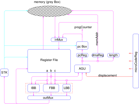
J&T is centered around the register file, whose structure is the same as the one used in APEmille. Data are transferred from memory to register file (and back) through a bi-directional port. Data available on the register file can be operated upon in just a few ways:
-
•
Data words can be fed to the mathematical processor (the set of three units within the red dashed frame). The latter contains a floating-point data-path (Floating-point Building Block, FBB), an integer arithmetic unit (Integer Building Block, IBB) and a further unit providing first approximations of some useful mathematical functions, such as . This block is known as a Look-Up-Table Building Block (LBB) in APE jargon. Results of the mathematical block are written back to the register file (for later reuse or store onto the memory).
-
•
Data can be moved to the Address Generation Unit (AGU), where a memory address or a branch-address can be computed out of two register-operands and one immediate-operand (the displacement). New (data or branch) addresses are stored in appropriate registers to be used at the next memory reference or branch.
-
•
Logical tests can be evaluated on results computed from the mathematical processor. The outcome of such tests goes onto a stack where more complex logical conditions can be evaluated. The top of the stack is used to control program flow by acting on the program-counter circuitry (corresponding to if (...) then in high level programs) or to block write operations onto memory or register file (where (...) statements in APE-like high level programs).
The processor is controlled by a relatively large program word (called the Micro-code Word) directly controlling the various devices in the node. (Almost) no instruction decoding is performed on chip. This scheme has been successfully used in the node processors of both APE100 and APEmille. A word size of 128 bits is large enough to control the system.
In the following, we describe in more details several key units of the processor.
8.1 The memory Interface and the Network Interface
In this section we describe the memory and network interface, sketched as memory grey box in figure 3. A basic structure of this subsystem is shown in fig 4.
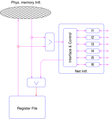
The diagram shows several paths:
-
•
there is a direct data path from the Register File to the physical memory interface (and vice versa), supporting normal memory access.
-
•
Data from memory can be also fed to the Network Interface (and eventually routed to a remote node). Conversely, data arriving from the Network (from a remote node) can be routed to the Register File.
-
•
Data words may be sent to the network from the register file. This is a novel feature, allowing register-to-register remote communications. This feature reduces remote bandwidth requests in some cases (notably in the evaluation of the Dirac operator).
-
•
The network interface receives data from the memory (or the registers) and route it to the appropriate destination through one of the six links (Details on the network itself will be provided later on).
In figure 5 we show a more detailed view of the interface to the physical memory.
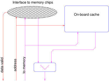
We see that memory is divided into cache memory and external memory:
-
•
external memory. External memory implements the large memory bank of the node. As discussed in the section on technologies, we may use (for instance) DDR 1 Gbit memory chips. We have several options of memory bus width and bank size satisfying bandwidth constraints (see table 7). We want to leave these options open at this point in time. For this reason, figure 5 still has a grey box. This grey box contains the actual state machine controlling memory access, memory correction circuitry, refresh control circuitry and any other ancillary logic. The box will be designed in detail at a later stage of the project, after the actual memory technology has been selected. For the moment, we model the block by a simple interface in which data words coming from the memory are validated by an ad-hoc signal.
-
•
cache memory A limited amount of on chip memory is needed in the node. Fast access on-chip memory will be used to store control variables (i.e. loop counters) and memory pointers. These variables were stored in the data memory block of the control processor (T1000) in APEmille. Indeed, these variables have very irregular access patterns and very short access bursts. The use of relatively long-latency dynamic memory would adversely impact performance. On-chip memory does not need to be very large, of the order of 1K data words. Note that, in spite of the name, this is not a true hardware controlled cache system, since the decision to store variables on-board or otherwise is statically made at compile time (one very simple strategy would be to store on-board all non vector integer quantities defined by a program).
In any case, as seen by the processor, the memory interface has a word-width of 128 bits (one complex double precision number) and provides one new word at each clock cycle in burst mode. Addressing is done on 64-bit boundaries (so real and integer variables can be stored efficiently).
8.2 The Instruction Cache
Actual LQCD simulations typically spend an extremely large fraction of the running time in just a few critical loops. For instance, a full-fermion hybrid Monte Carlo code spends nearly 95% of the time in the kernel used to compute the value of the Dirac operator on the fermion fields. Under these conditions, an instruction-cache system should have very large efficiency. We may exploit this feature by storing node programs in the same memory bank as data, with obvious advantages in terms of pin-count, real-estate reduction and cost savings.
We consider a control word (micro-code word) of 128 bits, equal to the word size that can be fetched from memory at each clock cycle. We may modify the memory interface as shown in fig 6.
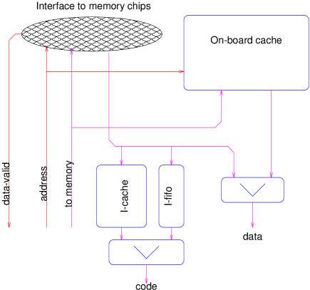
Consider for the moment just the instruction FIFO. The memory controller (not shown in the picture) continuously looks-ahead and prefetches instructions from the memory, at all machine cycles in which data-memory transactions are not in progress. Under the fully pessimistic assumption that all program cycles involve data-memory accesses, this mechanism reduces performance by a factor . Now consider the instruction cache. The instruction cache is loaded when or before the critical kernels are executed the first time (possibly under program control: the program writer may advise the compiler through appropriate directives that some routine or do loop is a critical kernel). The program then completes all following loops fetching instructions from the cache without incurring in any time penalty. The expected efficiency is
| (3) |
where is the fraction of cached program instructions. If we expect to cache 90% of all used instructions (a rather pessimistic value) we may still expect 90% program efficiency.
The size of the cache needed to accommodate the computational kernels is an important parameter. We have analyzed several LQCD kernels used in TAO and TAOmille physics programs and we have found that a cache size of the order of 16 kWords is large enough.
8.3 The Register File
The register file has the same architecture as in APEmille. The register file has three read-only ports, one write-only port and one bi-directional port. The read-only ports are used to feed data to the mathematical processor, while the write-only port stores data from the mathematical processor onto the RF. The bi-directional port is used for memory access. All ports can be used at each clock cycle (five independent addresses are needed).
The word size of the processor is 64 bits, and complex numbers are stored as pair of (adjacent) registers.
The depth of the register file affects the performance of the node. If there are not enough registers available, temporary results cannot be hold on-register. Memory bandwidth requirements increase and program efficiency decreases. In APEmille, 512 registers (or 256 register pairs) were used. Table LABEL:tab:codelength lists the number of registers used by critical LQCD kernels programmed in TAO and compiled for APEmille. As we see, less than 256 are needed in all programs. We plan to design a register file of the same size as APEmille (512 lines). If we find out that such a large system does not work at the required speed, we know that the size can be halved without serious problems.
8.4 The Mathematical Processor
The computing engine contained in J&T performs three tasks:
-
1.
it performs the floating-point (FP) (and, less frequently, integer) arithmetic operations heavily used in any scientific code. This is of course the most important functionality of the computing engine. All design trade-offs must be guided by the aim of achieving highest possible sustained performance for the most relevant tasks. As already discussed, we will use the IEEE double precision format only. The system will be heavily optimized for the arithmetics of complex-valued numbers.
-
2.
it computes first approximations of several important special functions (as already remarked, these functionalities are called LUT operations in APE jargon).
-
3.
it performs all (mostly integer) arithmetic and logic operations needed to compute memory addresses. This task was carried out in a separate chip in APEmille, with dedicated hardware. We plan to share just one processor for this task and the previous one (and also for the fourth task, described below). As shown elsewhere, the price paid by this optimization in terms of performance is small.
-
4.
it performs all arithmetic and logic operations supporting the evaluation of branch conditions. All considerations made before about addressing also apply here.
We plan, for obvious reasons, to reuse to a large extent the logical design and implementation of the arithmetic block used in APEmille (called FILU for Floating - Integer - Logic Unit). This goal is most easily reached by extracting from FILU the double precision FP data path, the integer data path and the LUT circuitry, and building more complex operators as combinations of these building blocks. We recall that the FP data path performs the normal FP operation () and conversions between FP and integer numbers, while the integer data path performs standard arithmetic and logic operations in integer format. We call these basic data paths the FBB (Floating Building Block), the IBB (Integer building Block) and the LBB (LUT Building Block).
Experience with the development of APEmille has taught us that a minor effort is needed to finalize the design of the IBB and LBB. Here we consider in details only the FBB. The architecture that we consider is shown in figure 7. It uses data stored in the RF, that contains 256 register pairs. The two elements of the pair share the same address on each of the three ports. A complex operand has its real and imaginary parts stored on the same word of both registers, while a real operand sits on any location of either block. A vector operand finally is made up of two independent real values, stored in the same way as a complex operand. Vector operations can be efficiently used in LQCD codes for the generation of random numbers.
The FBB (see figure 7) uses four basic floating point blocks, wired in such a way as to:
-
•
compute the complex-valued version of the normal operation:
(4) (5) -
•
compute one real-valued normal operation on operands coming from any element of any register.
-
•
compute two real-valued normal operations on ordered operand pairs sitting on the right and left register banks respectively (vector mode).
Some basic figures of this architecture are collected in table 13. Control of the processor requires 5 opcode bits in the microcode word and 4 addresses for the RF ports. In total control bits are needed.
| type | performance | operands in RF |
|---|---|---|
| complex | 1600 MFlops | 256 |
| real | 400 MFlops | 512 |
| real vect. | 800 MFlops | 256 |
| integer | 200 Mips | 512 |
| int. vect. | 400 Mips | 256 |
8.5 Performance Estimates
We have worked out some preliminary (but for the considered processor models rather accurate) forecasts of the expected efficiency of the processor outlined in the previous sub-sections on a few computationally intensive kernels. Our results are shown in table 14 for two versions of the kernel of the Dirac operator and for the main kernel of the Lattice Boltzmann Equation (LBE) solver.
| Kernel | normals | APEmille | apeNEXT |
|---|---|---|---|
| Dirac1 | 336 | 44% | 45% |
| Dirac2 | 336 | 58% | 72% |
| LBE | 870 | 55% | 60% |
The first two codes are appropriate for LQCD programs, while the last kernel has been used for the simulation of turbulent fluid flows on APE systems. The two Dirac kernels refer to a simple program written in TAO (Dirac1) and to an highly optimized code written in assembly (Dirac2). We can safely conclude that the performance will be in most cases comparable or superior to APEmille.
We are still working to make our prediction more accurate and to test the efficiency of the processor on a larger set of computational kernels.
8.6 Implementation Issues
In table 15 we estimate the gate count of the largest logical blocks used in J&T. In the table we foresee a CMOS technology, as discussed in a previous section. Most values are evaluated by using appropriately scaled corresponding figures for APEmille and allowing large safety margins.
| what | APEmille | scale Factor | apeNEXT (gates) | apeNEXT() |
|---|---|---|---|---|
| Reg File | 200 K | 2 | 400K | 5.0 |
| Math. Unit | 100 K | 2.5 | 250K | 3.7 |
| Intf. | 30 K | 2 | 60K | 1.0 |
| Data cache | 0 | NA | 4.4 | |
| Instr. cache | 0 | NA | 34 | |
| Total | 330 K | 4.5 + cache | 700K + caches | 48 |
Power dissipation for this system is less than 2.5 W at 200 MHz (assuming that about 30% of the gates switch at each clock cycle). This processor fits into a reasonably small die and has a relatively small pin count.
9 The Interconnection Network
The interconnection network is specifically tailored to the needs of LQCD simulations. The networks supports rigid data transfers between:
-
•
nearest neighbour nodes in the positive and negative direction of the three axis (single hops)
-
•
next to nearest nodes, whose node-coordinate differ by 1 in two of the three dimensions (double hops)
More formally, the network performs rigid shifts of the mesh of processors onto itself:
| (6) |
where labels the coordinates of each processor. The shifts , with and , are the same for each processor.
Each link has a target bandwidth of at least 300 MBytes/sec per link. Each node needs six links to support all the above described communication patterns.
From the point of view of system architecture the network is logically synchronous and supports SIMD program flows, although at the layer of the physical link, no (wall-clock) time synchronization is needed.
This definition can be made more precise in the following way:
-
•
Consider a SIMD program started on all nodes of the machine. Each node, while executing the program, starts a well defined sequence of remote communications. The sequence is the same for all nodes.
-
•
we tag all remote communications by the following set of attributes:
(7) where the ’s were defined before, is the size of the data packet associated to the communication and is an identifier that labels all communications issued by each program (in the following, we call the message-tag). is initialized at 0, when starting the program and is incremented every time a new communication is started. In other words, defines an ordering of all communications inside the program. Note that all attributes of each remote communication are equal on all nodes.
-
•
The network interface of each node accepts data bound to a remote node and tries to send it to destination. Note that although all nodes necessarily send the same sequence of packets, the (wall-clock) time at which a new data transfer starts may differ slightly among nodes. The following simple protocol controls the ensuing traffic:
-
1.
Each network interface refuses to accept a data packet coming from a different node and tagged by unless it has been already instructed by its own node to start transferring .
-
2.
Each network interface delivers incoming data in strict ascending order.
This protocol is needed to make sure that all messages reach destination in the appropriate ordering. As we see, very simple rules are needed to reach this goal under the assumption that programs follow the SIMD paradigm.
-
1.
Note that the network can perform several useful sanity checks:
-
•
Once a node instructs the network to send a data-packet to a given destination, the network implicitly knows which packets it should expect on its links with a given tag. For instance, if a data-packet must be routed to south - east, then data with the same tag is expected from west for delivery at the local node and from north to be routed to east. The network interface can check that this is actually the case.
-
•
The network can also check whether the right sequence of tags is received within a (programmable) time-out delay.
-
•
The network can further check whether the data-sizes of all messages associated to a given tag are equal.
All these checks are important to help debug either ill-functioning hardware or wrong programs.
Error rates in the network are an important issue. In plain fact, we do not know the Bit Error Rate (BERR) that we may expected on fast links. We are only able to quote the upper limit on the BERR implied by the safe operation of the APEmille prototype (). The BERR value needed for an error free apeNEXT operation on runs lasting a few days is an embarrassingly low . For this reason, we have decided to stay on the safe side and to design a network partially able to recover from errors. If we are able to recover from errors, a much more manageable picture emerges: for instance a more modest BERR implies the failure of one transmission burst every second on the entire machine.
We are considering a retry mechanism, shown in figure 9 that has only a moderate impact on communication latency:
-
•
We divide each data block traveling on a remote link in relatively short bursts (say, 16 bytes) followed by a cyclic-redundancy-check (CRC).
-
•
Data bursts are sent from the transmitting nodes, followed by their CRC. A small number of bursts is kept on the transmitting node, stored inside a FIFO queue, also after transmission.
-
•
The receiving end of the link checks the CRC of each burst as it arrives. If the check is successful it delivers received data. The latency implied by this procedure is not longer than the size of each burst.
-
•
If an error is detected, the receiving end requests the corrupted burst to be retransmitted. This is possible, since relevant data is still available on the transmitting side of the link.
We plan to finalize most of the high level details of the network using a black box model of the physical link layer. In this way we can complete most of the design even before selecting the actual link technology. In parallel, we are already carrying out tests on some of the link technologies.
10 Machine Assembly and Partitioning
We plan to assemble a certain number of APEmille processors on a printed circuit board (PCB). Preliminary evaluations suggest that 16 processors can be placed on one PCB, of roughly the same size as the one used for APEmille. For comparison, note that one APEmille PCB houses 8 processors. In this case however a large (almost 50%) fraction of the real estate is used by the control processor and ancillary circuitry. If we use PCB’s of the same size as APEmille, we can immediately reuse the mechanical components of the older system.
At this point in time we have two options for the topology of the nodes belonging to one PCB. The first option is a three-dimensional structure with processors. The second option implies a two-dimensional set-up of processors. PCB’s are assembled inside a crate. All PCB’s inside one crate are connected to a communication backplane. If we use the mechanical components developed for APEmille, we can reasonably house up to 16 PCB’s inside one crate. Larger machines use more crates.
If we use the first option for the node topology inside a PCB, we can allocate onto the backplane all links in two of the three dimensions (say, directions y and z), building a system of size . Communications in the x direction are implemented via cable links. If we assemble and connect together crates, we obtain apeNEXT systems of size . This option is very similar to the one used by APEmille, where systems of size are allowed. We call this arrangement Option 1A.
It is possible to use the same structure of the PCB as above, wiring however the unit inside a crate according to a topology. In this case large machines contain nodes. This is option 1B.
In the case that the second option for the PCB is selected, we allocate all links belonging to one of the spatial directions (say, direction z) onto the backplane. Links in the x and y directions stemming out of the PCB use cable links instead. Using this arrangement, systems of size can be assembled. This is option 2. Some basic figures relevant to both options are collected in table 16.
| Option 1A | Option 1B | Option 2 | |
|---|---|---|---|
| number of procs. | 16 | 16 | 16 |
| Peak PCB perf. | 25.6 GFlops | 25.6 GFlops | 25.6 GFlops |
| topology | |||
| crate topology | |||
| Large-systems | |||
| Remote links (PCB) | 40 | 40 | 48 |
| Remote links (BP) | 32 | 24 | 32 |
| Remote links (cables) | 8 | 16 | 16 |
In both cases, a large number of signal must be routed on the backplane. This is a serious but not formidable engineering problem. Assuming that 20 data lines are needed per link, we have 640 pins carrying data from the PCB to the backplane (see again table 16). This requires as little as about 17 cm on the PCB edge, using high-density high-speed matched-impedance connectors developed by several vendors (see for instance [19]). Of course, special care must be taken in the design of accurately matched transmission lines, both on the backplane and on the main PCB.
As discussed earlier, the backplane must also house a CPCI backplane. This is made by a straightforward copy the well tested CPCI backplane developed for APEmille.
We will decide later on in the design phase on the selected topology, using information from test setups and taking also into consideration the relative merits of the two solutions from the point of view of physics simulations.
11 Software: The Programming Environment
The apeNEXT programming environment will be initially based on two main lines:
-
•
The TAO programming language, extensively used in APE100 and in APEmille, will be supported. This is necessary to allow easy and early migration of the large set of existing QCD programs on the new machine This large portfolio of programs is also going to be extremely useful for test and debugging purposes.
We do not plan to make any substantial improvement to TAO. We will just modify the back-end section of the TAO compiler, so it produces apeNEXT assembly codes.
-
•
We plan to develop a C/C++ language compiler for apeNEXT since the early phases of the project. Very few extensions will be added to the standard C syntax, with the goal of minimizing the effort for the programmer in learning a new language. SPMD parallelism will be realized by just a few special constructs, similar to the ones already present in TAO:
-
1.
the where statement executes code blocks based on local conditions.
-
2.
the all, none, any keywords in a standard C condition perform aggregate evaluation of local conditions.
-
3.
Remote communications will be specified by constant pointers.
The compiler will be implemented by porting already available public domain compilers (like, for instance, the GNU C/C++ compiler or lcc) with the needed SPMD extensions in the front-end (the language definition) and all necessary changes in the back-end, to produce the target assembly. A similar GNU-gcc based compiler prototype for APEmille [20] is currently evaluated.
Note that, by using already available compilers, it will be relatively easy to implement all SPMD extensions of the language on more traditional machines (like PC clusters). Conversely, already developed parallel programs written in C (and following the SIMD/SPMD paradigm) will be easily ported onto apeNEXT. We regard this possibility as our main path to build a common programming environment between apeNEXT and more traditional systems.
-
1.
We want to push still further the goal of a more general apeNEXT programming environment. We plan to merge to some extent the programming environments based on Tao and on C/C++, and at the same time enhance the portability of programs between APE systems and more traditional computer clusters. We plan to work according to the lines described in figure 10, that uses for definiteness the structure of the GNU compiler.
The blue boxes in figure 10 sketchily describe the overall organization of a modern compiler. There is a front-end block with a configurable parser that transforms the user code into an internal representation, based on a tree representation of the code and symbol tables. The back-end block maps the internal representation onto assembly code for a specific target architecture.
The APE C compiler can be implemented on the basis of existing and configurable front-ends with minor modifications to include the required syntax extensions for parallel processing. The back-end section must of course be customized to produce apeNEXT assembly code.
It is also possible to add an additional parser at the front-end level. (For instance, Fortran is implemented in this way in the GNU compilers.) We intend to follow this path and to include the TAO parser, suitably modified to generate the GNU internal representation. Indeed, TAO cannot be easily handled by standard configurable parsers because of its dynamic grammar. In figure 10 the APE specific extensions are drawn in red.
When the program outlined above is accomplished, we will have a very neat portable environment in which:
-
•
all powerful optimization techniques of a standard compiler core are available.
-
•
TAO and C codes can be compiled for a standard computer system (e.g. a PC).
-
•
C and TAO codes can be compiled for an APE system.
The design and implementation of this open programming environment is a long term and very high priority goal of our project. This is not going to be an easy task and can certainly not be finalized in short terms. Physics exploitation of apeNEXT in the early phases does not depend on this environment, since the traditional APE software tools can be used.
At the machine level, we will port to the new architecture and improve the well-established VLIW code-scheduling and code-compressing tools already used in APEmille.
12 Software: The Operating System
We plan to shape the apeNEXT operating system as a direct evolution of the APEmille system: the basic idea is that we use as much as possible the services provided by Linux on the network of host PC’s.
-
•
The apeNEXT operating system must load executable codes on the array of processing nodes and start execution of the whole system. We remind that all steps of program compilation and optimization are not done on the apeNEXT processors itself but are performed on the host PC’s (or on any other Linux machine).
-
•
The second task performed by the operating system is the support for input-output operations requested by the executing program. Note here that these operations use the standard file systems available on the host PC’s (or, on any networked disk server). Of course, large data transfers, where high bandwidth is needed, are performed in parallel by all PC’s on local disks. Later on, we will make some additional remarks on this point.
-
•
The third task performed by the operating system is the monitoring and control of all nodes at a low level. Typical examples include the inspection and setting of status-registers, the analysis of error conditions, explicit writes or reads to memory locations.
All functions described above are handled by the APEmille operating system in a reasonably efficient and user-friendly way. Most operations can be easily moved onto apeNEXT by rewriting only the lowest layer levels of the operating system, like device drivers or the functions mapping a specific operation on a specific node onto the appropriate PC. We expect therefore to be able to put to work quickly an early version of the system.
An area where we would like to come up with new ideas, not needed however for the early commissioning of apeNEXT, is some version of a parallel file system, where large field and propagator configurations can be stored in a standard format. This is an obvious starting point to allow the sharing of QCD configurations among collaborating groups. We see this work as a partial contribution of apeNEXT to the GRID project. Work on this line will be therefore coordinated with GRID.
13 Design Method
In designing the needed VLSI components as well as the overall system, we want to follow the method used in APE100 and APE1000, with a number of improvements to make it more efficient and faster. The main advantage of this method has been shown in APE100 and APEmille: in both cases all components of the machine were designed ”first-time-right”.
The main idea behind our method is some informal implementation of ”hardware-software co-design” techniques:
-
•
We base our design on a VHDL model of a large and significant fraction of the whole system. The model contains all in-house developed systems as well as all off-the-shelf components. Initially, the model will be a very crude approximation to the actual system, gradually incorporating all details. This reference model is available at all collaboration sites.
-
•
All VLSI (or FPGA based) components of the system are derived with high quality synthesis tools from the VHDL design. In the (hopefully rare) cases where some components cannot be synthesized from a VHDL description, a VHDL model is built anyway, and test vectors for the actual implementation are derived by the VHDL model. Non-VLSI parts of the systems (i.e., processing boards) will be modelled in VHDL by their designers.
-
•
The VHDL model supports a reasonable approximation of the interaction with the host system (operating system).
-
•
All software developments are immediately tested on the VHDL model. At an early stage of the design, tests will involve performance estimates on crudely modelled architectural choices. As the level of details of the model increases, actual programs, in all their intricacies, will be executed on the model, giving quick feed-back on any design detail.
As an improvement with respect to APEmille, we will insist on:
-
•
a continuous availability of the model at all collaboration sites, so all members of the collaboration can easily monitor the effects of a design change made elsewhere. This can be achieved with reasonable effort by keeping a master copy of the model on an AFS cell available from all sites.
-
•
an effort to allow access to the model from a basic version of the operating system, so that even the more physics-oriented members of the collaboration can exercise it.
-
•
a systematic use of blind-test procedures: at all stages of the design phase, test sequences for any part of the machine will be prepared and executed by someone who has not been directly involved in the design.
Finally, we address the issue of the design of some VLSI blocks that depend critically on some element which is either not under our direct control or not completely defined at this stage. Examples of this situation are the details of the memory system (which heavily depends on the type of memory available at the time when the prototypes are built) for the custom processor, or the actual choice for the physical layer of the interconnection links. Changes made in memory technology during the design lifetime of APEmille have indeed adversely affected that project, as large subsystems within J1000 and T1000 processors had to be modified to adapt to changing memory specifications.
We want to solve this problem by confining all details of the memory and link interfaces in a ”grey box”, that interacts with the rest of the design with some simple and rather general data and control paths. In this way, a very large fraction of the design can be finalized independently, while the interface-specific blocks will be procured (if available from external sources) or designed in detail at the last moment.
14 Conclusions
This document has described physics requirements and the basic architecture of a next generation LQCD computer project. We think that the well-tested SIMD/SPMD architecture of the previous APE generations is still the best choice for a LQCD-focused high performance engine. At the engineering level, we plan to use technologies similar to those used in APEmille. We think that this choice reduces development costs and risks.
In the near future, collaboration between groups active in LQCD simulations will become tighter and tighter. For this reason we plan to work hard on the development of a software environment allowing easy migration between apeNEXT and more traditional computers.
Acknowledgments
Several people have helped shape the basic ideas of apeNEXT and contributed several important pieces of information. We would like to thank I. D’ Auria, W. Friebel, J. Heitger, M. Loukyanov, S. Menschikov, A. Sapojnikov, T. Sapojnikova, L. Schur, A. Thimm. N. Christ, N. Eicker, Y. Iwasaki, T. Lippert and K. Schilling have provided valuable information on the status and perspectives of their projects.
References
- [1] for a recent review, see: N. Christ, “Proceedings of Lattice99”, Nucl. Phys. B (Proc. Suppl.), in press.
- [2] R. Tripiccione “APEmille”, Parallel Computing 25 (1999) 1297.
- [3] F. Jegerlehner et al., “Requirements For High Performance Computing for Lattice QCD: Report of the ECFA Working Panel”, Preprint ECFA/99/200.
- [4] F. Aglietti et al., “Proposal for a Multi-Tflops Computing Project”, Rome Preprint 1255/99.
- [5] See for example: P. de Forcrand, Nucl. Phys. B (Proc.Suppl.) 47 (1996) 228; A. Frommer, Nucl. Phys. B (Proc.Suppl.) 53 (1997) 120; K. Jansen, Nucl. Phys. B (Proc.Suppl.) 53 (1997) 127, and references therein.
- [6] TAO Reference Manual, (E. Panizzi and V. Ghisalberti Eds.), 1994.
- [7] R. G. Edwards, I. Horvath and A. D. Kennedy, Nucl. Phys. B484 (1997) 375; B. Bunk, S. Elser, R. Frezzotti and K. Jansen, Comput.Phys.Comm. 118 (1999) 95, hep-lat/9805026; K. Jansen and C. Liu, Nucl. Phys. B (Proc.Suppl.) 53 (1997) 974; C. Liu, A. Jaster and K. Jansen, Nucl.Phys. B524 (1998) 603; K. Jansen and C. Liu, Nucl.Phys. B453 (1995) 375.
-
[8]
http://nicewww.cern.ch/ les/grid/welcome.html and
http://www.infn.it/grid/ - [9] S. Aoki et al., HEP-LAT/9903001.
- [10] See, e.g., C.T. Sachrajda, summary talk at Lattice 99 (Pisa), hep-lat/9911016 and references herein.
- [11] Y. Iwasaki, private communication. Also CP-PACS Collaboration, Internal report, 1999.6.20, to be published.
- [12] N. H. Christ, private communication.
- [13] N. Eicker and T. Lippert, private communication.
- [14] The Lattice Hadron Physics Collaboration, ftp://www-ctp.mit.edu/pub/negele/LatProp/LatticePropFinal.ps.
- [15] F. Csikor et al., hep-lat/9912059
- [16] H. Simma, “PC’s for Multi_TFlops LQCD Compute Engines?”, Proceedings of the Workshop PC-NETS, INFN/TC-99/09.
- [17] AMD Athlon Processor Data Sheet (Publication 21016), March 2000.
- [18] See, for instance, http://www.transmeta.com/crusoe
- [19] See, for instance, http://www.teradyne.com/prods/bps/vhdm/intro.html
- [20] http://apemaia.roma1.infn.it/betto/C++_apeNEXT.html