High Resolution Hybrid Pixel Sensors for the
TESLA Linear Collider Vertex Tracker
Abstract
In order to fully exploit the physics potential of a future high energy linear collider, a Vertex Tracker, providing high resolution track reconstruction, is required. Hybrid Silicon pixel sensors are an attractive option, for the sensor technology, due to their read-out speed and radiation hardness, favoured in the high rate environment of the TESLA linear collider design, but have been so far limited by the achievable single point space resolution. In this paper, a conceptual design of the TESLA Vertex Tracker, based on a novel layout of hybrid pixel sensors with interleaved cells to improve their spatial resolution, is presented.
keywords:
pixel; vertex detector; linear collider1 The requirements of the linear collider physics programme
The next generation of high energy experiments, following the LEP and SLC programs, will be at a linear collider, operating at centre-of-mass energies ranging from the pole up to about 1 TeV. Expected to be commissioned by the end of the first decade of the new millennium, the linear collider will complement the physics reach of the Tevatron and LHC hadron colliders in the study of the mechanism of electro-weak symmetry breaking and in the search for new physics beyond the Standard Model. Both precision measurements and particle searches set stringent requirements on the efficiency and purity of the flavour identification of hadronic jets since final states including short-lived and -quarks and leptons are expected to be the main signatures. High accuracy in the reconstruction of the charged particle trajectories close to their production point is required in order to reconstruct the topologies of the secondary vertices in the decay chain of short-lived heavy flavour particles.
If a Higgs boson exists with mass below 150 GeV/c2, as indicated by the fit to the present electro-weak data Gross , it will be essential to carry out precision measurements of its couplings to different fermion species as a proof of the mass generation mechanism and to identify its Standard Model or Supersymmetric nature higgs1 . This can be achieved by accurate determinations of its decay rate to , , , and gluon pairs to detect possible deviations from the Standard Model predictions higgs2 . Since the rates for the Higgs decay modes into lighter fermions , or into gluon pairs are expected to be only about 10% or less of that for the dominant process, the extraction and measurement of the signals of these decay modes requires suppression of the contribution by a factor of twenty or better while preserving a good efficiency.
The measurement of the top Yukawa coupling TopYuk as well as the top-quark mass measurement will require efficient -tagging to reduce combinatorial background in the reconstruction of the six and eight jet final states. If Supersymmetry is realized in nature, the study of its rich Higgs sector will also require an efficient identification of -jets and leptons to isolate the signals for the decays of the heavier , and bosons from the severe combinatorial backgrounds in the complex multi-jet hadronic final states. Due to the expected large -jet multiplicity, highly efficient tagging is required to preserve a sizeable statistics of the signal events. Finally, both and -tagging will be important in the study of the quark scalar partners, while identification may be instrumental in isolating signals from Gauge Mediated Supersymmetry Breaking GMSB .
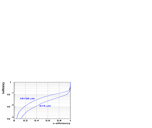
A set of curves representative of the performance of a jet flavour tagging algorithm at the linear collider are given in Figure 1 under two different assumptions for the track impact parameter resolution. The requirement of efficient identification with a rejection factor against -jets of more than ten, highlights the need of track impact parameter resolution better than in both projections. It is important to minimise the multiple scattering contribution to the impact parameter resolution. In fact, / discrimination is obtained mostly by probing the difference in charged decay multiplicities and invariant masses of the and hadrons. This requires to identify the majority of charged decay products that have typical momenta of a few GeV/c in multi-jet events. A precise determination of the track perigee parameters close to their production point also assists in the track reconstruction and improves the momentum resolution. The addition of the Vertex Tracker space points with 7 m resolution to those from a TPC main tracker improves the estimated momentum resolution from 1.5 10-4 (GeV/c)-1 to 0.6 10-4 (GeV/c)-1 for charged particles of large momentum. The design of the linear collider Vertex Tracker and the choice of the sensor technology are driven by these requirements, to be achieved within the constraints set by the accelerator induced backgrounds at the interaction region and by the characteristics of the physics events.
In the next section these constraints are discussed with specific reference to the TESLA linear collider project, while section 3 presents the conceptual design proposed for the Vertex Tracker. The silicon pixel sensor technology, developed to overcome the hybrid pixel sensor limitations in terms of single point space resolution, is discussed in details in section 4.
2 The experimental conditions at the TESLA interaction region
Several concepts have been developed for the acceleration, preservation of low emittance and final focusing of electron and positron beams at energies in excess of 200 GeV/beam lcreview . The TESLA project CDR has proposed to use superconducting accelerating structures, operating at L-band frequency that delivers very long beam pulses ( 900 s) accelerating up to 4500 bunches per pulse. This scheme allows a large bunch spacing (190-340 ns) making it possible to resolve single bunch crossings (BX) and also to perform fast bunch-to-bunch feedback needed to stabilize the beam trajectory within a single pulse, thus preserving the nominal luminosity of 3-5 cm-2 s-1. The large luminosity of each individual bunch-crossing ( 2.2 nb-1 BX-1) and the large number of bunches in a single pulse imply a high rate of background events that need to be minimised by identifying the bunch corresponding to the physics event of interest.
A primary source of background at the linear collider interaction region is the incoherent pair production in the electromagnetic interactions of the colliding beams. These particles are confined by the solenoidal magnetic field, spiralling in an envelope defined by the field strength, , and their intrinsic transverse momentum acquired at production and the subsequent deflection in the electric field of the opposite beam. The pairs represent an irreducible source of spurious particle hits, which interferes with the reconstruction of the particles from the physics processes of interest. The maximum radius and longitudinal position of crossing of the envelope of deflected pairs defines both the inward bound for the first sensor layer and its maximum length. At 1.2 cm radial distance from the TESLA colliding beams, with a magnetic field = 3 T, the hit pair density is expected to be 0.2 hit mm-2 BX-1 with cm available in the longitudinal coordinate to fit the first sensitive layer of the detector. An additional background source that needs to be taken into account in the choice of the sensor technology is the flux of neutrons photo-produced at the dump of electrons from pairs and radiative Bhabha scattering and of beamstrahlung photons. The computation of this neutron flux at the interaction region relies on the modelling of their production and transport in the accelerator tunnel and in the detector and is subject to significant uncertainties. Estimated fluxes are of the order of a few 109 (1 MeV) cm-2 year-1 Tesch ; Ye , where the anticipated neutron flux has been normalised in terms of equivalent 1 MeV neutrons assuming NIEL scaling. Finally the large cross-section requires single bunch identification and high resolution on the longitudinal position of production of forward charged particles in order to suppress to a few % the rate of two photon background overlap with physics events.
In addition to these background sources, the occupancy from the charged particles inside dense jets in multi-parton hadronic final states has to be considered. A study of and events at = 500 GeV showed that at 3.0 cm from the interaction point, about 20 % (10 %) of the particles in the jet have at least one additional hit from another particle of the same jet within a 150 distance in the () plane, which corresponds to the typical two-track separation capability of a microstrip detector. Therefore, sensors with small sensitive cells have to be used in order to avoid a large number of merged hits and ambiguities in the pattern recognition.
In summary, the linear collider Vertex Tracker must be able to provide a track impact parameter resolution better than in both the and projections for jet flavour identification, identify single bunch crossings separated by about 200 ns to reduce pair and backgrounds and have sensitive cells of 150 150 m2 or less to keep the occupancy from pairs and hadronic jets below 1%. There are two types of such silicon sensors, already used at collider experiments, that have the potential to satisfy these specifications in terms of sensitive cell size: the Charged Coupled Devices (CCD) and hybrid pixels sensors. The CCD sensors have successfully been used for the SLD Vertex Detector at the SLC collider at SLAC vxd3 while hybrid pixel sensors, pioneered by the WA-97 experiment at CERN WA97 , have been adopted at LEP in the upgraded DELPHI Silicon Tracker SiTracker . These have been further developed for the ALICE alice , ATLAS atlas and CMS cms experiments to meet the experimental conditions of the LHC collider. CCD detectors have been already proposed for the linear collider Vertex Tracker ccdlc . While CCD’s have ideal characteristics in terms of spatial resolution and detector thickness, they presently lack the required read-out speed necessary to cope with the TESLA bunch timing and are possibly sensitive to neutron damage at fluxes of the order of that expected at the linear collider. An intense R&D program is presently underway to overcome these limitations CCDnew . The use of hybrid pixel sensors for the linear collider Vertex Tracker was also proposed a few years ago and a first conceptual design of the detector was defined ABC . Compared to the CCD’s, hybrid pixel sensors have the advantage of allowing fast time stamping and sparse data scan read-out, thereby reducing the occupancies due to backgrounds, and of being tolerant to neutron fluxes well beyond those expected at the linear collider. Both these characteristics have been demonstrated for their application in the LHC experiments. On the other hand, there are areas of R&D that are specific to the linear collider, namely the improvement of the pixel sensor spatial resolution and the reduction of its total thickness.
3 The TESLA Vertex Detector design
The proposed layout of the TESLA Vertex Detector ABC based on hybrid pixel sensors is shown in fig. 2 and consists of a three-layer cylindrical detector surrounding the beam-pipe complemented by forward crowns and disks extending the polar acceptance to small angles. This geometry follows solutions adopted for the DELPHI Silicon Tracker.
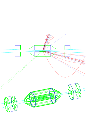
The first detector layer, closest to the interaction region, is located at a radius of 1.2 cm and has a length of 10 cm. The two additional barrel layers are located at 3.5 cm and 10 cm respectively and have a polar acceptance down to . At lower angles, additional space points are obtained by extending the barrel section by a forward crown and two disks of detectors providing three hits down to . The transition from the barrel cylindrical to the forward conical and planar geometries optimises the angle of incidence of the particles onto the detector modules in terms of achievable single point resolution and multiple scattering. This tracker can be assembled by two independent half-shells, allowing its installation and removal with the beam-pipe in place. Overlaps of neighbouring detector modules will provide an useful mean of veryfing the relative detector alignment using particle tracks from dedicated calibration runs taken at centre-of-mass energy. The geometry optimisation and the study of the physics performances of the Tracker design has been performed with a GEANT based simulation of the detector, accounting for benchmark physics processes with enhanced forward production cross-section, such as , pair and backgrounds, local pattern recognition and detector inefficiencies. The impact parameter resolution has been obtained by a Kalman filter track fit to the associated hits in the Vertex Tracker and in the TPC.
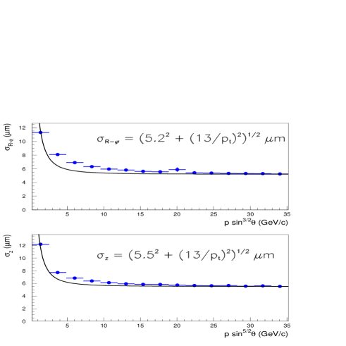
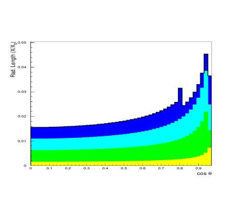
In order to achieve a resolution for the impact parameter reconstruction better than 7 m for tracks at large momenta, a detector space point accuracy of better than 10 m must be obtained. The requirement on the multiple scattering contribution to the track extrapolation resolution, lower than 30 m/, and the need to minimise the amount of material in front of the calorimeters and to ensure the optimal track matching with the main tracking system, set a constraint on the material budget of the Vertex Tracker to less than 3 % of a radiation length (). These requirements can be fulfilled by adopting 200 m thick detectors and back-thinning of the read-out chip to 50 m, corresponding to 0.3 % of a radiation length, and a light support structure. The present concept for the mechanical structure envisages the use of diamond-coated carbon fiber detector support layers acting also as heat pipes to extract the heat dissipated by the read-out electronics uniformly distributed over the whole active surface of the detector. Assuming a power dissipation of 60 W/channel, the total heat flux is 450 W, corresponding to 1500 W/m2, for a read-out pitch of 200 m. Preliminary results from a finite element analysis show that pipes circulating liquid coolant must be placed every 5 cm along the longitudinal coordinate except for the innermost layer where they can be placed only at the detector ends to minimise the amount of material. Signals will be routed along the beam pipe and the end-cap disks to the repeater electronics installed between the Vertex Tracker and the forward mask protecting the Vertex Tracker from direct and backscattered radiation from the accelerator. The material budget for the proposed design is shown in Figure 4.
4 Hybrid pixel sensors with interleaved pixels
The desired impact parameter resolution defined in section 1 requires a single point precision in the Vertex Detector better than . This can be accomplished sampling the diffusion of the charge carriers generated along the particle path and assuming an analog read-out to interpolate the signals of neighbouring cells. In such a case, the expected resolution is , where is a centroid finding constant and S/N defines the performance of the front-end electronics in terms of signal amplitude normalised to the noise. Given that the charge diffusion is in thick silicon, its efficient sampling and signal interpolation requires a pitch of not more than 25 m. This has been successfully proven to work in one-dimensional microstrip sensors Anna . In pixel devices the ultimate read-out pitch is constrained by the front-end electronics, to be integrated in a cell matching the sensor pattern. At present, the most advanced read-out electronics have a minimum cell dimension of not suitable for an efficient charge sampling. The trend of the VLSI development and recent studies Snow on intrinsic radiation hardness of deep sub-micron CMOS technology certainly allows to envisage of a sizeable reduction in the cell dimensions on a linear collider timescale but sensor designs without such basic limitations are definitely worth being explored.
A possible way out is to exploit the capacitive coupling of neighbouring pixels and to have a read-out pitch n times larger than the implant pitch Bonvicini . The proposed sensor layout is shown in Figure 5 for n=4. In this configuration, the charge carriers created underneath an interleaved pixel will induce a signal on the read-out nodes, capacitively coupled to the interleaved pixel. In a simplified model, where the sensor is reduced to a capacitive network, the ratio of the signal amplitudes on the read-out nodes at the left- and right-hand side of the interleaved pixel in both dimensions will be correlated to the particle position and the resolution is expected to be better than for an implant pitch of 25 m or smaller. The ratio between the inter-pixel capacitance and the pixel capacitance to backplane will play a crucial role, as it defines the signal amplitude reduction at the output nodes and therefore the sustainable number of interleaved pixels. Calculations with such capacitive network models Pindo show that resolutions similar to those achieved by reading out all pixels are obtainable if the signal amplitude loss to the backplane is small. Recent tests on a microstrip sensor, with 200 m read-out pitch, have achieved a resolution with three interleaved strip layout Krammer . Similar results are expected in a pixel sensor, taking into account both the lower noise because of the intrinsically smaller load capacitance and the charge sharing in two dimensions.
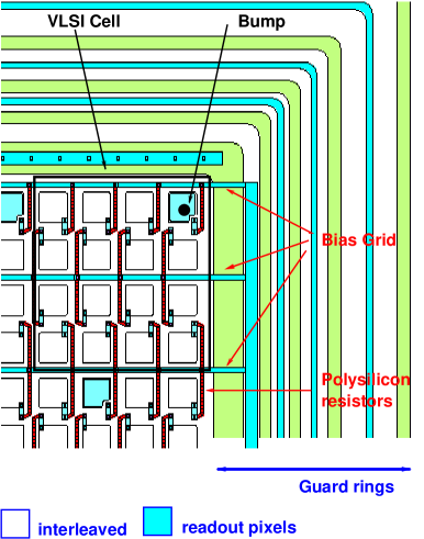
Reducing the read-out density, without compromising the achievable space resolution, is also beneficial to limit the power dissipation and the overall costs. In order to verify the feasibility of this scheme, a prototype set of sensors with interleaved pixels and different choices of implant and read-out pitch have been designed, produced and tested. These test structures have been designed in 1998 and delivered in January 1999. Ten high resistivity wafers were processed 111at the Institute of Electron Technology, Warszawa, Poland together with an equal number of low resistivity wafers for process control. A detailed description of the processing can be found in ref. AZ . A bias grid surrounding the pixel cells allows the polarisation of both the interleaved and read-out pixels and each pixel implant is connected to the metal bias line by polysilicon resistors. This is to ensure a similar potential for all pixels and hence a uniform charge collection. A metal layer is deposited on top of the pixels to be bump-bonded to a VLSI cell. The backplane has a meshed metal layer to allow the use of an infrared diode for charge collection studies. Structures with the number of interleaved pixels ranging between 0 and 3 were fitted on a 4” wafer, assuming a VLSI cell size of 200 200 or 300 300 m2. All of the structures on six undiced wafers were visually inspected and characteristic I–V and C–V curves were measured up to 250 V. The I–V and 1/C2–V curves obtained for a good structure are shown in fig. 6. Two wafers have extremely good characteristics, with a mean current of 50 nA/cm2 and about 50% of good structures. The test structures have not shown any design fault even if processing and layout optimisation has to be considered. A more detailed summary of the measurements can be found in ref. MCa . On a short term, measurements of the inter-pixel and backplane capacitances are planned, completing the electrostatics characterisation of these sensors.

A charge collection study will follow, relying on a low noise analog chip designed for microstrip sensor read-out and shining an infrared light spot on the meshed backplane. These measurements will be a proof of principle of the proposed device and define the guidelines for further iterations, aiming at a 25 m pitch.
The device thickness is a particularly relevant issue for the application of hybrid pixel sensors at the linear collider. The minimal thickness is set by the combination of the sensor noise performance and the limit of back-thinning technology for a bump-bonded assembly. Industrial standards guarantee back-thinning down to 50 m for the electronics and procedures to obtain thin sensors are currently being tested SOTT . The small load capacitance of the pixel cells should guarantee an extremely good S/N. Scaling what has been obtained for the microstrip sensors, the desired resolutions should be obtained with a 200 m thick sensor.
5 Conclusion
Hybrid pixel sensors are an attractive option for a linear collider Vertex Tracker owing to their fast read-out and radiation hardness, well suited to the high repetition rate of the TESLA design. The main present limitations of this option are the achievable single point space resolution and sensor thickness. To overcome these limitations, pixel sensor design with interleaved cells is proposed. Test structures with different configurations of interleaved cells have been designed and produced and the results of their first electrostatic characterisation are discussed. The conceptual design of a Vertex Tracker based on these detectors has been developed and its performances have been evaluated, using a detailed simulation accounting for the relevant background processes, and the preliminary results have been presented.
Acknowledgements
This activity has been funded in part by the Academy of Finland under the R&D Program for Detectors at Future Colliders and by MURST under grant 3418/C.I.
References
- (1) E. Gross, to appear in Proc. of the Int. Europhysics Conference on High Energy Physics, Tampere (Finland), July 1999.
-
(2)
H.E. Haber, in Proc. of the Int. Conf. on Physics beyond the
Standard Model, Lake Tahoe, (USA); World Scientific, Singapore, 1995;
J. Kamoshita, Y. Okada and M. Tanaka, in Proc. of the Workshop on Physics and Experiments with Linear Colliders, Morioka (Japan); World Scientific, Singapore 1996. -
(3)
M.D. Hildreth, T.L. Barklow and D.L. Burke,
Phys. Rev. Lett. 49 (1994) 3441;
M. Battaglia, to appear in Proc. of the Int. Workshop on Linear Colliders LCWS99, Sitges (Spain), May 1999 and hep-ph/9910217. - (4) A. Djouadi, J. Kalinowski and P.M. Zerwas, Zeit. Phys. C 54 (1992) 255.
- (5) G.F. Giudice and R. Rattazzi, CERN-TH 97-380.
- (6) G. Borisov, private communication.
- (7) K. Hübner, in Proc. of the 29th Int. Conf. on High Energy Physics ICHEP-98, Vancouver (Canada), July 1998, World Scientific, Singapore, 1999 and references therein.
- (8) R. Brinkmann, G. Materlik, J. Rossbach, A. Wagner (ed.), Conceptual Design of 500 GeV e-e+ Linear Collider with Integrated X-ray Laser Facility, DESY 97-048.
- (9) N. Tesch, to appear in Proc. of the Int. Workshop on Linear Colliders LCWS99, Sitges (Spain), May 1999.
- (10) M. Battaglia and S. Ye, HIP-1999-73/EXP.
- (11) K. Abe et al., Nucl. Instr. and Meth. A 400 (1997), 287.
- (12) D. Di Bari et al., Nucl. Instr. and Meth. A 395 (1997) 391.
- (13) P. Chochula et al., Nucl. Instr. and Meth. A 412 (1998) 304.
- (14) F. Antinori, in Proc. of the Int. Pixel Detector Workshop PIXEL98, FERMILAB-CONF 98-196, 41.
- (15) ATLAS collaboration, The Pixel Detector Technical Design Report, CERN-LHCC 98-13.
- (16) D. Bortoletto, in Proc. of the Int. Pixel Detector Workshop PIXEL98, FERMILAB-CONF 98-196, 22.
- (17) C.J.S. Damerell and D.J. Jackson, in Proc. of the APS Workshop on New Directions for High Energy Physics, Snowmass (USA), July 1996.
- (18) T. Greenshaw et al., to appear in Proc. of the Int. Workshop on Linear Colliders LCWS99, Sitges (Spain), May 1999.
- (19) M. Battaglia, A. Andreazza, M. Caccia and V. Telnov, in Proc. of the 2nd Workshop on Backgrounds at Machine-Detector Interface, Honolulu (USA), March 1997, World Scientific, Singapore, 1998 and in DESY 97-123E.
- (20) U. Kötz et al., Nucl. Instr. and Meth., A 235 (1985), 481.
- (21) W. Snoeys, CERN–LHCC 97-60, 139.
- (22) V. Bonvicini and M. Pindo, Nucl. Instr. and Meth. A 372 (1996) 93.
- (23) M. Pindo, Nucl. Instr. and Meth. A 378 (1996) 443.
- (24) M. Krammer and H. Pernegger, Nucl. Instr. and Meth. A 397 (1997) 232.
- (25) W. Kucewicz et al., Acta Phys. Pol. B 30 (1999) 2075.
- (26) M. Caccia et al., to appear in Proc. of the Int. Workshop on Linear Colliders LCWS99, Sitges (Spain), May 1999 and hep-ex/9910019.
- (27) T.E. Browder et al., in Proc. of the Int. Pixel Detector Workshop PIXEL98, FERMILAB-CONF 98-196, 172.