1 - An Eight Channel Time-to-Digital Converter Chip
for High Rate Experiments
Abstract
A new TDC chip has been developed for the COMPASS experiment at CERN. The resulting ASIC offers an unprecedented degree of flexibility and functionality. Its capability to handle highest hit and trigger input rates as well as its low power consumption makes it an ideal tool for future collider and fixed target experiments. First front-end boards equipped with the 1 chip have been used recently at testbeam experiments at CERN. A functional description and specification for this new TDC chip is presented.
Introduction
The COMPASS experiment at CERN was proposed to and approved by the CERN authorities to investigate the complex hadron structure. One central issue of the experimental effort will be the measurement of the contribution of gluons to the nucleon spin. Previous experiments at CERN, DESY and SLAC made decisive advances towards the understanding of the nucleon spin in terms of its quark constituents, but the role of the gluon still needs more clarification. To reach this objective a demanding state-of-the-art double-stage spectrometer with large geometrical and dynamical acceptance will be set-up and commissioned through 2000.
The low cross sections of the studied interactions which will provide insight to the physics objectives of COMPASS necessitate high beam rates. The central detector has to be capable to digest the high particle flux from the traversing beam at intensities of particles/spill. This leads consequently to the requirement of negligible dead time for the digitization units in the data acquisition system of the experiment. The anticipated amount of data on the order of several Gigabytes per spill (2.4 seconds) is at the edge of todays digitisation and bandwidth technologies.
Wherever applicable in COMPASS measurements are digitized at the detector by ‘intelligent’ front-end electronics [1]. The advantages of this scheme are obvious: besides the enormous cost savings due to obsolete data transfer and delay cables the fact of lower noise, higher bandwidth and the possibilities for data pre-processing open up new prospects for efficient data digitisation. In case of analog readout a pedestal subtraction and zero suppression is performed by the front-end devices at the COMPASS detector. To suppress background in time measurement components only those hits are read out which are time correlated to the trigger time. The distributed readout architecture of the COMPASS experiment is summarized in Figure 1.
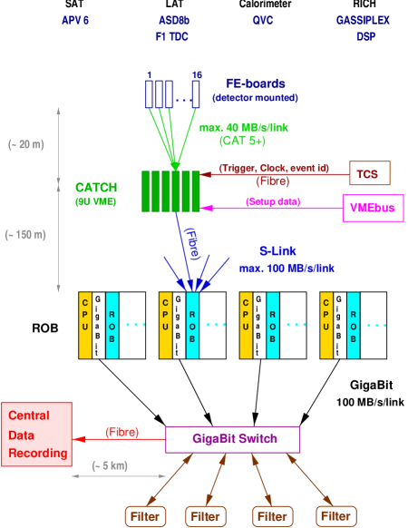
The digitized data are transmitted via CAT 5+ patch cables [2] at rates of up to from the front-end to FPGA based CATCH modules (CATCH = COMPASS Accumulate, Transfer and Control Hardware) which serve as readout drivers. The transmission between the front-end and CATCH modules is based on the serial protocol generated by the HOTLink chip [3]. The CATCH functions as a data concentrator and a pre-event builder as well as a control unit of data integrity of events sent from the front-end devices. Furthermore, the CATCH takes over automatic front-end initialisation and calibration tasks. The same module serves also as a remote fan-out for the COMPASS trigger distribution and time synchronisation system (TCS).
In the next hierarchical step of the data acquisition system the data are transmitted from the CATCH to large readout buffers (ROB) via S-link [4] connections. The ROBs are capable to store at least all data which have been collected during one spill. Again pre-event building and checks for data consistency are performed before the sub-events are transmitted via Gigabit Ethernet to filter computers. Here the final event-building is performed and complete events may be rejected based on physics constraints. Finally, the events will be transferred at a continuous rate of up to 35 MByte/s to the central data recording facilities at CERN where they are stored in object oriented federated databases for later off-line analysis.
The 1 Time Converter Core
Handling extremely high hit and data rates are the key feature of the COMPASS detector. Hitherto existing time converter chips were not designed to digitise six million or more hits per second with a precision of better then . In addition, this demanding task even has to be performed without any dead time during time conversion. Given the complexity of the task to design a new TDC chip which fulfils all COMPASS requirements the most evident approach was to develop the 1 chip as ASIC together with an industrial partner of outstanding experience and knowledge. The outcome of the fruitful collaboration with acam-messelectronic gmbh [5] is a state-of-the-art multi-purpose TDC chip with many different modes of operation in terms of functionality and resolution. To guide the reader through the technical description a schematic block diagram of the chip is given in Fig. 2. The technical specifications for the TDC are summarized in Table 1. The logic structure of the TDC architecture can be divided into the time measurement unit, the arithmetic logic executing the trigger correlated hit selection as well as the readout buffer and output interface.
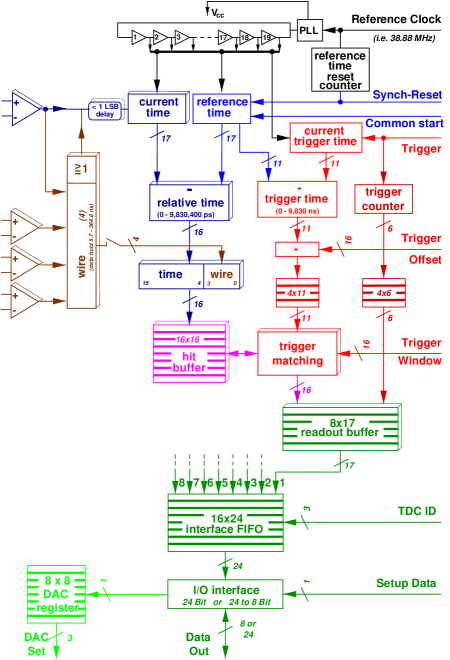
The clockwork of the 1 is an asynchronous ring oscillator consisting of 19 identical voltage controlled delay elements (see Fig. 3). The dynamic range of the delay chain is extended to 16 bits by a coarse counter. A time measurement with the 1 contains the combination of the status from the array of the delay chain and the coarse time counter. The leading and/or trailing edges of hits and the leading edges of trigger signals are sampled by this device without any dead time.
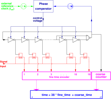
The process technology of 0.6 m sea-of-gates has a typical gate delay on the order of 100 to 150 ps depending on the batch of the production run, the ambient temperature and the supply voltage of the delay elements. To maintain stable gate propagation delays over extended periods a phase locked loop (PLL) is used to control the ring oscillator frequency. Thus the time measurement circuit maintains a constant time resolution and is tolerant to very large variations in temperature . The frequency of the ring oscillator and the time resolution of the 1, respectively, can be selected with two pre-scalers and (see Fig. 3). The ratio between the pre-scalers for the reference clock and the ring oscillator determines the cycle time of the asynchronous ring oscillator, which is 152 times the propagation time through a single delay element. Therefore, the user can chose the external reference clock freely between 500 kHz and 40 MHz.
Unlike a delay locked loop (DLL), a PLL filters any jitter of the reference clock signal. Therefore, no special precaution for the clock distribution system is necessary to provide the uncompromised high resolution of the TDC even in distributed applications. A carefully chosen floor plan together with the introduction of several separate power and ground supplies for the pad ring, high current output lines, and the time measurement unit are used to minimise the noise coupling.
The signal propagation of each input stage can be delayed by approximately 1 LSB divided in 64 individual steps. This feature can be used to improve the resolution of the TDC by a factor of two. In case the 1 is operated in the high resolution mode two neighboured input channels are connected internally and hence the original signal is split into two channels. The delay of one of the two signals is chosen such that it is half a LSB relative to its sister channel. This way additional phase information on the signal can be derived and be used to improve the time measurement to a resolution of . In this mode the dynamic range of the TDC is reduced by a factor of two.
The 1 as Latch Device
Another mode how to operate the 1-chip is the latch or hit mode. This mode is suitable for the readout of detectors which do not require precise time information for event pattern reconstruction but only time stamps for event building in a pipelined data acquisition system or for background suppression. Therefore it matches the requirements for MWPC readout or standard latch units and can be regarded as a cost efficient replacement of existing commercial products.
In the latch mode the number of input channels of the 1 is increased to 32. Each group of four of the 32 channels is connected to a fourfold input register and a logic OR which is linked to one of the eight time measurement channels of the 1 (see Fig. 2). When a hit arrives on one of four combined channels the next clock cycle of the asymmetric ring oscillator starts a counter. This counter, which defines the strobe length during which the registers accept input signals, is synchronous to the coarse counter, thus running with a period of , where refers to a typical digitisation bin size of the 1 in the standard resolution mode. After a pre-set time of the four inputs are switched to a second hit input register and a time stamp is taken with the full accuracy of the standard mode. The 12 most significant bits of the time stamp are placed in front of the four bits from the input register and transferred to the hit buffer. To ensure that no hits are lost while the input to the hit registers are switched both hit registers will accept signals during an overlap of about . Although it is desirable to have the overlap as short as possible small variations in production processes and the danger of efficiency gaps may require a longer overlap.
Data Sparsification
Digitized time stamps from hits are stored in dual port buffers. Each 1 channel has its individual buffer which can store up to 16 hits before it blocks further data input. The hit buffers are addressed in random access mode such that the trigger matching unit can search for data which belong to a coincident trigger. In the high resolution mode the hits are stored alternately in both hit buffers of the two channels. The procedure to store the data alternately permits higher data rates or longer trigger latencies because it is equivalent to double a single hit buffer to 32 words. A second advantage is the improved performance of the trigger matching unit since two units work in parallel on the data set in the hit buffers.
An arriving trigger signal is digitized by the same time measurement unit as the hit-signals. A programmable trigger latency time is subtracted from the measured trigger time to account for the time needed to form and to distribute the trigger to the distant front-ends. Trigger time-stamps are stored in a common four word deep FIFO until the arithmetic logic units are available to start with the trigger matching process. A programmable trigger window defined by the maximum time spread of a detector, e.g. drift time in wire chambers or time of flight, is loaded at the initialisation of the chip. A hit is considered to coincide with a trigger if its time stamp is within the latency corrected trigger time and the upper limit of the trigger window (see Fig. 4). Local bookkeeping of all triggers arriving at the 1 trigger input is handled by a six bit counter. In the case of a trigger buffer overflow the number of missed trigger signals can be reconstructed from a comparison of the trigger counter and from the trigger time stamps.
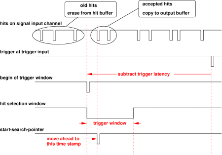
The search mechanism which is used in the trigger matching unit uses two independent pointers. The read pointer specifies the memory address currently being accessed to look for a hit which matches the trigger time. The start-search pointer marks the address where the search is supposed to start when the next trigger is loaded from the trigger FIFO. The start-search pointer is set to the read pointer position at the location of the first hit which matches the trigger time. All hits previous to this particular hit are deleted because they are outside of the future regions of interest. The selected hits are copied to the readout buffer. The search for further hits which belong to the same event is continued until either no more hits are stored or the next found time stamp in the hit buffer is younger than the region of the trigger window allows. Regions of interest for a sequence of triggers can overlap for those detectors which require long trigger windows. Therefore, selected hits are not deleted from the hit buffer when copied to the readout buffer.
When no triggers arrive for longer periods the write pointer may catch up with the start-search pointer. In this case new hits would not be accepted by the hit buffer anymore and the time stamps would be lost until the next trigger starts the clean-up process of the hit buffer. To avoid this, an artificial fake trigger is generated internally at regular intervals as soon as the trigger FIFO is empty. The fake trigger is handled like any real trigger except that no data are copied to the readout buffer. The generation of fake triggers helps to clean-up the hit buffer from old hits and guarantees unambiguous time measurements.
Readout
The introduction of dedicated readout buffers permits fast data readout while hits belonging to the next trigger are already selected in parallel by the trigger matching units. When the trigger matching process for a particular event is completed on all channels of a 1 the data ready signal is set and the output interface is prepared for readout. In case several chips are connected to a single front-end data bus the readout is controlled by a circulating token. The token control in the 1 has been optimised to avoid wait states when a token is handed over to the next chip.
The high speed readout interface of the 1 can be clocked with a frequency of up to . Two different modes for data readout are supported by the 1: 8 bit and 24 bit readout. The eight bit readout is used in the COMPASS experiment for applications where serial data interfaces and serial data links are used. The eight bit readout mode accords with the timing specifications of the HOTLink parallel to serial converter chip [3]. For a safe timing the 1 provides a bus-write-enable and a delayed bus clock with an adjustable skew for the HOTLink.
The 24 bit parallel readout can be used where highest data rates are anticipated and no data serializer is used. In this mode the user can exploit the full data throughput capabilities of the TDC chips.
TDC Initialisation
All data communications between the CATCH boards and the TDC front-end boards are exclusively serial. For the setup procedure, the TDC has a TTL serial data input which can be operated at a sustained rate of . The TDC serial interface is designed as a fourfold oversampling device. For different applications either the PLL reference clock or an optional dedicated setup clock can be used. The format for the setup data is characterised by two start and two stop bits, three bits for the chip address, a common address bit and four bits for register addresses followed by 16 bits for setup data. Since some data may be common for all chips on a board, these can be loaded in parallel by making use of the common address bit. In case of errors in the start or stop bits, the data reception is refused by the 1.
DAC Interface
In the COMPASS experiment the AD8842 octal 8-Bit digital-to-analog converter (DAC) [6] is used to control the thresholds of discriminators of some detectors. The AD8842 provides eight general purpose digitally controlled voltage converters with separate voltage inputs. Each AD8842 has its own register that holds the output state. The registers are updated from a 3-wire serial input digital interface.
The 1 is used to interface the serial setup lines from the CATCH to the DAC and to store the threshold values for multiple down-loads. The 1 contains eight registers of 1 Byte which may hold all register values for one AD8842. The data can be formatted and send via the 3-wire output interface to the AD8842. This operation does not interfere with normal TDC time conversion.
| Number of channels: |
| 4 for high resolution mode |
| 8 for standard resolution mode |
| 32 for latch mode |
| Digitisation bin size: |
| 75 ps for high resolution mode |
| 150 ps for standard operation mode |
| 5700 ps for latch mode |
| (typical values) |
| Reference-clock frequency: |
| Between 500 kHz and 40 MHz |
| (Clock is used for self calibration only) |
| Differential non-linearity: |
| Less than 0.3 LSB |
| Integral non-linearity: |
| Less than one time bin |
| Variation with temperature or supply voltage: |
| Less than one time bin |
| Dynamic range: |
| 16 bits |
| Double pulse resolution: |
| Typical 22 ns |
| Digitisation and readout dead time: |
| None |
| Hit buffer size: |
| 32 measurements for high resolution mode |
| 16 measurements for standard mode |
| 16 measurements for latch mode |
| Output buffer size: |
| 8 measurements |
| Common readout interface: |
| 16 measurements |
| Trigger buffer size: |
| 4 |
| Trigger latency: |
| up to full dynamic range of digitisation unit |
| (typical values: 9.8s, 4.9 s, standard, |
| high resolution mode, respectively) |
| Power supply: |
| 5.0 V |
| Power consumption: |
| 80 mA |
| Temperature range: |
| -40 to +85 degree centigrade |
| Hit input: |
| LVDS, LVPECL or TTL |
| Package: |
| 160 PQFP |
Acknowledgement
Our grateful appreciation goes to the local electronic workshop and engineer team, whose support during the development and production phase of the electronic components was essential. We also recognise the endeavours of our collaborators from the COMPASS collaboration and by the staffs of the collaborating institutions during several test periods at CERN. In particular we deeply appreciate the many stimulating discussions of our colleagues involved in front-end electronics development. The developments described in this report are supported by the German Bundesministerium für Bildung, Wissenschaft, Forschung und Technologie.
References
-
[1]
G. Braun et al., TDC Chip and Readout Driver
Developments for COMPASS and LHC-Experiments,
Fourth Workshop on Electronics for
LHC-Experiments, Rome, September 21-25 1998;
CERN/LHCC/98-36.
For further information see also:
http://hpfr02.physik.uni-freiburg.de - [2] ISO/IEC 11801:1995 Information technology – Generic Cabling for Customer Premises.
- [3] Cypress Semiconductor, CY7B923/CY7B933 HOTLink Transmitter/Receiver data sheet, Cypress Semiconductor High Performance Data Book, August 1, 1993.
- [4] E. van der Bij et al., S-LINK: A Prototype of the ATLAS Readout Link, Fourth Workshop on Electronics for LHC-Experiments, Rome, September 21-25 1998.
- [5] Address: acam-messelectronic gmbh, Haid-und-Neu Str. 7, D-76131 Karlsruhe; EMAIL: support@acam.de.
- [6] Analog Devices, Norwood, MA 02062-9106 Datasheet: AD8842, an 8-Bit Octal CMOS TrimDAC.
- [7] IEEE P1386, Standard for a Common Mezzanine Card Family: CMC.