HIGH RESOLUTION PIXEL DETECTORS FOR LINEAR COLLIDERS
Abstract
The physics goals at the future linear colliders require high performance vertexing and impact parameter resolution. Two possible technologies for the vertex detector of an experimental apparatus are outlined in the paper: an evolution of the Hybrid Pixel Sensors already used in high energy physics experiments and a new detector concept based on the monolithic CMOS Sensors.
1 Introduction
Precision measurements of Top quark and Higgs boson physics are in the reach of the
next generation of linear colliders, operating at a centre of mass energy
ranging from the pole to .
High granularity, impact parameter resolution, secondary vertex
reconstruction and jet flavour tagging are the
essential tools for these measurements and define the figures of merit for a Vertex Detector.
In the 1996 Joint DESY/ECFA study, the minimal requests on the impact parameter resolutions in the plane and along the beam direction were defined to be [1] and with a total material budget below for the complete Vertex Detector, fitting between the beam pipe originally at a radius and the intermediate tracker starting at . Conceptual design of vertex trackers based on hybrid pixel sensors [2] and CCD’s [3] were proposed and Research & Development plans defined.
Since then, several analysis remarked the advantages of possibly improved performances, both in terms of asymptotic resolution and multiple scattering. This triggered the quest for lightweight technologies that could provide space point informations along the particle track with at least resolution. At the same time, an improved final focusing scheme allowed to shrink the beam pipe to radius, with the inner sensitive layer at .
In the following, two possible detector technologies are presented: the former is based on the development of the Hybrid Pixel Detectors used in DELPHI [4] and WA-97 [5] and being finalized for the LHC experiments [6, 7, 8]; the latter is based on the evolution of monolithic CMOS imagers [9] to achieve the sensitivity to minimum ionizing particles.
2 Hybrid Pixel Detectors
2.1 General concepts
The achievement of a resolution in a Silicon detector can be accomplished probing the diffusion of the charge carriers locally generated around the impinging particle trail. Given the diffusion characteristics, this require a microstrip or pixel pitch well below and an analog output to interpolate the signals on neighbouring cells.
While this is feasible with the 1d microstrip detectors [10], the need to integrate the front-end electronics in a cell matching the detector pattern defines the ultimate pitch in 2d pixel detectors. At the moment, the most advanced read-out chips have a minimum cell dimension of , produced in 0.8 CMOS technology, implemented in a rad-hard process. On one hand, the trend of the VLSI development and the recent studies [11] on intrinsic radiation hardness of deep submicron CMOS technology certainly allow to assume a relevant reduction in the cell dimensions on a mid-term. On the other hand, a detector design overcoming this basic limitation is worth being considered.
What is being proposed is a layout inherited from the microstrip detectors [12] where it is assumed to have a readout pitch n times larger than the pixel pitch (see for instance fig. 1 for ). In such a configuration, the charge carriers created underneath an interleaved pixel will induce a signal on the output nodes, capacitively coupled to the interleaved pixel. In a simplified model where the detector is reduced to a capacitive network, the ratio of the signal amplitudes on the output nodes at the left hand side and right hand side of the interleaved pixel (in both dimensions) should have a linear dependence on the particle position. The ratio between the inter-pixel capacitance and the pixel capacitance to backplane plays a crucial rule in the detector design, as it defines the signal amplitude reduction (an effective charge loss) at the output nodes and at last the sustainable number of interleaved pixels. Recent results [13] on readout pitch microstrip detectors have been published, and a resolution has been achieved in a layout with 3 interleaved strips ( strip pitch) and for a . Similar results may be expected in a pixel detector, taking into account a lower noise is achievable because of the intrisically smaller load capacitance and the charge is possibly shared on four output nodes reconstructing the particle position in two dimensions. Improvements are certainly possible sampling the diffusion with a smaller pitch.
2.2 Detector prototypes and electrostatics characterization
Prototypes of detectors with interleaved pixels have been designed in 1998 and delivered in january 1999.
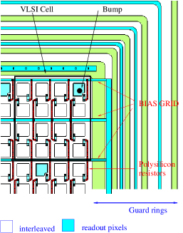
The layout of one of the structures is shown in fig. 1. A series of guard rings defines the detector sensitive area. A bias grid allows the polarization of the interleaved pixels too; each implant is connected to the metal bias line by polysilicon resistors in the range. A metal layer is deposited on top of the pixels to be connected to the VLSI cell. The backplane has a meshed metal layer to allow the use of an IR diode for charge collection studies. In a 4” wafer 36 structures were fit, for 17 different layouts; a VLSI cell of or was assumed and detectors with a number of interleaved pixels ranging between 0 and 3 and different areas were designed.
Ten high resistivity wafers were processed 222at the Institute of Electron Technology, Warszawa, Poland together with an equal number of low resistivity wafers for process control, the details of which have been outlined in [14]. Two wafers were retained by the factory for a destructive analysis and two others were stored for later use. All of the structures on five undiced wafers were visually inspected, tested up to and characteristics I-V and C-V curves produced; the results may be summarized as follows:
two wafers suffered from processing problems. As a consequence of it, one wafer had a high leakage current () even at very low voltages on most of the structures; the second wafer had interrupted metal lines, making the bias grid inefficient. The former problem is possibly connected to the Al pattern plasma etching; the latter to a not optimal planarization of the device.
three wafers had extremely good characteristics, with a mean current at full depletion. Structures were classified as good detectors if no breakdown was observed below , the leakage current at depletion voltage was below with a smooth trend vs. the applied voltage and no faults in the line pattern were detected by visual inspection. According to these criteria, 55/89 structures were accepted. In fig. 2 the value of the currents and detector capacitances at depletion voltage are shown for all of structures in one of the three wafers. In fig. 3 the typical and curves are shown.
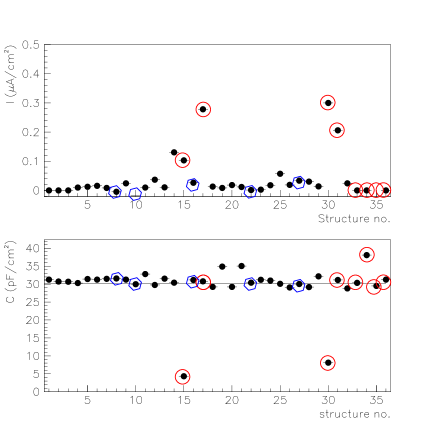

While the curves behave as expected, the current has a peculiar trend. After a plateau is reached at full depletion, the current takes off at values in the range. For most of the structures it is a mild increase, but most of the rejected detectors are characterized by a steep slope, eventually ending with a breakdown below . Independent measurements of the guard ring and bias grid current has shown the latter is responsible for the increase, that might be connected to sharp edges where the electric field achieves high values. A full device simulation is planned to help understanding this feature.
2.3 Outlook
The prototypes have not shown any design fault even if processing and layout optimization has to be considered. On a short term, measurements of the inter-pixel and backplane capacitances are planned, completing the electrostatics device characterization. A charge collection study will follow, relying on a low noise strip detector analog chip and an IR light spot shone on the meshed backplane. These measurements will be a proof of principle of the proposed device and define the fundamentals for a further iteration, aiming at a pitch.
The device thickness is a particularly relevant issue for the application of Hybrid Pixel Sensors in a linear collider experiment. The minimal thickness is defined by both the detector performances and the backthinning technology for bump bonded assembly. Industrial standards guarantee backthinning down to and a procedure to obtain thin Hybrid Pixel detectors is being tested [15]. The small load capacitance of the pixel cells shall guarantee an extremely high . Scaling what was obtained for microstrip detectors, the desired resolutions might be obtained with a thick detector (a () thick assembled device). Moreover, the mechanical structure of a three layer vertex detector based on Hybrid Pixel Sensors is being designed and a realistic material budget evaluated.
3 Monolithic Pixel Sensors
3.1 General concepts
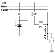
In the early 90’s monolithic pixel sensors have been proposed as a viable alternative to CCD’s in visible imaging [9]. These sensors are made in a standard VLSI technology, often CMOS, so they are usually called CMOS imagers. Three main architectures have been proposed, namely: Passive Pixel Sensors (PPS) and Active Pixel Sensors (APS) with photodiode or photogate. In the former, a photodiode is integrated in each pixel together with a selection switch, while in the latter (fig. 4), three transistors are usually integrated together with a photosite.
Today, most of the sensors are based on APS because of their superior noise performances: electron noise can be as low as r.m.s. at room temperature.
The use of standard CMOS technology gives APS several advantages with respect to the more generally used CCD’s: they are low cost; inherently radiation hard; several functionalities can be integrated on the sensor substrate, including random access; they consume very little power as the circuitry in each pixel is active only during the readout and there is no clock signal driving large capacitances.
Because of these characteristics, CMOS sensors are the favoured technology for demanding applications which are typically found in space science.
3.2 CMOS sensors for charged particle detection
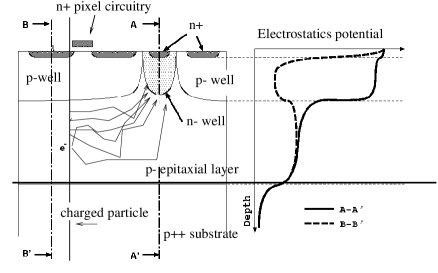
In visible light applications, special care is taken to maximise the fill factor, i.e. the fraction of the pixel area that is sensitive to the light. Because of the transistors, fill factors in CMOS sensors are relatively low (in the order of 30%). This can be a severe limitation in high-energy physics application, if no special care is taken. One of us [16] proposed to integrate a sensor in a twin-well technology with an n-well/p-substrate diode in order to achieve 100% fill factor for ionizing particle detection (fig. 5). This technique has already proven its effectiveness in visible light applications [17] reducing the blind area to the metal lines, opaque for visible light but not for charged particles.
CMOS sensors could achieve high spatial resolution: the pixel size is usually between 10 and 20 times the Minimal Size Feature of the used technology, which means that pitch is possible, and hence spatial resolution better than even with a binary readout. At the same time, very low multiple scattering is introduced as the substrate can in principle be thinned down to a few microns. A charge particle CMOS detector would also benefit from the generic characteristics of these devices, including low power dissipation, radiation resistance of deep submicron CMOS technologies and low cost.
3.3 CMOS sensors for a Linear Collider
In order to prove the effectiveness of CMOS sensors for the Next Linear Collider, an R&D program has been initiated by the Strasbourg group. Some existing commercial devices are currently under test. Since the performances of the sensors depend on details of the fabrication process, a full-custom design of a first prototype sensor (MIMOSA = MIP MOS APS) has been done in a CMOS technology. The circuit will be back from the foundry in autumn 1999.
A preliminary detector design of a Microvertex Detector based on CMOS sensors was also completed. The detector is supposed to be made of 5 layers, the inner most having a radius of 1.2 cm. It is made of a cylindrical barrel part associated to forward and backward conical and disk-like extensions , intercepting with at least 4 layers charged particles produced at polar angles ranging from 6 to 174 degrees. The sensors are assumed to be thick squares of area, with an active surface close to 80%. Assuming a few per-cent overlap between the active surfaces of neighbour sensors, about 5500 units are needed to cover the area of the detector. Since the sensors have low power dissipation, a mechanical support made of thick, large, thermal diamond rods was considered. A detailed simulation showed that such a device, connected to a light system of thin cooling pipes, would provide enough thermal conduction by itself to evacuate the heat from the sensors, thus substantially reducing the material seen by the particles. The simulation of the mechanical constraints showed that the bending of the rods should nowhere exceed a sagitta. As a further advantage, diamond aluminised with a few micron thick layer could fan in/out all the electrical signals. Globally, the material budget is such that particles crossing the 5 detector planes would in average see a total amount of 0.8% radiation length in the barrel and 2.9% in the forward-backward parts, values making the CMOS sensor based vertex detector very competitive.
4 Conclusions
Two detector technologies suitable for a Vertex Detector at the next generation of colliders have been presented in the paper. Hybrid Pixel Sensors could achieve the desired performances overcoming the limitations defined by the electronics cell dimension, mating the pixel, and developing a dedicated analog readout chip. Charge sharing and S/N ratio are the critical issues for these detectors as they determine both the resolution and the minimal detector thickness. Detector prototypes have been produced; the electrostatics characterization is ongoing and the first results are positive. Monolithic CMOS sensors could achieve an excellent resolution introducing a very low multiple scattering. Impressive results as visible light detectors have been recently obtained and a custom designed device optimized for ionizing particles have been submitted.
References
References
- [1] R. Settles ed., DESY 97-123E, (1997).
- [2] M. Battaglia et al., DESY 97-123E, 641-658 (1997).
- [3] C.J.S. Damerell et al., DESY 97-123E, 659-666 (1997).
- [4] P. Chochula et al., NIMA 412, 304 (1998).
- [5] Di Bari et al., NIMA 395, 391 (1997).
- [6] ATLAS collaboration, The Pixel Detector Technical Design Report, CERN-LHCC 98-13, (1998),
- [7] D. Bortoletto, FERMILAB-CONF 98-196, 22 (1998).
- [8] F. Antinori, FERMILAB-CONF 98-196, 41 (1998).
- [9] E.R. Fossum, IEEE Trans. Electron Devices 41, 452 (1994).
- [10] A. Peisert, in Instrumentation in high energy physics, World Scientific, 1 (1992).
- [11] W. Snoeys, CERN-LHCC 97-60, 139 (1997).
- [12] J.B.A England et al, NIM 185, 43 (1981).
- [13] M. Krammer and H. Pernegger, NIMA 397, 232 (1997).
- [14] W. Kucewicz et al, in the proceedings of the Krakow Epiphany Conference on Electron-Positron colliders, january 6-9, 1999; to be published on Acta Physica Polonica.
- [15] T.E. Browder et al., FERMILAB-CONF 98-196, F (1998).
- [16] R. Turchetta, presentation at the 2nd SOCLE Meeting, Paris (France), January 28, 1999
- [17] B. Dierickx, G. Meynants, D. Scheffer, in the proceedings of the IEEE CCD & AIS workshop, Brugge, Belgium, 5-7 june 5-7 (1997)