GLAS–PPE/95–04
R.L. Bates??) C. Buttar??) S. D’Auria??) C. del Papa??) W. Dulinski??) S.J. Gowdy??) S. Manolopoulos??) V. O’Shea??) T. Sloan??) C. Raine??) K.M. Smith??) F.K. Thomson??)
On Behalf of the RD8 Collaboration
A gallium arsenide detector was tested with a beam of 70GeV pions at the SPS at CERN. The detector utilises a novel biasing scheme which has been shown to behave as expected. The detector has a pitch of 50m and therefore an expected resolution of 14.5m. The measured resolution was approximately 14m. By using a non-linear charge division algorithm this can be increased to 12m. Noise was the limiting factor to the resolution. This was 2000e- as opposed to the expected 360e-. This noise is also thought to have reduced the detection efficiency of the detector. The source of the excess noise is currently being investigated.
Presented by S.J. Gowdy at the
workshop on GaAs detectors and
related compounds
San Miniato (Italy) 19-21 March 1995
1 Introduction
As part of the ongoing programme developing radiation hard detectors for the LHC a test beam run was carried out in September 1994.
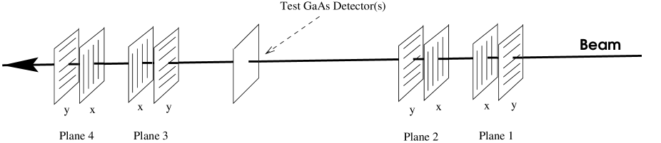
2 Testbeam Setup
The X1 beam from the SPS at CERN was incident on a telescope provided by L.E.P.S.I., Strasbourg. This beam was a tertiary beam: pions with an energy of 70GeV were used for the test. This telescope employs eight silicon microstrip detectors and five trigger scintillators. The silicon detectors had a 25m implant pitch, but strips were only read-out every 50m. The intermediate implant strip produces enhanced resolution between the strips. Each of these detectors was 300m thick. A schematic representation of the telescope can be seen in figure 1.
The silicon detectors and the test detector were read out with a Viking pre-amplifier chip[1]. This produces a multiplexed signal which is sampled with a Sirocco ADC and then written to an EXABYTE tape. The Siroccos and the tape drive are housed in a VME Data Acquisition (DAQ) system. This allowed limited on-line analysis.
For an event to be written to tape it had to satisfy the trigger conditions, namely that the event occurred during the beam extraction phase of the SPS, the DAQ was not BUSY and finally, and most importantly, there were coincident hits in a number of the scintillators.
3 Detector Structure
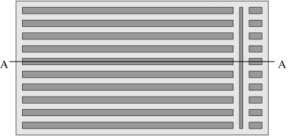
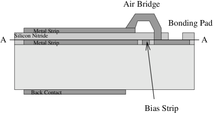
The gallium arsenide detector tested was fabricated by Alenia SpA, Rome. It had both 50m pitch and readout. The detector had an integrated Si3N4 capacitor and novel biasing scheme to keep the detector strips close to zero volts. The capacitor was between two layers of metal, the lower was in contact with the substrate and was 30m wide and the upper was 20m wide. The cross-section of a detector and an illustration of the top of the detector are shown in figure 2.
The gap between the biasing strip and the detector strip was 5m long and 6m wide. The thickness of the detector was 200m.
4 Detector Characteristics
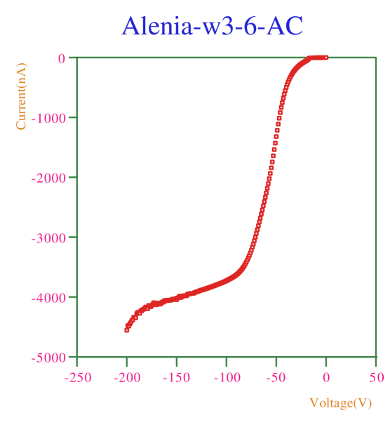
Before the detectors are tested in a beam they are characterised electrically. The basic test for a detector is to verify that it operates as a reverse-biased diode with acceptable current. The I-V characteristic is shown for the detector in figure 3.
To test the novel biasing structure the voltage on the detector strip was plotted against the voltage applied to the rear contact, using the circuit shown in figure 4(a).
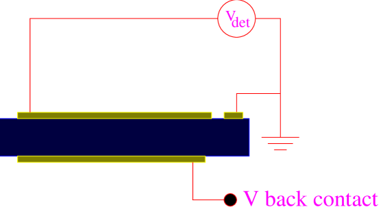
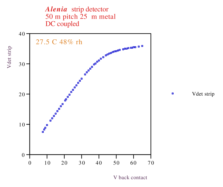
The results of the test show that with the biasing strip held at zero volts the detector strip will float up to about 35 volts. Therefore, during the testbeam this strip was held at -30V. The results are shown in figure 4(b).
5 Off-line Analysis
The off-line analysis consisted of two separate stages. The first of these read in the RAW data. The first 100 events are used to determine the pedestal levels of the data and the next 100 to determine the noise. This program also allows for a group of pedestals shifting coherently, in what is known as Common Mode Shift(CMS).
After the initialisation phase the noise is continuously updated, with a weight of 50 on the old value to reduce the effect of actual hits which fall below the cut on the noise. It then looks through the remaining data for clusters.
A cluster is found if the value for any strip is above 3(4). A search is then made for any adjacent strips with above 1.5(2). If found, these determine the width of the cluster for GaAs(Si); the cluster total signal and noise are then calculated using equations 1 and 2.
| (1) |
| (2) |
If the cluster is wider than a single strip, its value is evaluated using equation 3. This is used to enhance the resolution using a non-linear charge sharing algorithm.
| (3) |
In this equation () is the signal on the left(right) of the the two maximum pulse height strips of a cluster. A typical distribution from a silicon detector is shown in figure 5(a).
By integrating the distribution we define a look-up table for the position of a hit between the two strips. The integrated distribution is shown in figure 5(b).


The cluster information is then written to a DST file together with the pulse height and noise values for the five strips on either side of the cluster centre.
This file is then read in by the track fitting program. It uses the hits in the DST file to determine the relative alignment of the detectors. First, the telescope is self-aligned with its origin at the centre of the first two detectors.
Next the test detectors are aligned in this reference frame. The first stage is carried out by centering the residual plot for the detector around zero. Then, to allow for the strips not being orthogonal to the reference frame, the residual in the detector is plotted against the position along the strip. This plot is shown in figure 6(a). A linear fit is made to the data and the hits rotated to align the strips with the reference frame.


After this is complete the detector position along the beam line is adjusted so that the fit residuals are minimised. The detector is then rotated by a small angle about the centre strip axis and the residuals are minimised again.
6 Results
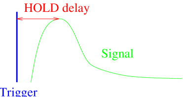
The shaping time for the gallium arsenide was reduced from the standard silicon time of 2100ns to 680ns to reduce the noise as the parallel noise term is expected to dominate with gallium arsenide. This is implemented by a potentiometer on the repeater card. On the DAQ this shaping time is stored as the HOLD delay and is the time from receiving a trigger to the expected peak in the signal, as illustrated in figure 7. During the test beam run there can be only one value for all detectors: this number was varied between 1000ns and 680ns to optimise the readout for the gallium arsenide detector under test. Some degradation of the silicon performance was accepted due to the reduced shaping time.
The equivalent noise charge(ENC) was measured to be 2000e-. The signal-to-noise from the data in all cases was very close to 6 (Figure 8(b)). The signal was therefore 12000e-, which implies a charge collection efficiency(CCE) of 46%. This is in good agreement with tests made on pad diodes which have 60% CCE but were operating at 200V as opposed to 180V as used in the test beam.


The rms of the residual distribution shown in figure 8(c) corresponds to a detector resolution of m. Figure 6(b) shows that this is constant along the length of the strips. This compares well with the expected resolution from binary read out, that is without charge-sharing information, as given by .
Using only clusters with a width of two or more strips, the resolution improves to approximately 12m. It is observed that 50% of events have clusters of more than one strip, which is slightly more than expected from the gap to metal width ratio, indicating a proportion are due to noise.
The detection efficiency at the shortest HOLD delay time was 47%. This was the highest value obtained. Various investigations were carried out on the data in an attempt to determine the source of this poor performance. A search was made for inefficient regions in both time and space. However, none were found.
The low detection efficiency may be attributable to a problem with the DAQ which produced an asymmetric distribution for the silicon detectors which had been normal before this test beam run. At present, however, it is not possible to prove that this is the sole cause of the inefficiency.
7 Simulation
To investigate other possible reasons for the poor detection efficiency, a computer simulation was done. The simulation program produced data in the RAW format produced by the DAQ system, thus serving also as a test to validate our use of the software.
In this simulation charge sharing is assumed to be linear in all detectors. The charge deposited by a particle is then shared between two strips. This charge is determined from a function which produces a Landau distribution of signals. Once this has been shared between the two strips Gaussian noise is added to all strips.
The resulting is shown in figure 9(a). It appears that, for a value below approximately ten, the detection efficiency drops dramatically.
This is due to the charge sharing dividing the signal and a conspiracy of noise and Landau fluctuations pushing the signal below the threshold of 3.
This would occur more readily toward the centre of the gap between the strips, as observed in the simulation (shown in figure 9(b)), however this was not seen in the actual data.


8 Conclusion and Further Work
The noise observed in the test beam data and with the detector in the laboratory is over five times greater than expected (360e- ENC[1]). The source of this excess noise will be investigated further.
By reducing the noise both resolution and detection efficiency will improve. The lack of resolution attainable with a given algorithm is proportional to [2]. As seen in figure 9(a), once the is above ten detection efficiency should not be a problem.
At the LHC gallium arsenide detectors will be aided by the faster shaping times of the pre-amplifiers, as 80% of the signal will be delivered within 20ns.
Currently under investigation are non-minority carrier injecting ohmic contacts which will enable detectors to be more easily “over-depleted”. This will increase the charge collection efficiency of the detectors and hence the signal produced.
Studies to be made in 1995 include varying the gap/metal width ratio, response at lower temperatures and keystone detector geometry. In varying the gap/metal width the signal will decrease (due to poorer field) but the resolution will increase. Since silicon detectors may require an operating temperature of -10∘C to prevent reverse annealing the gallium arsenide response at lower temperatures needs to be checked. It is planned to use detectors with keystone geometry in the ATLAS forward region so detectors must be fabricated in this design to prove their viability.
9 Acknowledgements
Off-line software was originally written by R. Turchetta, J.A. Hernando and J.A. Straver, to all of whom the authors are greatly indebted. A. Rudge and R. Boulter also provided exceptional technical support.
References
- [1] O. Toker et al. Viking, A CMOS Low Noise Monolithic 128 Channel Frontend For Si-strip Detector Readout. CERN, PPE 93–141, July 1993.
- [2] R. Turchetta. Spatial resolution of silicon microstrip detectors. Nuclear Instruments and Methods in Physics Research, A335(1993):44–58.