HEP-EX/9507013
An Investigation into the Radiation Damage
of the Silicon Detectors of the H1-PLUG Calorimeter
within the HERA environment
W. Hildesheim111Deutsches Elektronen Synchrotron, Hamburg, M. Seidel222I. Institut für Experimentalphysik, Universität Hamburg
Abstract
The silicon detectors used in the H1-PLUG calorimeter have shown increasing aging effects during the ’94 run period of the electron proton storage ring HERA. These effects were particularly manifest as degradation of the signal to noise level and the calibration stability. The reasons for this behaviour have been found to be correlated with radiation damage to the silicon oxide passivation edges of the detectors in strong and fluctuating increases of the leakage currents and in severe changes of the flat band voltages. Depletion voltages however are found to be stable and therefore bulk damage of the silicon can be excluded. A comparison with measurements made by thermoluminescence dosimeters as well as related laboratory experiments suggest that the aging is due to very low energetic electrons and photons.
1 Introduction
Silicon detectors are being increasingly applied to high energy physics experiments. Silicon technology has been choosen by experiments for purposes as different as the construction of vertex detectors, trackers and calorimeters. As an example the ATLAS collaboration [1] at the future LHC will instrument the complete inner part of their detector with silicon. One reason for this is the high radiation hardness of silicon which is a requirement for all present and future accelerators. Two special collaborations at CERN, RD2 and RD20 currently investigating all problems related to radiation hardness [2], [3], are focussing on hadronic radiation damage.
The H1-PLUG-calorimeter is the first hadronic silicon instrumented sampling calorimeter and has been operational since ’92 within the environment of the HERA electron proton collider. Severe radiation damage of the silicon detectors used has been observed in particular during the ’94 run period after a strong increase of the delivered luminosity. The observed radiation damages will be presented and discussed in this paper.
Following the description of the PLUG calorimeter (sect. 2), the basic characteristics of the silicon detectors used are presented (sect. 3). The PLUG readout circuit is explained (sect. 4) as an introduction into the experimental difficulties of the monitoring of the diode characteristics during normal PLUG operation (sect. 5). The results of the monitoring during the ’94 run period of HERA are given (sect. 6), and are compared with the final analysis of related measurements as performed in the laboratory (sect. 7). The results are finally discussed in section 8.
2 PLUG Calorimeter Description
The PLUG subdetector of H1 is a silicon instrumented sampling calorimeter, designed to fill the gap between the forward part of the LAr calorimeter and the beam pipe and thus to ensure the hermeticity of the energy measurement [4]. In recent applications the PLUG has proved to play an important role for the tagging of rapidity gap events [5].
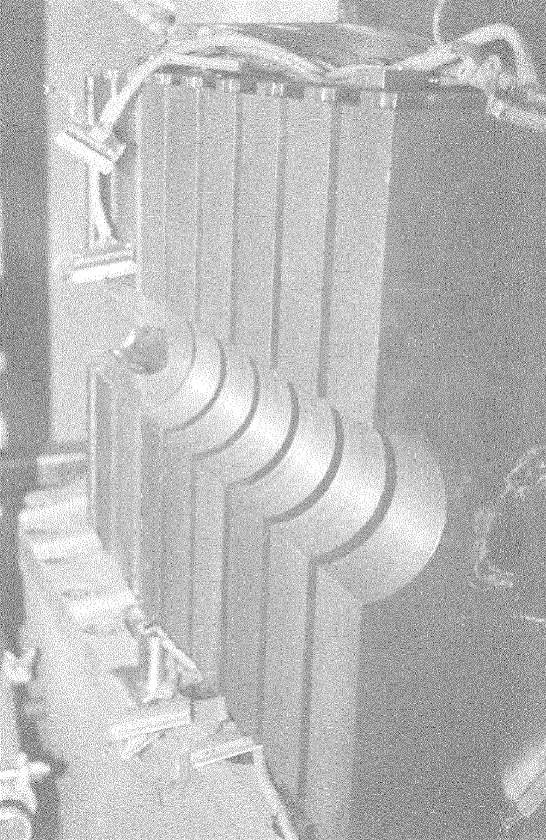
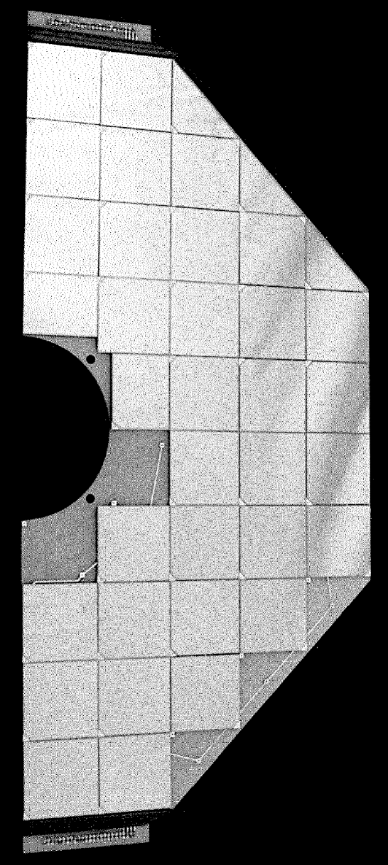
The PLUG is mounted in the return yoke of the magnet, one half is shown in the left part of figure 1 with the slots in between the copper absorbers visible for the 8 detector modules. The inner part of such a module is displayed in the right part of figure 1. It is instrumented with a total number of 42 detectors most of which are square shaped (5 x 5 ) complemented by rectangular wafers close to the beam pipe and triangular ones at the outer rim. All detectors have a total thickness of arround 400 [6]. The silicon detectors are fabricated in our own laboratory using a unique combination of a Schottky barrier process and planar technology [7].
The PLUG calorimeter is instrumented with a total number of 8 planes (16 modules), each containing 84 detectors and thus consists of ideally 672 detectors (see table 1). For maintaining simplicity and cost effectiveness it was not feasible to use a read out system with this large number of individual electronic channels. Instead two detectors situated in neighbouring planes along the beam axis, but at the same radial position, are ganged together, thereby reducing the number of electronic channels to 336. For similar reasons, several detectors in one module (i.e. on the same read out board) are connected to a single voltage supply channel. In total 80 such channels are used 333CAEN modules (A336P, A436A) are used.
| S | T | R | total | |
|---|---|---|---|---|
| 90 | 55 | - | - | 55 |
| 91 | 167 | 21 | 9 | 197 |
| 92 | 182 | 51 | 19 | 252 |
| 93 | 108 | - | 36 | 144 |
| sum | 512 | 72 | 64 | 648 |
3 Basic Characteristics of the Used Silicon Detectors
The capacitance of a silicon detector with area A and a depleted thickness X (depth of the electric field) is simply given by eq. (1), where and .
| (1) |
X is a function of the applied reverse bias voltage V according to eq. (2)
| (2) |
where e is the elementary charge and the effective impurity concentration of the base silicon material. For the depletion of the total detector thickness d we get from eq. (2) the necessary bias voltage.
| (3) |
The voltage dependance of the detector capacitance is hence given by
| (4) |
In this simple description for a Schottky barrier diode we have neglected the ”built in” voltage which should have to be added to the external bias voltage V but is usually quite small (appr. 0.5 V) compared to the depletion voltage (around 50 V for our detectors).
Due to the fact that the front electrode partially overlaps the oxide passivated edge of the silicon detector, the C-V (capacitance/voltage) characteristic given by eq. (4), has to be modified for low voltages. This overlapping ”field plate” region forms a MOS (Metal-Oxide-Silicon) capacitance in parallel to the diode itself.
For voltages smaller than the ”flat band voltage” we still have an accumulation layer underneath the interface and due to the extremely small thickness of the silicon oxide passivation layer (appr. 2000 Å) the MOS-capacitance (to be added to the diode capacitance of eq. (4)) is very high. The silicon bulk below the field plate only becomes depleted once the external bias voltage exceeds the flat band voltage : the C-V characteristic is then dominated by eq. (4). Depending on the thickness and quality of the oxide passivation typical flat band voltages range betweeen 1 and 5 V and are hence not problematic with respect to the much higher operation voltages.
The other important performance parameter of the silicon detectors is the reverse current , which is in our case composed of three main contributions. Normally dominant is the bulk part, which is caused by thermal electron–hole–pair generation throughout the depleted volume of the detector. According to its thickness (eq. (2)) we get
| (5) |
and for a constant value of . is the temperature dependant generation current density. In addition to the simple behaviour of eq. (5) we have two surface contributions. One is related to the –Si interface of the field plate region of the detector rim. Above the flat band voltage the interface states located there, which also act as generation centres for electron–hole–pairs, become accessible to the electric field and hence contribute to the overall reverse current. Normally this is seen as a certain jump in the I-V (current/voltage) characteristic at the flat band voltage. The size of this effect is proportional to the overlapping field plate region and depends also on the quality of the oxide (concentration of interface states). The second contribution to the reverse current is due to the Schottky barrier itself. In contrast to the interface generation, this part exhibits also a certain voltage dependence and the size of its contribution is governed by the ”barrier height” which is a measure of the Schottky barrier quality. For more details on both C-V and I-V characteristics see [7].
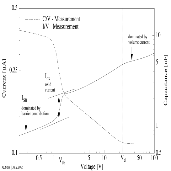
In the figures 3 and 3 the features discussed above are shown for a typical PLUG detector after all technological process steps have been completed but prior to being used during actual beam runs. Figure 3 visualizes the principal electric field extension at the detector edge below and above flat band voltage, the C-V and I-V characteristics are shown in fig. 3. In the given example the flat band voltage turns out to be 1.5 V. This is both seen in the dramatic decrease of the detector capacitance and the jump of the reverse current at that point. For larger voltages the capacitance turns out to be inversely proportional to as to be expected by eq. (4) and reaches its geometrical limit of 630 pF at the depletion voltage (), while the current saturates at the same point.
4 PLUG Readout Circuit
The readout circuit of the PLUG calorimeter was designed in such a way that a maximum of vital information about the individual silicon detectors could be obtained during the beam period. Specifically the voltage needed to extend the electric field throughout the detector thickness and hence to ensure the total collection of charge generated by a penetrating particle, should be checkable at any time. This depletion voltage can however not be measured as in the laboratory by using e.g. a capacitance bridge. Instead the response of the readout circuit to a given charge injected by a testpulser is used. Details are given below.
Another similarly important parameter is the reverse current of each silicon detector. Only if this value is known one can calculate the voltage drop across the bias resistor and hence ensure that the net detector bias voltage stays sufficiently above the depletion voltage. As two detectors situated in successive planes (modules), but at the same position are ganged together for readout and up to 14 detectors in one single plane are connected to one bias channel (see section 1), the monitoring of both the C-V and I-V characteristics for individual detectors imposes a significant difficulty, which finally led to the following compromise solution.

In fig. 4 a simplified circuit diagram of one read out channel is shown. The signal output of two detectors located in adjacent planes, for instance in the first and second, but at the same r, position of the calorimeter, are connected to one preamplifier. An appreciable ganging had also to be used for the bias supply of all 672 detectors from only 80 available bias channels. Unfortunately a bias distribution box, as used for the LAr calorimeter had to be ruled out because of unacceptable limitations for the detector current. Due to the exposed position of the PLUG calorimeter in the very forward angular range, some radiation damage had to be expected with resulting larger increase of the reverse current for the innermost detectors closest to the beam pipe. In order to achieve a similar accuracy in current monitoring throughout the calorimeter, a bias ganging of only 3 detectors was foreseen for the innermost detectors, extending to a connection of up to 14 detectors to one bias supply at the outer rim. At a given operational voltage each detector may be symbolized by its capacitance and the reverse current by a parallel resistor . A common filter network for the detectors, belonging to one bias module, is used for the reduction of low frequency noise picked up via the long bias transfer line between the unit located in the electronic trailer of the H1 experiment and the PLUG. The individual bias resstors on the other side of the detectors enable the signal readout via the likewise individual coupling capacitors . For calibration purposes a charge is induced via the charge terminator capacitance . It has to be noticed, that the actual realisation of the block diagram is contained in 5 different electronic units (indicated by dotted lines in fig. 4) connected by cables of varying length. The bias unit and the pulser crate are located in the electronic trailer, the adapter box ADBX (bias distribution and readout ganging) and the analog box ANBX sit behind the return yoke of the magnet and the PLUG calorimeter itself.
Especially the cables between the detectors and the coupling capacitors together with any inherent stray capacitance add a constant value of to the voltage dependent detector capacitance . Thus in fig. 4 is the sum of both these values.
| (6) |
5 Monitoring of Diode Characteristics
In this section we will descibe the possibilities for monitoring the current, capacitance and noise characteristics of the installed detectors even during luminosity periods. The principal difficulty here is that due to the necessary ganging described above, the individual detector performance cannot be measured. The following discussion is given for one bias channel i only; its index is omitted.
5.1 Reverse current
As detectors (n=3-14, see section 4) are connected to one bias supply unit, we cannot measure the individual detector currents but have instead to assume that the measured current is equally distributed, resulting in :
| (7) |
Hence the net bias voltage for one detector is estimated to be
| (8) |
Equations (7) and (8) enable us to measure the I-V characteristics for each detector. We add here that the correction due to the voltage drop across the common resistor is exact. However the term due to the individual preamplifier bias resistor is sensitive to the assumption of eq.(7) and may be particularly important if the measured current is very large.
5.2 Detector capacitance
The C-V characteristic for each individual detector can be investigated by measuring the signal height for a given input charge as function of the detector voltage. A charge is induced by the test pulser via the charge terminator . Taking the values of the different capacitances into account (fig. 4), the response of the preamplifier can be calculated according to the equivalent circuit diagram of fig. 5. This results in the following relation
| (9) |
where is the input charge for the preamplifier. Thus the output signal is given by eq.(10), where is replaced by the expression of eq.(6).
| (10) |
Using eq.(4) and the discussion in section 2 the voltage dependence of the signal can be finally represented by :
| (11) |
It should be mentioned that the same uncertainties for the voltage corrections as discussed for the I-V characteristic according to eq.(8) are relevant here too.
5.3 Signal noise
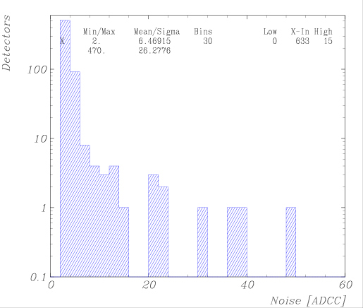
The signal noise can only be measured for each electronic channel, connected to two detectors ganged together as seen in fig. 4. Capacitance and noise characteristics are measured simultaneously. For the capacitance we use the mean value of the signal distribution and the noise is extracted from its standard deviation. The noise performance contains two contributions, one of which is due to the input capacitance of the preamplifier and the second corresponds to the detector noise. For newly commissioned detectors the second contribution is negligible. Hence the combination of I-V (ganging in one plane) and noise-characteristics (ganging of two detectors in two consecutive planes) provides a tool to identify single bad detectors.
6 Measurements during HERA operation
The measurements taken during the 1994 HERA operation period are presented. The section is subdivided into the results concerning the reverse current, the detector capacitance, the signal noise and the absorbed radiation dose. These parameters have been monitored for each of the 648 detectors during the whole ’94 run-period.
6.1 Reverse Current
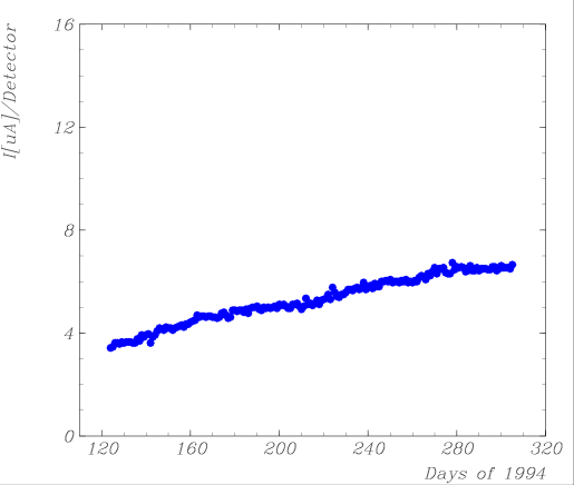
In figure 8 the reverse current as a function of time given in days is plotted for two typical bias-voltage-channels. The first channel shows a continuous development of the reverse current with an almost linear tendency. The increase of the reverse current is due to an increase of the surface contribution as investigated e.g. in ref. [8]. Synchrotron radiation creates new generation centers of charges inside the interface (Si-) causing a higher surface current (see fig. 3). This increase is proportional to the absorbed dose. Therefore a radial dependence of the increase is observed with inner detectors showing the strongest effect. Details are discussed in sect. 7. The data were taken on day 242 of the run period (compare fig. 8).
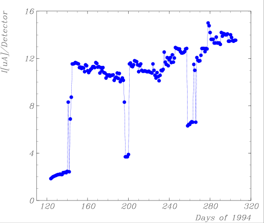
The second channel shows a faster linear increase of the reverse current and its evolution is distorted by strong jumps of the current. These jumps are abnormal, they can be explained by a local break-down of the depletion towards the border of a detector causing a short circuit in the corresponding bias-voltage-ring. The jumps provide high noise spoiling the measurement. Therefore detectors showing break-down have to be removed from the readout 444This is done by an automated procedure, ”the hot channel monitor”, which tracks the performance of each detector with time (see section 6.3).
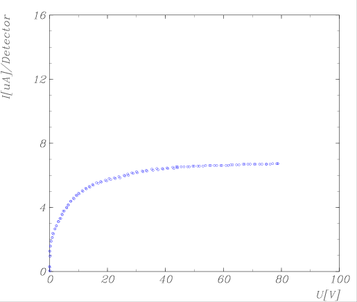
In figure 8 the I-V characteristics of the same two bias-voltage-channels are shown. The reverse current of the first channel has the typical dependence of the applied voltage. The curve shows a decreasing slope until the depletion voltage is reached (fig. 3) proving that all detectors connected to this channel are operational.
The second channel shows the normal evolution up to values of about 20 V and above this voltage the I-V characteristic is governed by an ohmic behaviour. No saturation of the current is observed indicating that at least one detector of this channel shows a break-down .
6.2 Detector Capacitance
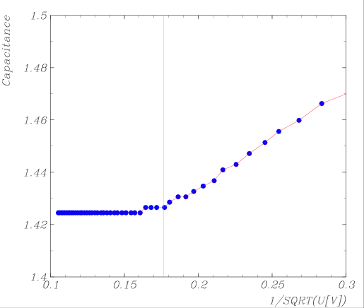
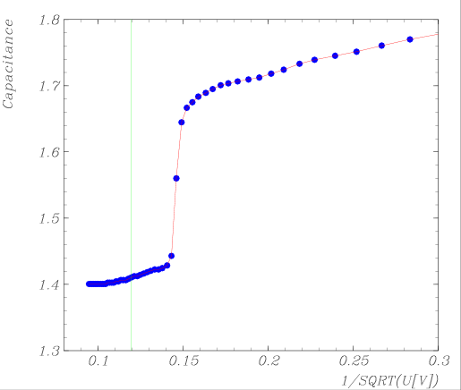
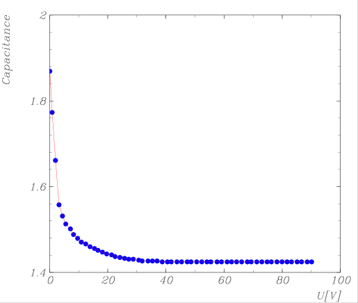
Figures 8 and 11 illustrate the C-V characteristics of two typical detectors. Figure 8 shows the C-V characteristic of a detector as a function of and figure 11 the C-V characteristic as a function of the voltage V.
The left part of fig. 8 illustrates nicely the saturation of the capacitance at depletion voltage as expected from eq.(11). The depletion voltage of the shown detector is measured to be V corresponding exactly to the value, which was determined before installation in the laboratory. The unchanged depletion voltage proves that the bulk of silicon is not damaged. The left part of fig. 11 allows to study the flat band voltage of the same detector. It is found to be 2 V. Also no change compared to the measurement made in the laboratory is observed.
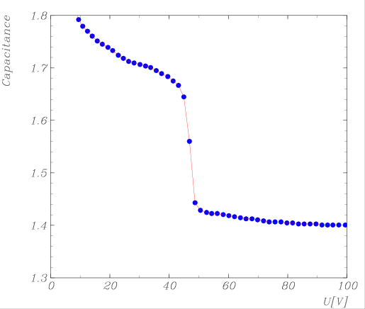
The right part of the figures 8 and 11 represent a different detector with an increased flatband voltage of V. This increase is due to radiation damage of the passivation at the border of the detector. The observed flatband voltage is lower than the depletion voltage of 82 V, still visible in the C-V characteristic.
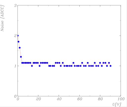
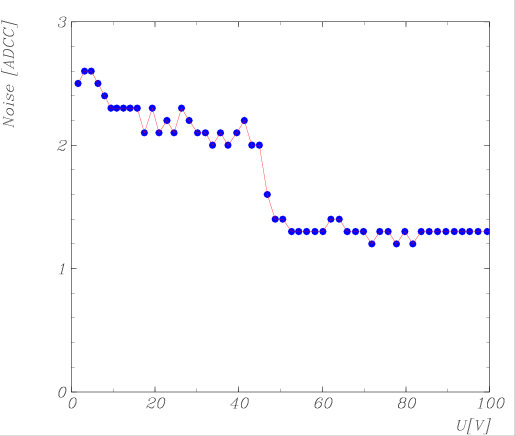
6.3 Signal Noise
The detector noise is shown in figure 11 for both of the preceding detectors as a function of the voltage . It follows for both the evolution of their C-V characteristics (see fig. 11). This is purely an effect of the used preamplifiers being sensitive to the detector capacitance, so that the detector noise itself can be neglected for undamaged detectors. The first detector has a noise of one ADC count corresponding to electrons. The noise of the second detector drops down at the voltage which corresponds to the increased flat band voltage and it also stays constant above this value.
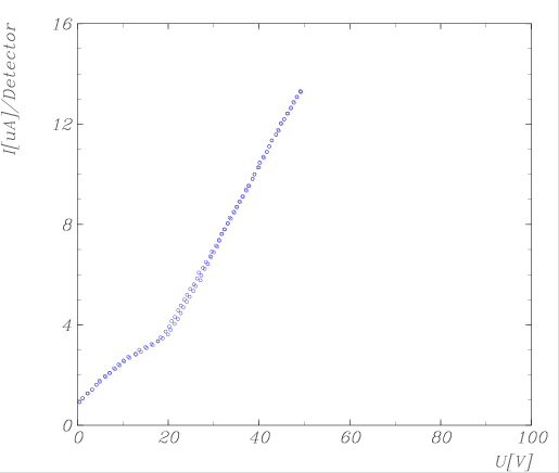
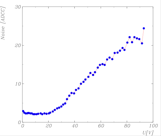
Figure 11 shows the noise performance of a detector, which is not operational due to high noise. Above 20 V indicating break-down the noise increases linearly up to 30 ADC counts ( 1GeV). This observation is in good agreement with the break-down of the I-V characteristic in figure 8. This detector has of course to be excluded from the readout in order not to spoil the energy measurement.
6.4 Absorbed Radiation Dose
The intention was to measure the integrated radiation dose produced by ionizing particles at different radial positions. Therefore several thermoluminescence dosimeters were installed inside the seventh slot of the PLUG calorimeter during the 1994 run period. The measured dose varied from 300 Gy for the inner detectors to 10 Gy for the outer ones 555During the same time the total integrated luminosity for ’94 of 4 was collected.. This measured dose is not high enough to explain the observed radiation damage. Such effects were expected at much higher dose values in the order of several kGy’s. It is therefore assumed that the used dosimeters are not sensitive to the radiation contributing most to the dose absorbed by the detectors. 666The used dosimeters RPL glastype R1T are only sensitive down to 30 keV.. Instead the major effect is most likely due to very low energetic electrons and photon from synchrotron radiation. This effect is currently being investigated in more detail [10].
7 Measurements in the Laboratory
All discussed measurements have been repeated in the laboratory after the end of the run period. This had the advantage that every single detector can be individually investigated and that no correction is needed due to the ganging of several detectors to one bias supply unit (sect. 5). The reverse current, the detector capacitance as well as the signal noise have been studied once again for each detector. The results of this final analysis of the ’94 run period are presented in the following.
7.1 Reverse Current
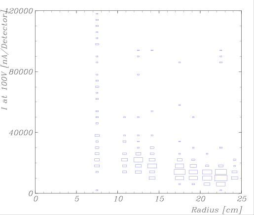
The I-V characteristic of the 648 detectors installed in the PLUG during the 94 run period has been analysed. of the detectors show a break-down as demonstrated in fig. 8 and are no longer operational anymore.
In figure 12 the correlation of the reverse current measured at 100 V and the radial position is shown for the remaining of detectors. A clear radial dependence of the increase of the reverse current is observed. The closer a detector is mounted to the beampipe the higher is its current. of the detectors have a current higher than 6 . Most of these detectors are situated in the innermost ring. In addition to the radial dependence it should be mentioned that detectors in the most backward plane where the electron beam hits first are damaged more than detectors of the front plane, through which the incoming proton beam passes first. This indicates once more that the increase of the reverse current is caused by electromagnetic radiation.
7.2 Detector Capacitance
The C-V characteristics of all detectors have been studied in the laboratory. No increase of the depletion voltage has been observed.
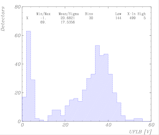
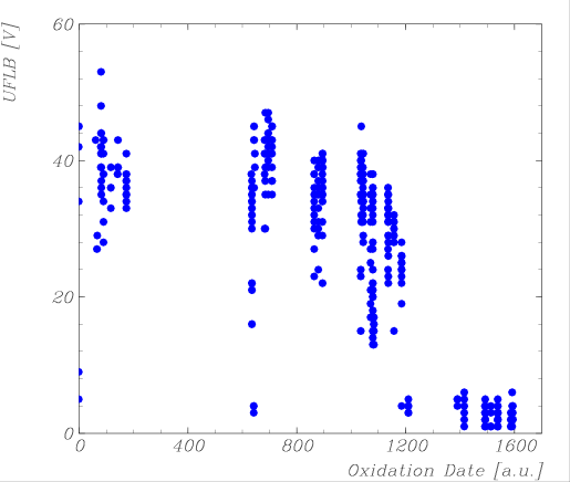
Figure 15 shows the distribution of the measured flat band voltages. Two classes of detectors are visible. The first class has an unchanged flat band voltage of about 2 V. The second class is characterized by an increased flat band voltage of arround 35 V.
Figure 15 illustrates the correlation of the flat band voltage with the oxidation date of the detector. The correlation with the oxidation date shown over the time period 1990-1993, during which the detectors were produced in different oxidation batches, proves that the newly fabricated detectors show no increase of the flat band voltage while the older ones are characterized by a saturating value of around 35 V. I
7.3 Signal Noise
8 Discussion of Results
The investigations of the reverse current, the detector capacitance and the signal noise of each detector used during the ’94 run period leads to the following observations :
The reverse current is strongly increasing with time from some 100 nA’s to several A’s per detector. The increase is highest for the innermost and most backward detectors, where the electromagnetic radiation flux impinging on the PLUG is greatest. In total of the detectors show a break-down in their I-V characteristic. These are mainly the innermost detectors exposed to the highest radiation dose. These detectors are no longer operational due to missing depletion of the silicon and must therefore be replaced for the next run period.
The detector capacitance of all detectors shows an unchanged depletion voltage, consequently radiation damage to the bulk of the silicon can be excluded. However the flat band voltage rises from 1-2 V as measured in the laboratory to a saturating voltage of around 35 V after irradiation in H1. The increase of the flat band voltage is only observed for all detectors produced before ’93, but not seen for the latest production batches.
The noise analysis reveals that detectors, which are unstable and show break-down, have high noise. Hence they have a bad signal to noise ratio and spoil the overall energy measurement of the calorimeter. Therefore, noisy detectors have to be identified as quickly as possible in order to exclude their signals from the readout. In addition detectors showing break-down affect the other detectors included in the same bias voltage channel. The fluctuating current of the bad detector leads to an equivalent fluctuation of the effective voltage for all other detectors showing up in an increased noise. To avoid this perturbation of other detectors by damaged ones it would be useful to have individual switches in order to be able to remove the bias voltage for every single detector. This is foreseen for future developments.
The main physical reason for the observed damage effect is the generation of positively charged states in the silicon oxide passivation layer (trapped charge) and the creation of defects at the interface. Both are induced by ionizing particles.
The interface states, which act as generation/recombination centers for electron hole pairs (sect. 3), are assumed to be responsible for the observed increase of the reverse current during the run period. In order to prove this assumption test detectors of much smaller size but fabricated by the same technology were irradiated in a separate laboratory experiment with 20 keV electrons. The reverse current was measured as function of dose in the range between 0.5 kGy and 5 kGy. The effect is dominated by an increase of the interface generation current with a slope of 3.6 . Using this result and taking into account the different field plate areas of the test detector and the PLUG detector a current increase of 3 as observed for the ’94 run period (fig. 8) would only be consistent with an accumulated dose in the order of 10 kGy. This large value exceeeds the results derived from the used dosimeters by a factor of about 100. As mentioned before (sect. 6.4), the dosimeters are only sensitive to ionizing radiation with energies above 30 keV. Thus we are confident that the main contribution of the radiation field causing the observed damage effects can be attributed to low energy photons respectively electrons [10].
Furthermore, the change of the flatband voltage induced by 20 keV electrons was studied for devices which were kept at zero bias or at a constant bias voltage (e.g. 80 V) during irradiation. From measurements as function of dose it was found that the increase of the flat band voltage saturates at high dose. However for a bias voltage of 80 V, which corresponds to the value typically applied to the PLUG detectors, a saturation level of 35 V is observed at 2 kGy. In contrast for irradiation at zero bias saturation occurs only above 15 kGy reaching a much lower value of 10 V. This strong effect can be explained by the different charge collection respectively trapping of electrons and holes created in the oxide layer [9],[11].
The result obtained for irradiation under bias are in accordance with those observed for PLUG detectors but an estimation of the accumulated total dose during the run period is not possible. Only a lower limit of about 2 kGy can be stated. An open question is the different behaviour of detectors from the latest production batches. They were fabricated from wafers with a different oxide and show a negligible flat band voltage shift (fig. 15, 15). So far it can be stated that the radiation hardness of silicon oxides depends strongly on the chosen technology [12].
An unambiguous and simple explanation for the observed break-down effect is difficult. One possible reason is the fact that the positive charge built up in the oxide layer especially below the field plate region at the border of the detector causes a strong increase of the electric field strength (fig. 3). Simulations of the field distribution have demonstrated that the field strength can exceed values high enough for a possible avalanche break-down [13], [14]. Inhomogeneities of the trapped oxide charge distribution may stimulate local avalanche break-down which is commonly called ”micro plasma effect”. This local effect is normally quenched by the corresponding voltage drop at the bias resistor resulting in large fluctuations of the detector leakage current as can be seen in fig. 8. Such instabilities give rise to an excessive large noise. For more detailed understanding of all damage effects described above further studies and irradiation experiments are in progress.
After the ’94 run period of the PLUG detectors were found to have been affected by radiation damage in one way or another. As a consequence it has been decided to reduce the number of active planes from eight to four for the ’95 run period thus providing the best possible signal to noise ratio. This reduction is also advantageous because it permits better monitoring of the detector characteristics by eliminating the need to gang two consecutive detectors (sect. 5). It has also been decided for the ’95 run period to minimize the time during which the bias voltage supply is activated thereby reducing sensitivity to radiation damage.
9 Conclusion
With respect to the radiation damage observed for a large amount of the silicon detectors used in the H1-PLUG calorimeter the importance and the difficulty for good monitoring of detector characteristics have been pointed out. Good monitoring permits the localisation of broken-down and noisy detectors. It is crucial for the quality of the measured data to exclude the signals of damaged detectors from the readout. It would be useful to construct the bias voltage system for future experiments in such a way, that one could switch off single damaged detectors in a voltage channel thus avoiding a degradation in performance of those detectors which are undamaged.
The observed radiation effects do not indicate a bulk damage of the used silicon detectors, but a damage to the surface caused by ionizing radiation. This result is unexpected. In particular a low radiation hardness of the border of the used detectors forming a MOS-structure is found, which is observed by an unexpectedly high increase of the flat band voltage. The possible effects of radiation damage to the surface of silicon detectors, which will be predominantly used by the future LHC experiments, have not been systematically investigated especially in correlation with the applied process technology. Given the results presented in this paper the importance of such investigations into surface radiation damage is stressed.
Acknowledgements
We greatly benefited from the help of G.Lindstroem, E.Fretwurst, H.Jarck and from the proofreading of this paper by G.Lopez. We would like to thank H.Krueger 777Student, Universität Heidelberg, supported by the DESY Summer Student Program for his collaboration during the summer ’94. Financial support is acknowledged from the BMFT under contract 056HH17P.
References
- [1] ATLAS Collaboration,” Letter of intent for a general purpose P-P experiment at the large hadron collider at CERN”,CERN-LHCC-92-4, Oct 1992. 108pp
- [2] RD2 Collaboration,”Progress Report on the RD2 Project”,CERN/DRDC94-34, Aug. 1994
- [3] RD20 Collaboration,”Development of high resolution silicon strip detectors for experiments at high luminosity at LHC”,RD20/Status Report, CERN/DRDC94-39, Oct. 1994
- [4] H1 Collaboration,”The H1 detector at HERA”,DESY-93-103,July 1993
- [5] H1 Collaboration,”First measurement of the deep-inelastic structure of proton diffraction”,Phys. Lett. B 348 (1995) 681-696
- [6] W. Hildesheim, V. Riech, M.Seidel,”The Plug Calorimeter Users Guide”, Internal Report H1–08/94–372
- [7] E. Fretwurst, H. Herdan, G. Lindström, U. Pein, M. Rollwagen, H. Schatz, P. Thomsen, R. Wunstorf,”Silicon Detector Developments for Calorimetry: Technology and Radiation Damage”, Nucl.Instr.& Meth. A288(1990) 1-12
- [8] T. Schulz,”Untersuchung zur Strahlenschädigung von Silizium Oberflächensperrschicht Detektoren durch 1,8 MeV Elektronen”, Diploma thesis, Hamburg 1991
- [9] P. Schlichthärle,”Untersuchung von Oberflächeneffekten in Silizium-Detektoren nach Schädigung mit 20 KeV Elektronen”, Diploma thesis, Hamburg 1995
- [10] M.Buck,”Monte Carlo Simulation niederenergetischer elektromagnetischer Strahlung in Silizium-Detektoren”,Diploma thesis in preparation, Hamburg 1995
- [11] D. Bräunig,”Wirkung hochenergetischer Strahlung auf Halbleiterbauelemente”, Springer-Verlag, 1989
- [12] A.B.D. Roderick,”The structure of , its defects and radiation hardness”, IEEE, Trans. Nucl. Sci. NS 41, No.3 (1994) 452
- [13] R.H. Richter,MPI-Halbleiterlabor, Muenchen, private communication
- [14] H.W. Kraner, Brookhaven National Laboratory, Instrumentation Division, USA, private communication