KEK Preptint 93-43
June 1993
![[Uncaptioned image]](/html/hep-ex/9412007/assets/x1.png)
Test of Various Photocathodes
***
published in Nucl. Instrm. Meth. A 343 (1994) 117.
Ryoji Enomoto, Takayuki Sumiyoshi
National Laboratory for High Energy Physics,
1-1 Oho, Tsukuba-shi, Ibaraki 305, Japan
and Yoshio Fujita
Hamamatsu Photonics K. K.,
314-5 Shimokanzo, Toyooka Vill., Iwata-gun, Shizuoka 438-01, Japan
Abstract
A test of various photocathodes was carried out. The tested materials were CsI, CsTe, their multi-layers and so on. The quantum efficiencies of the various materials were measured under a vacuum and/or after exposure to several kinds of gases.
1 Introduction
Various attempts to understand the CP violation mechanism[1] are presently being planned. mesons seem to be a most promising probes to be investigated[2]. In order to carry out such investigations, B-factory projects have been proposed[3]. One of them is the KEK B-factory project, in which asymmetric double storage rings to produce high-rate moving-s will be constructed[4]. To measure CP asymmetry, we need to identify the b-flavor: in other words either or . The best probes have been found to be charged mesons from the cascade decays of mesons[5]. / separations in the momentum range between 0.5-4 GeV are required.
In addition, a fast response of the detector is required, due to the use of a high-luminosity accelerator. We have adopted a fast ring imaging Cerenkov detector (in short, “fast RICH”[6]) for / identification. Solid photocathodes which can be operated even after exposure to air have recently been discovered; they were also proven to be useful in a fast RICH[7]. The most stable (to air-exposure) photocathode was found to be CsI coated with a thin layer of TMAE. However, the quantum efficiencies have not yet been established in the presence of air or MWPC-gases[8].
We have systematically carried out measurements of the quantum efficiencies of CsI as well as other materials. The optimization of a CsI photocathode and the search for other materials have been carried out.
2 Test Setup
In order to measure the quantum efficiencies of various photo-sensitive materials, we have adopted a phototube technique. A test phototube (diode) is shown in Fig 1.
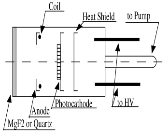
Window were made of or quartz. The cathode was made of an Al-plated-Ni electrode, and various photo-sensitive materials were plated on it. Tests were then carried out at room temperature. The spectral responses were measured using monochrometers.
3 Test on a Single Material in a Vacuum
3.1 CsI
At first, we optimized the thickness of the CsI photocathode. The quantum efficiencies were simultaneously monitored at a wavelength of 170 nm with vacuum-plating CsI. The result is shown in Fig 2.
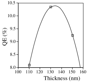
The real thickness of the CsI photocathode was calibrated, and the correction factor was typically 30%. We therefore concluded that the optimized thickness was approximately 130 nm. This value is different from that of reference [7] about a factor of 4. A factor of 2 can be explained by reflection at the Al-surface of the electrode. There may be a systematic difference in the CsI quantum efficiency due to such circumstances as gas. Our measurement was carried out under a vacuum. We replaced the cathode-electrode with an stainless steel which has a higher reflectivity, however, the quantum efficiency was the same.
The spectral response of the quantum efficiency is shown in Fig 3.
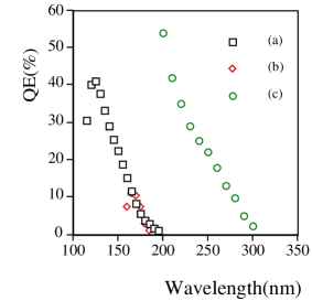
The points indicated by (a) were measured using a window and by (b) a quartz window. The peak is located at 120 nm (QE=40%), where cutoff is 115 nm.
3.2 CsTe
The CsTe photocathode has been known to be sensitive at longer wavelengths and to have a higher QE than that of CsI. This photocathode was tested with a quartz window phototube. Although the optimized thickness was located at around 100-300 nm, this requires more study. The quantum efficiency was plotted with the points indicated by (c) in Fig 3. A QE of 55% was obtained at 200 nm.
3.3 CsI(Tl)
We next tested a Tl-doped CsI in order to find any difference in the spectral response. After that, windows were used in the test phototubes. The measurements were carried out at the optimized thickness. The measured quantum efficiency is shown in Fig 4.
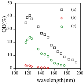
We did not observe any spectral differences, compared with those found in the pure CsI. This photocathode was thus also proven to be stable.
3.4 NaI(Tl)
NaI is known to have a lower work function (Eg), and slightly higher electron affinity (Ea). We anticipate the shift of the sensitivity at the longer wavelength region. The result is shown in Fig 4. Unfortunately, the quantum efficiency is too low to be used in our case.
3.5 KI
KI has a similar Eg and Ea compared to that of NaI. The result is shown in Fig 4. A quantum efficiency of 24% at 120 nm was obtained. However, the sensitivity in the longer wavelength region was significantly lower than that of CsI. There is no effective sensitivity with a quartz window.
4 Quantum efficiency after gas exposure
In this chapter we report on the sensitivity changes occurring after exposing photosensitive materials to various gases.
4.1 CsI
At first we tried . After 1 hour of exposure to , the quantum efficiency was reduced by about 5%. In these measurements, the thickness of CsI was 130 nm. The dependence on the thickness will be measured in the near future. We next tried , and a 50% reduction of the quantum efficiency was observed. was also tried. The sensitivity was found to be stable against exposure. CsI was found to be stable against amin-gas.
We finally we tried air exposure. The result is shown in Fig 5.
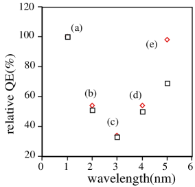
We monitored the anode current at two wavelengths of light sources (121.6 and 160.8 nm). There were 5 steps: (a) before exposure, (b) after 1 hour of exposure, (c) 2 hours, (d) 3 hours, and (e) leaving the test photocathode for 5 days in vacuum after (d). Although the quantum efficiencies were reduced by the exposures, they recovered after more than 20 hours of vacuum pumping.
We tried yet another test. There was one exposure of 4 hours; after that, the test photocathode was left in a vacuum. The results are shown in Fig 6.
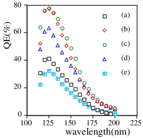
There was a drastic change in the sensitivity. The quantum efficiency became as high as 77% at 120 nm (before exposure, it was only 40%). However, it was not stable after the vacuum-pumping. There was a possibility that some contamination in the air contributed to the increase in the quantum efficiencies of CsI. We need to carry out a more systematic check of this effect.
4.2 CsTe
CsTe showed a similar result compared to that of CsI regarding exposure. A 5% reduction of the quantum efficiency was observed. Air exposure was serious, and the quantum efficiency dropped to less than 1%.
5 Double-layer photocathodes
CsI was proven to be stable against air exposure. We thus tried to coat an unstable material with CsI (a double photocathode).
5.1 CsTe + CsI
The most promising UV photocathode was CsTe. It has a higher sensitivity at wavelengths greater than 200 nm. The advantage involves the use of a quartz window. We tried to coat CsTe with CsI. Unfortunately the result was negative. After plating a thin film of CsI, CsTe itself reacted with CsI and the quantum efficiency dropped rapidly, even in a vacuum. After air exposure, additional damage was observed.
5.2 CsSb + CsI
CsSb was known to match CsI in a vacuum, and it shows a good sensitivity to visible light. We tried to coat a CsSb photocathode with CsI [9]. At first in vacuum, the coating was carried out by a few nm steps. After each step, the quantum efficiency was observed to be reduced by 10-20%. After 6 steps, we exposed it to air and then measured the quantum efficiency. It had become reduced by one order (i.e., less than 1%). We therefore concluded that we cannot prevent a reaction with air by using a thin film of CsI.
5.3 CsI + NaI
NaI was stable in air. We thus tried to coat NaI with CsI and CsI with NaI. This was a miscellaneous test in order to understand any changes in the quantum efficiencies by a coating procedure. In the first case, the quantum efficiency at 170 nm was the same as that of pure CsI, and that at 180 nm was half. In the latter case, however, the quantum efficiency at 170 nm was half and at 180 nm it was 1/4. There was a reduction by the double-layer technique.
6 Conclusion
We tested various photocathodes for gas-filled photon detectors, such as a ring-imaging Cerenkov detector using test phototubes. Various materials which were stable to air exposure were tested. Among them, CsI was found to be the most suitable, and various optimizations were carried out. Other attempts, such as using new materials other than CsI, or using double-layer photocathodes did not show any stable results.
Acknowledgement
We thank a discussion with Prof. T. Ypsilantis (College de France). We appreciate the support given by Prof. F. Takasaki in carrying out this R and D. This work was carried out under collaboration with Hamamatsu Photonics K. K. (HPKK). Especially, the work by Mr. T. Hakamada, Mr. S. Suzuki, and Mr. Y. Hotta is acknowledged.
REFERENCES:
[1] M. Kobayashi and T. Maskawa, Prog. Theor. Phys., 49 (1973)
652.
[2] I. I. Bigi and A. I. Sanda, Nucl. Phys. B193,
(1981) 85.
[3] P. J. Oddone, private communication.
[4] KEK B-factory Task Force, KEK report 90-23, unpublished.
[5] R. Aleksan et. al., Phys. Rev. D39 (1989) 1283.
[6] R. Arnold et. al., Nucl. Instrum. Methods, A314 (1990) 465.
[7] J. Seguinot et. al., Nucl. Instrum. Methods, A297 (1990) 133.
[8] B. Howeneisen et. al., Nucl. Instrum. Methods, A302 (1991) 447.
[9] suggested by T. Ypsilantis (College de France).