CALICE ELECTROMAGNETIC CALORIMETER READOUT STATUS
The status of the prototype readout boards for the CALICE electromagnetic calorimeter is presented. Results on linearity, noise, and minimum ionising signals, both from a radiactive source and cosmic rays, are shown.
1 Introduction
The CALICE Electromagnetic CALorimeter (ECAL) will be a silicon-tungsten sampling calorimeter [1] with 30 layers of silicon wafers, each containing an array of diode pads, giving 9720 channels to be read out. The signal from each pad is amplified by a Very Front End (VFE) ASIC [2] which multiplexes the signals from 18 pads onto one output line. The silicon wafers and VFE chips are mounted on VFE PCBs [3], each containing up to 12 VFE ASICs, equivalent to 216 pads. The signal cables from the VFE PCBs connect directly to the readout boards and the latter are the subject of this paper.
2 The Readout Board Design
The CALICE ECAL Readout Cards (CERC) [4] are 9U, double-sided, VME boards originally based on the CMS silicon tracker Front End Driver board [5]. They contain 16-bit ADCs for each VFE ASIC output and 16-bit DACs for calibration. The 16-bit ADCs can operate at up to 500 kHz and so take around 80 s to read out all 18 multiplexed channels from a VFE ASIC. There is no data reduction on the CERCs; all signals from all channels will be read out and this corresponds to 5 kBytes per CERC per event, or 30 kBytes total per event. These data are stored in an on-board 8 MByte memory, which allows over a thousand events to be buffered during a spill before readout via VME.
An overview of the CERC is shown in figure 1.
 |
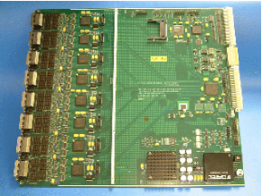 |
Eight Front End (FE) FPGAs control all signals on the front panel connectors to and from the VFE PCBs. The Back End (BE) FPGA gathers and buffers all the event data from the FEs and provides the VME interface. Trigger logic is implemented in the BE FPGA, for which the logic is only active on one board. A total of six CERCs will be needed for the entire ECAL readout. The prototype design of the CERCs was completed in summer 2003 and two prototype CERCs were fabricated in November 2003. A photograph of one of these prototypes is also shown in figure 1.
The CERC prototypes have been extensively tested with a prototype VFE PCB containing one cm2 silicon wafer. Not all the final firmware for the FE and BE FPGAs is yet complete; in particular, the complex data path from the FEs to the 8 MByte memory via the BE and then to the VME interface is not functional. Hence, these tests have been done using a simple RS232 interface directly from the FEs to a PC. This gives a slow rate of around 1 Hz for readout (compared with an expected rate of around 1 kHz for the final system) but this is sufficient for this round of tests. In particular, the analogue parts (the ADC and DAC operation) are operated in the same way as for the final system, so results from these tests give an accurate indication of the performance of these sections of the CERC.
3 Internal Loopback Tests
In these tests, the DAC output was looped back directly to the ADC inputs. This allowed a straightforward linearity scan of the system independent of the VFE PCBs. A simple straight-line fit gives residuals of around 1-2 ADC counts, corresponding to an intrinsic linearity of 0.01%. The gains, measured from the slope of the ADC vs DAC response, show a spread of around 1%. The noise is around 1 ADC count for all channels. The DAC was seen to saturate in the first 1% of its range; this effect is understood and can be corrected in the production version.
4 Strontium Source Tests
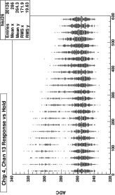
A 90Sr beta source was used to give a relatively high rate of signals in the wafers so as to determine the required timing. The VFE sample-and-hold needs to be timed so as to capture the peak of the CR-RC shape. This offset is software configurable in steps of 6.25ns. The signal due to the 90Sr as a function of the timing offset is shown in figure 2. The separation of the signal (at around 300 counts) from the pedestal (at around 255 counts) is clearly seen for small offsets, while the two merge together as the offset increases. The offset was set to maximise the separation of the signal from the pedestal.
5 Cosmic Tests
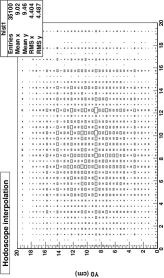
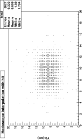
A hodoscope scintillator cosmic ray telescope built at Ecole Polytechnique [3] was used to observe cosmic ray tracks in the wafer. The tracks determined from hodoscope information were interpolated into the plane of the wafer and the distribution of these positions in the plane is shown in figure 3. The same distribution after requiring any wafer pad to have a signal at least 40 ADC counts above pedestal is also shown in figure 3, clearly indicating the outline of the wafer in the hodoscope.
|
|
Pads consistent with the interpolated hodoscope track were used to determine the cosmic signal size. The distribution of ADC values relative to the pedestal for these pads is shown in figure 4.
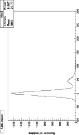
The clear peak at around 45 ADC counts gives the average signal value of a minimum ionising particle (MIP). This means the full ADC range corresponds to around 700 MIPs, which is sufficient for the CALICE beam test studies. In addition, the MIP/noise value is around 5/1, above the requirement of 4/1. Hence, the system satisfies the basic requirements for CALICE.
6 Future Plans
Tests will continue over the summer with production of the CERCs scheduled for early autumn. These will be used for a first beam test of the whole ECAL at DESY in a 6 GeV electron beam and this is scheduled for late 2004 and early 2005. Following this, further beam tests using hadrons are foreseen, where the ECAL will be tested together with several hadron calorimeters. These should continue throughout 2005 and into 2006.
References
References
- [1] polywww.in2p3.fr/flc/calice.html.
- [2] J. Fleury, these proceedings.
- [3] J.-C. Vanel, these proceedings.
- [4] www.hep.ph.ic.ac.uk/calice/electronics/electronics.html.
- [5] www.te.rl.ac.uk/esdg/cms-fed/fed_final_home.html.