Test Beam Results of ATLAS Pixel Sensors
Tommaso Lari
INFN, Sezione di Milano, Via Celoria 16, I-20133 Milano, ITALY
On behalf of the ATLAS Pixel Collaboration
Abstract
Silicon pixel detectors produced according to the ATLAS Pixel Detector design were tested in a beam at CERN in the framework of the ATLAS collaboration. The detectors used n+/n sensors with oxygenated silicon substrates. The experimental behaviour of the detectors after irradiation to and 600 kGy is discussed. At the sensor bias voltage of 600 V the depleted depth is measured to be 229 m, the mean collected charge is 20000 electrons, the detection efficiency is 98.2% and the spatial resolution is 9.6 m.
1 Introduction
At the LHC silicon microstrip and pixel detectors will be exposed to unprecedented levels of ionizing and hadronic radiation. As a consequence of displacement damage arising from hadronic radiation, the silicon detectors will change their characteristics during their lifetime [1, 2]. Potential radiation-induced performance degradation is a serious issue, which has been studied in detail.
The ATLAS Pixel Detector [3, 4] is required to be tolerant to an hadronic fluence 111In this paper the fluences are converted in where is the number of particles with the non-ionizing energy loss of a 1 MeV neutron. of and an ionizing dose of 550 kGy. In order to verify their ability to meet these requirements, some pixel detectors produced according to the ATLAS design have been exposed to 110% of the target fluence and dose and have been operated in a test-beam experiment at CERN. Measurements of the thickness of the depleted region, of the efficiency and uniformity of charge collection, of hit detection efficiency and spatial resolution have been performed and are reported here.
2 Tested devices and experimental setup
The ATLAS Pixel sensors [5] consist of implants on a high resistivity n-bulk substrate. This choice allows the detector to be operated in partial depletion mode after type inversion due to irradiation, as the n-p junction and the depleted zone are located near the pixels. The substrate is oxygenated to improve its radiation hardness.
The pixel dimensions are and the sensor thickness is 250 m. The isolation between pixels is achieved with the p-spray technique [5, 6]. A network of bus lines, one every other column pair of pixels, is connected to an implant dot near each pixel. This bias grid allows to bias the detector during testing, before attachment of the front-end electronics.
The irradiated devices had a sensor connected to a front-end electronics chip [7, 8, 9] of the same size. In ATLAS, pixel sensors will have a size of and will be connected to 16 front-end chips.
Every pixel cell in the sensor is connected via bump-bonding[3] to a matching cell in the front-end chip, which includes a charge preamplifier and a discriminator. The pulse height is obtained from the time the signal stays over the discriminator threshold. The Time-Over-Threshold (ToT) is calibrated [9] for each pixel by injecting a known charge, with an accuracy of about 10%. During test-beam operation the pixel thresholds had a mean value of 3000 electrons with a dispersion of 300 electrons rms. The noise was 400 electrons.
Irradiation was performed after bump-bonding at the CERN PS with a beam of 20 GeV protons [10]. The detectors received the total ionizing dose of 600 kGy, corresponding to a fluence of .
The test beam was performed at the CERN SPS accelerator with a pion beam of 180 GeV/ momentum. A beam telescope [11] consisting of 4 pairs of double-sided silicon microstrip modules was used to track the particles. The position resolution of tracks projected onto the devices under test was 6 m.
During irradiation, between irradiation and the test beam operation and during the test beam operation the devices were kept below 0 0C, suppressing the time dependence of defect concentration in the silicon. At the LHC, the cumulative effect of defect annealing after 10 years of operation is predicted to reduce the initial concentration of defects, so that the results presented here are conservative.
3 Thickness of depletion zone
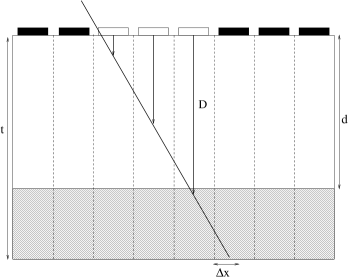
The measurement of the depletion zone depth is performed with data taken with particle beam incident on the sensor at an angle of 300 respect to the normal to the pixel plane (Fig. 1), as described in [12, 13]. A particle crossing the detector produces a cluster of hits consisting of the pixel cells that collect a significant fraction of the charge released in the subtended segment of the track. To measure the depth of the depleted region the maximum depth of track segment was used (Fig. 1); it was defined as the distance of the center of the track-segment subtended by a given pixel from the pixel itself. Since the entrance points of the tracks are uniformly distributed, all of the depths vary continuously and the maximum observed depth is a measurement of the depletion depth within the detector.
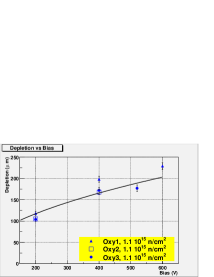
In Fig. 2 the depletion depth measurements of the irradiated sensors are plotted as a function of the applied bias voltage. The three different symbols refer to three sensors irradiated to the same fluence. The continuous line is the prediction based on the model [1] for the depletion depth of oxygenated sensors irradiated to before annealing, assuming a uniform space charge, so that the depletion depth scales as the square root of the bias voltage. The measured depletion depth is in good agreement with this assumption. At 600 V, which is the maximum bias voltage foreseen in ATLAS, the sensors are almost fully depleted.
4 Charge collection efficiency and uniformity
The sum of the charges collected by the pixels in a cluster (cluster charge) provides a measurement of the charge collection efficiency of the sensor.
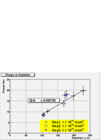
In Fig. 3 the average cluster charge at normal incidence is plotted against the depletion depth. As expected, the two quantities are proportional. At 600 V an average signal of 20000 electron is seen, to be compared with 25000 electrons collected by not irradiated and fully depleted sensors. Both numbers are affected by the 10% uncertainty on the absolute scale provided by charge calibrations. The ratio between charge and depletion depth, coming from the fit to the data is m.
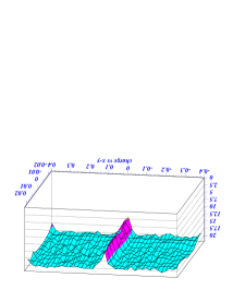
The charge collection uniformity have been studied by considering the mean cluster charge as a function of the impact point of traversing particles relative to the center of a pair of pixel cells (Fig. 4) as done in [14] The coordinate axes are parallel to the short (50 m) and long (400 m) edges of the pixels, respectively, and are centered in at the centre of a single pixel and in between two adjacent pixels belonging to a column pair.
The uniformity is pretty good, except in the region between two columns where the bias grid is located (). Here a significantly reduced signal is observed. No loss is observed between pixel columns where the bias grid is not present ( mm) or between pixel rows.
5 Detection efficiency
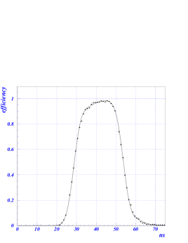
At the LHC the pixel detectors will be required to identify the bunch crossing which has produced a particle with an efficiency in excess of 97%. As the LHC bunch crossing rate is 40 MHz, the charge collected by pixel must be detected in a time window of 25 ns.
Since the extracted beams used at CERN did not have an RF structure and the readout electronics was operated with a 40 MHz asynchronous clock (with respect to the particles), the phase between the arrival time of every particle and the clock was measured. During operation at the LHC this phase can be set for each individual module. Further, for an accepted trigger of beam particle the pixel hits belonging to 16 contiguous “bunch crossings” (clock periods) were read out. This allowed to study the timing behaviour of the detectors [15, 16].
In Fig. 5 the detection efficiency is plotted against the difference between the beam trigger and the beginning of the clock period in which hits are looked for. The maximum efficiency is 98.2% which is well within the Pixel Detector requirements.
6 Spatial resolution
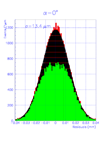
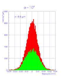
Spatial resolution is a key feature of the Pixel Detector, which strongly affects the vertex-finding performances of ATLAS. If there is no charge sharing between pixels, the hit position is reconstructed as the centre of the fired pixel, and the resolution is related to the pixel pitch by . If the charge released by the particle is shared by adjacent pixels, charge interpolation is possible, leading to improved resolution. The amount of charge sharing depends on the particle incidence angle, the thickness of depleted zone and the charge collection performances.
In what follows, resolution along the short (50 m) pixel direction will be considered.
In Fig. 6 the distribution of the residuals between the hit position measured by the pixel detector and the track position provided by the beam telescope is shown for normal incidence and an incidence angle of . The latter was chosen to be representative of ATLAS tracking conditions [17]. The lighter histograms represent the one-pixel cluster residuals, the darker ones include all clusters. The resolution is worse at normal incidence because of the larger fraction of one-pixel clusters, for which no charge interpolation is possible. A gaussian fit to the residuals distribution yields m at normal incidence and m at incidence angle.
7 Conclusions
ATLAS Pixel detectors with oxygenated silicon sensors and rad-hard electronics have been irradiated to fluence and 600 kGy dose, 10% more than the design values. They have been tested in a beam and were found to meet all ATLAS specifications. The thickness of the depletion zone was found to be m at 600 V of reverse bias voltage. The mean signal height was % electrons, to be compared with % electrons before irradiation. The hit detection efficiency in a time window of 25 ns was 98.2% and the spatial resolution at 100 incidence angle was 9.6 m.
Acknowledgements
The work reported here represents the joint effort of many individuals in the ATLAS Pixel collaboration. I would like to thank all of them, in particular John Richardson and Kevin Einsweiler from LBNL, Berkeley, and Attilio Andreazza, Francesco Ragusa and Clara Troncon from the Milan ATLAS group.
References
- [1] G. Lindström et al. [ROSE Collaboration], Nucl. Instrum. Meth. A 466, 308 (2001).
- [2] Z. Li, presentation given at Pixel 2002 conference (2002), in these proceedings.
- [3] The ATLAS Pixel collaboration, ATLAS Pixel Detector Technical Design report, CERN/LHCC-98-13 (CERN 1998).
- [4] M. Garcia-Sciveres, presentation given at Pixel 2002 conference (2002), in these proceedings.
-
[5]
M. S. Alam et al.,
Nucl. Instrum. Meth. A 456, 217 (2001).
I. Gorelov et al., Electrical characteristics of silicon pixel sensors, ATL-INDET-2001-011 (2001), to be published in Nucl. Instr. and Meth., sec. A. - [6] R. H. Richter et al., Nucl. Instrum. Meth. A 377, 412 (1996).
- [7] K. Einsweiler, presentation given at Pixel 2002 conference (2002), in these proceedings.
- [8] R. Beccherle, presentation given at Pixel 2002 conference (2002), in these proceedings.
- [9] J. Richardson, presentation given at Pixel 2002 conference (2002), in these proceedings.
- [10] A. Saavedra, presentation given at Pixel 2002 conference (2002), in these proceedings.
- [11] J. Treis, P. Fischer, L. Klingbeil, H. Krueger, N. Wermes and T. Lari, Nucl. Instrum. Meth. A 490, 112 (2002) [arXiv:physics/0210004].
- [12] I. Gorelov et al., Nucl. Instrum. Meth. A 481, 204 (2002).
- [13] T. Lari and F. d. Ragusa, CERN-THESIS-2001-028.
- [14] C. Troncon, IEEE Trans. Nucl. Sci. 47, 737 (2000).
- [15] F. Ragusa, Nucl. Instrum. Meth. A 447, 184 (2000).
- [16] A. Andreazza, Performance of the Atlas Pixel Detector Prototype Modules, to be published in the proceedings of the 6th international conference on position sensitive detectors (Leicester, 2002).
- [17] T. Lari, CERN/ATL-INDET-2001-004 (2001).