Readout Concepts for DEPFET Pixel Arrays
Abstract
Field effect transistors embedded into a depleted silicon bulk (DEPFETs) can be used as the first amplifying element
for the detection of small signal charges deposited in the bulk by ionizing particles, X-ray photons or visible light.
Very good noise performance at room temperature due to the low capacitance of the collecting electrode has been
demonstrated. Regular two dimensional arrangements of DEPFETs can be read out by turning on individual rows and reading
currents or voltages in the columns. Such arrangements allow the fast, low power readout of larger arrays with the
possibility of random access to selected pixels. In this paper, different readout concepts are discussed as they are
required for arrays with incomplete or complete clear and for readout at the source or the drain. Examples of VLSI
chips for the steering of the gate and clear rows and for reading out the columns are presented.
Keywords: DEPFET, monolithic active pixel sensors, integrated amplification, readout electronics
PACS: 06.30.Bp, 07.50.Ek, 29.40.Gx, 87.58.Mj, 87.59.Bh
1 Introduction
Silicon sensors are widely used for the detection of visible photons, soft x-rays and ionizing particles in many industrial and medical applications as well as in particle physics. An important figure of merit is the noise of the sensor. It should be as low as possible to improve the spectroscopic performance, to increase the spatial resolution and to be able to detect low charge depositions for instance from low energetic -rays (e.g. ) or from minimum ionizing particles in thin sensors () as they are required in the innermost layers of vertex detectors for particle physics [1]. A very low noise of rms has been demonstrated [2] with single DEPFET devices which integrate a p-channel field effect transistor into a fully depleted bulk [3]. Electron-hole pairs generated by photon absorption or by ionizing radiation are separated in the electric field of a sidewards-depleted bulk. The electrons drift to a region under the transistor channel, the internal gate, where they modulate the drain current of the FET according to for small charges. In addition to the modulation through the internal gate, the drain current can be switched off by a positive potential at the external gate. This makes it possible to arrange several square, rectangular or hexagonal DEPFET devices in an array made out of columns and rows as explained in the next section.
The charges accumulated in the internal gate remain in the local potential minimum so that multiple non-destructive readout is possible. They must be removed regularly to avoid saturation and to prepare a well defined initial condition. The clearing of charges from the internal gate can be achieved with positive signals on separate clear contacts. The design of these structures is difficult because no charges should be lost into the clear contacts in normal operation mode while all charges should be removed from the internal gate while clearing. A complete clearing could not be achieved on existing DEPFET devices even with voltages of up to so that the fill state of the internal gate has to be measured and memorized after the clear pulse by suited readout electronics. A new generation of DEPFET devices [4] should provide a complete clear so that different readout concepts become possible.
After an introduction of the matrix arrangement and the time sequence of the readout, we describe existing readout electronics for devices with incomplete clear. We then propose a concept for the fast drain readout of devices with complete clear.
2 Readout of DEPFET arrays
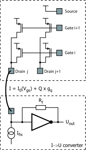
The arrangement of many DEPFET devices in a two dimensional array is schematically shown in Fig. 1 for the case of a current readout at the drain. The external gates and the clear contacts (not shown for simplicity) are connected horizontally in rows while the drains are connected in columns. The drain current in all devices except in one row is switched off by applying a positive voltage to the external gates. The external gates of the p-channel DEPFETs in the active row are connected to a more negative voltage to enable a current flow in the drain. This current, which is accessible at the column contacts, depends on and on the charge accumulated in the internal gate. Any noise on the external gate is amplified by the transconductance of the transistor so that a low noise voltage source is required. This problem is avoided by connecting the gate row directly to source potential so that . The drain current is then mainly determined by the geometry and doping profiles of the DEPFET devices. The drain current is often converted to a voltage for instance with the simple converter sketched in Fig. 1. The offset current , which is not carrying any information, can be subtracted immediately by a constant current source so that the dynamic range of the converter is not wasted.
2.1 Readout sequences for incomplete and complete clear
The switching sequence of the various gate and clear rows and the processing of the currents at the bottom of the columns depends very much on the characteristics of the clearing procedure.
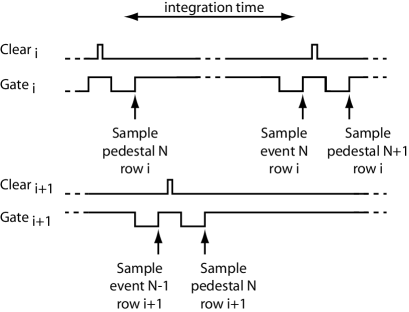
For devices with incomplete clear, the charge left in the internal gates must be determined after every clear pulse by turning on the row as indicated in Fig. 2. The row is then re-measured after the frame interval. The charge accumulated during the integration time in the internal gate is calculated as the difference of these two drain currents divided by the of the device. The other rows must be processed between the pedestal- and the signal measurement so that many different currents are present in a column before the signal measurement can be done. The pedestal values of the complete array must therefore be memorized during the frame interval with an absolute precision of less than the targeted pixel noise. The required relative precision is very high due to the large standing pedestal current in the DEPFET device. For a current of and devices with for instance, a relative precision of is required for a fluctuation of . Note that this requirement concerns mainly the noise introduced in the sampling procedure while systematic errors (for instance due to charge injection) cancel out in the subtraction. The requirement can be relaxed by an order of magnitude if a large fraction () of the pedestal current is subtracted with a low noise current source prior to the conversion as shown in Fig. 1. The temporary storage of the pedestal values could be done on a readout chip at the bottom of small arrays, but it is not feasible for large structures. The data must therefore be processed by the full readout system which must provide a large dynamic range to cope with fluctuations of the standing drain current in the order of for existing arrays.
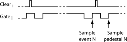
For devices with complete clear, a unique pedestal value per pixel measured just after the clear pulses for instance at the beginning of the run could be used. This approach would, however, still require the measurements of large signals and an ’off-line’ subtraction. The readout sequence shown in Fig. 3 avoids this by comparing the signal current with the pedestal value after the next clear pulse. Note that this is only possible because the complete clearing leaves the internal gate in the same well defined (empty) state. Because signal and pedestal measurements are following each other immediately, the subtraction can be easily done on the readout chip and no long time storage of large signals with high precision is required. The noise performance could be degraded in this scheme if the clear pulse introduces additional noise contributions, for instance by changing the state of traps in the transistor channel. This must be further studied in the future.
2.2 Drain and source readout
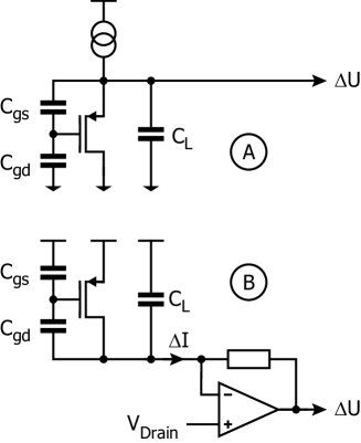
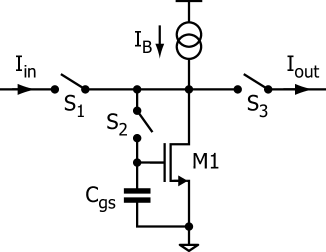
The vertical busses of the array can be connected to the drains or to the sources of the individual DEPFET devices. In the practical design of the array, however, other considerations can impose one or the other type of readout. (If the vertical bus is, for instance, implemented by connecting the outer implants of the individual DEPFETs, the more negative potential must be used there to push the electrons towards the internal gate at the inside of the annular structure. The bus must therefore be connected to the drains in this case.) The two readout types are sketched in the simplifying schematic of Fig. 4 which shows the DEPFET together with the parasitic capacitances from drain and source to the internal gate.
For readout at the source (Fig. 4A), a current is forced through the device by an external current source. The voltage change at the source in this follower configuration is measured. It is given approximatively by [5]
| (1) |
as long as the transconductance of the device is large. does not play a role in this expression because remains constant due to the unity gain of the arrangement. The rise time of the voltage signal is severely degraded by the bus capacitance which must be charged by the current change in the DEPFET. This current change is small, however, due to being nearly constant. One finds [5]
| (2) |
This settling time constant can easily reach several microseconds so that the source follower readout is not suited for very high speed applications.
For readout at the drain, the charge in the internal gate leads to a current change which can be converted to a voltage by a simple converter as indicated in Fig. 4B. The converter can hold the bus at a constant potential so that the bus capacitance does not affect the speed anymore. The gain is given by
| (3) |
A drawback of this readout scheme is the sensitivity to fluctuations in the device threshold and to voltage drops on the source traces which are amplified by the DEPFET so that fairly large current fluctuations from pixel to pixel must be coped with.
3 Examples of chips for steering and readout
The central elements of several different chips suited for the readout of DEPFET arrays are presented in this section. As discussed above, a distinction between readout at source/drain and for devices with complete/incomplete clearing of the internal gate can be made.
3.1 Control of gate and clear voltages
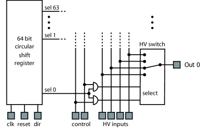
The gates of the DEPFET rows must be activated consecutively during the readout cycle. Furthermore, the row-wise clear signals and, in more advanced DEPFET structures, a clear-control signal must be driven. The voltage swings of these signals of up to exceed the supply voltages of ’standard’ CMOS technologies, so that a ’high voltage’ technology with an allowed supply range of above has been used for the implementation of the simple ’SWITCHER’ gate/clear steering chip. As indicated in Fig. 5, it consists of a shift register to select one out of 64 channels and of analog switches to connect one of 4 voltages to the selected output. The shift register can be operated in both directions. This is required if two chips are used on opposite sides of a DEPFET array for the gates and the clear signals. The shift register can be switched to ’loop’-mode after initialization so that no further control signals are required. The analog switches are implemented with paralleled NMOS and PMOS devices to keep the resistance low for all voltages. A low switch resistance is important to allow for fast settling of the gate voltage and to keep the noise on the sensitive gates low. (This also requires very low noise power supplies for the gate voltages.) Reducing the switch resistance by using wider devices adds a significant capacitive load to the gate rows which slows down the setting unnecessarily so that a compromise must be found. The present SWITCHER chip has 4 available voltages to allow for more complicated switching sequences for detailed studies of the DEPFET characteristics in the array. A next generation SWITCHER chip with increased functionality (on-chip biases, simple multi-chip operation, internal sequencer) is presently being developed.
3.2 Drain readout for DEPFETs with incomplete clear
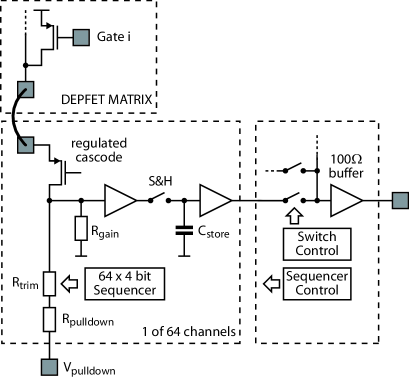
The block diagram of the first drain readout chip for DEPFET arrays with incomplete clear is sketched in Fig. 6. The drain current, which is fixed by the voltage of the gate rows, is converted into a voltage and sent to an ADC. The subtraction of the currents just after the clearing of the internal gate and at the end of the frame is done off-line using the ADC values. As motivated above, the voltages at the drains are kept nearly constant by means of a regulated cascode circuit. A constant current is subtracted from the drain current by a polysilicon resistor connected to the negative pull-down voltage. This voltage can be set well below the chip ground because no other components are connected to this node and no input protection is used. A large value for the pull-down voltage () and for the resistor was chosen to reduce its thermal noise below the thermal noise in the DEPFET device. The remaining current is converted into a voltage simply by means of a large value resistor. The value of this resistor is a compromise between high gain (reducing noise contributions of following stages) and dynamic range. Measurements of fabricated DEPJFET arrays showed that the drain currents for a fixed gate voltage varied by more than . This is due to inhomogeneities in the doping profiles and due to IR-voltage drops on source and drain signals. An individual adjustment of the subtracted current was therefore implemented to be able to keep the gain resistor high. The digital correction values are stored in a on-chip memory. They are used to increase or decrease the value of the pull-down resistor in 16 steps. Using this readout chip, a DEPFET array can be operated fully read out within the dynamic range at a gain of . The chip has been successfully used in the ’Bioscope’ system to operate a matrix of DEPJFETs [6] with an intrinsic speed of up to 1000 frames per second.
3.3 Source follower readout for DEPFETs with complete clear
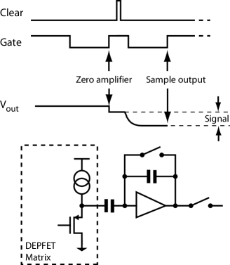
The source readout of a matrix with complete clear can be achieved by a voltage amplifier with a reset switch. As indicated in Fig. 7, the voltage amplifier (in this case implemented with a capacitive feedback) is set to a known state while the activated DEPFET row outputs the ’signal’ voltage. The change in the DEPFET output voltage after clearing the row (according to Eq. 1) is then amplified by the gain of the voltage amplifier. Note that large spikes on the source bus during the application of the clear pulse could drive the amplifier into saturation and degrade the output signal.
3.4 Fast drain readout for DEPFETs with complete clear
The block diagram of a chip for a fast drain readout assuming complete clear is sketched in Fig. 8. A regulated cascode circuit in every channel is used to keep the DEPFET drains at constant potential in order to decrease the influence of the drain bus capacitance. After selecting a DEPFET row for readout, the signal current is stored in a fast current memory cell (see below). The row is then cleared and the pedestal currents are subtracted from the stored signal current simply by summing currents (the current memory cell outputs the negative of its input current). A simple, fast current comparator is used to find the interesting hits, i.e. channels with a sufficiently large signal. A neighbor logic (not shown) could also select channels in the vicinity of hits for readout. When there is at least one hit in the row, the analog signal current and the binary hit flag of every channel are stored in a FIFO - like structure which consists of current memory cells and digital storage bits. Only the currents which are stored in hit cells are needed later so that all others cells can be turned off to save static power. The FIFO is thus filled permanently with events containing at least one hit. It serves as a buffer to cope with statistical fluctuations in the number of hits.
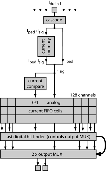
The second part of the chip empties the FIFO row by row. A fast binary hit scanner [7] can find up to two hits per clock cycle. The selected current values are digitized on-chip or sent off-chip together with their addresses. The scanner can process the FIFO row until no more hits are found so that there is no limitation on the number of hits per row as long as the average hit rate can be coped with.
Several other required circuit elements (row counting, time stamping of events) are not shown in Fig. 8. The proposed concept can be easily further improved if required. It is for instance possible to memorize the signal currents during several clock cycles in a bank of memory cells at the input and perform the subtraction of the pedestal current several clock cycles later. This could be advantageous if the clearing of the internal gate is not fast enough.
One of the crucial building blocks in this concept is the current memory cell [8] used for pedestal subtraction and for temporary analog storage in the FIFO-like structure. The basic concept of such cells is shown in Fig. 9. When switches and are closed, the gate voltage of the NMOS transistor settles to such a value that the sum of the input current and the bias current flow through the device. When is opened, this voltage is stored on the (parasitic) gate-source capacitance . The current through the device remains unchanged ideally. can now be opened without affecting the stored gate voltage. The current can be retrieved by closing . In the ideal case one gets . This is however not perfectly true due to charge injection onto when opening and due to the finite output conductance of the storage device and the current source. The devices have therefore been cascoded and two stages have been used to cancel charge injection. Preliminary measurements from a test chip designed in a technology using radiation tolerant layout techniques [9] have shown that shifting of currents is possible in less than with a precision of well below .
4 Summary
The intrinsic advantages of DEPFET devices like low noise, thin entrance window and non-destructive readout can be exploited on large areas by constructing DEPFET arrays. Gate and clear contacts are connected in rows while the drains or sources are connected in columns. Several chips to steer the array and to read out the voltages or currents at the bottom have been presented in this paper. The readout sequence is considerably simplified if the charge in the internal gate can be completely removed with a suited clear mechanism so that every pixel can be reset to a well defined state. The study of the clearing properties of new devices is therefore crucial.
5 Acknowledgements
The presented work has been carried out in collaboration with the Semiconductor Laboratory in Munich. The authors would like to thank the DEPFET team for their support.
References
- [1] Tesla Technical Design Report, DESY, Hamburg, ISBN 3-935702-00-0, 2001
- [2] J. Ulrici et al., Spectroscopic and imaging performance of DEPFET pixel sensors, Nucl. Inst. Meth. A465 (2001) 247
- [3] J. Kemmer and G. Lutz, New detector concepts, Nucl. Inst. Meth. A253 (1987) 365
- [4] P. Holl et al., these proceedings
- [5] P. Klein et al., Study of a DEPJFET pixel matrix with continuous clear mechanism, Nucl. Inst. Meth. A392 (1997) 254
- [6] P. Klein et al., A DEPFET Pixel Bioscope for the Use in Autoradiography, Nucl. Inst. Meth. A454 (2000) 152
- [7] P. Fischer et al., Mephisto - a 128 channel strip readout chips with real-time data sparsification and multi-hit-capability, Nucl. Inst. Meth. A431 (1999) 134
- [8] J. B. Hughes, et al., Switched Currents - A New TEchnique for Analog Sampled Data Signal PRocessing, Proc. of Int. Symp. Circuits and Systems (ISCAS), Portland, Oregon, May 1989, pp. 1584–1587
- [9] W. Snoeys et al., Layout techniques to enhance the radiation tolerance of standard CMOS technologies demonstrated on a pixel detector readout chip, Nucl. Inst. Meth. A439 (2000) 349