Development of a Hybrid Photo-Diode and its Front-End Electronics for the BTEV Experiment
Abstract
This paper describes the development of a 163-channel Hybrid Photo-Diode (HPD) to be used in the RICH Detector for the BTEV Experiment. This is a joint development project with DEP, Netherlands. It also reports on the development of associated front-end readout electronics based on the va_btev ASIC, undertaken with IDEAS, Norway. Results from bench tests of the first prototypes are presented.
1 INTRODUCTION & MOTIVATION
The most problematic decision in the design of any RICH Detector is the choice of the photon detector technology. The context of the present photon detector R&D effort is the design of the RICH Detector for the BTEV Experiment [1], in which there is need to efficiently image visible Cherenkov photons from a C4F10 gas radiator over a large area.
For BTEV, we require that the RICH photon detector have high single-photon detection efficiency, high responsivity in the visible spectrum (280–600 nm), large area coverage (for a 6.2 m2 detector plane), small dead area (for large overall efficiency), modestly high resolution (), fast time response (for the Tevatron bunch crossing of 132 nsec or 7.6 MHz), withstand our radiation environment and fringe magnetic field, and have long life and high reliability (over an experiment life of 10 years).
After consideration of extant technologies for high-efficiency, large-area photon detection (MA-PMTs, FP-PMTs, etc.), we decided that Hybrid Photon Detectors (HPDs, also Hybrid Photo-Diodes) had the potential to meet our requirements, and we have pursued a solution based on this technology. Hence, a HPD development project was begun, jointly between Syracuse University and DEP (Netherlands) to produce the detector; and in parallel, a readout electronics development project was begun, jointly with IDEAS (Norway), to produce the front-end electronics.
2 HYBRID PHOTON DETECTORS
2.1 Basic Design and Operation
The basic design of the HPD is a vacuum tube device—a “hybrid” device, i.e., the marriage of a single-stage Gen-I image intensifier and a Silicon diode.
In this design, a S20 multialkali photocathode is deposited on a spherical Quartz window. Incident photons convert at the photocathode and enter an acceleration stage, with cross-focused electron optics, requiring applied voltages up to 20 KV. The electrostatics transports photoelectrons onto a Silicon diode sensor, consisting of channels of parallel Si PIN diodes (pixels). The reverse bias is positive, so holes are collected in a few nsec. There is a 4:1 reduction in diameter from window to diode.
2.2 Expected Performance
The expected performance of the HPD is promising: it is designed to have sensitivity to single photoelectrons, a large active area (80%), fast response time, highly linear response (with ), good uniformity (10% variation), and low crosstalk (2% between pixels).
The HPD comes with its own set of “issues”, as does any photon detector. It requires a very high applied voltage (VHV, 20 KV level) to each of three electrodes, which will be challenging to distribute over a large area array. However it has only a very low current draw on the power supply (few nA). It has a small signal, typically 5000 e-, demanding very low noise electronics for good SNR. As an electron-drift device, it is sensitive to fringe magnetic fields, needing significant external shielding. It is subject to radiation damage, as the Si-diode is not rad-hard (however for BTEV, this is not a problem). It ages as the photocathode degrades due to ion feedback (again not a problem for BTEV, with low integrated intensities). Finally, there is the potential for a “ghost” image caused by incident photons reflecting from internal surfaces, and converting at the photocathode from the interior of the HPD. The intensity of this image needs to be determined.
2.3 HPD Development for BTEV
The starting point for HPD development for the BTEV RICH is the 61-channel commercial tube PP0380V (developed by LHCb and DEP [3]). The goal is to increase pixel resolution to meet our spatial requirements without “breaking the vacuum”, i.e., to increase the number of pixels on the Si-diode, while retaining the same electrostatics and the capability of using external readout electronics.
The result of this development is the new 163-channel HPD: PP0380AT. A new diode was designed and manufactured, with 163 hexagonal pixels (‘hexels’) having 1.4 mm pitch flat-to-flat in a close-packed arrangement, surrounded by a guard ring. This was mated with the existing vacuum body. Pins on the new diode carrier take signals out, so external electronics can be used. This modular design was consciously chosen to provide easier testing, easier replacement, and easier development of the entire system.
Two new 163-channel HPDs have been delivered, and are under test at Syracuse. The quantum efficiency at 320 nm is 22% and 25%, respectively. The leakage current is under 20 nA total for all pixels. These first tests were made with the analog readout chip va_rich, used in the CLEO-III RICH [6]. The development of our new fast digital readout chip va_btev is discussed below.
3 HPD First Results
3.1 Low Light Level Detection
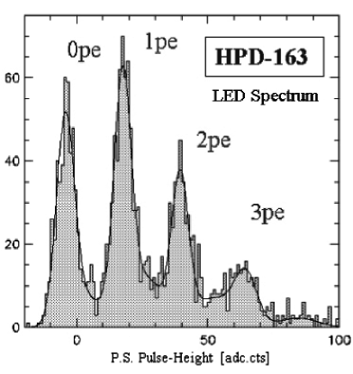
Using a test-bench setup consisting of a pulsed LED, 20 KV high voltage system, analog va_rich readout, and CAMAC-based data acquisition, we have obtained the pulse-height spectrum shown in Fig. 1. The spectrum shown is both pedestal and common-mode subtracted. One can clearly see peaks corresponding to 0pe, 1pe, 2pe, etc. Other channels are similar; all channels are responsive. The fit is made to multiple Gaussians, including the backscattered electron background for which it yields an average of 0.182. This should be compared to an expected value of 0.173 at 20 KeV [7]. The width of the peaks is dominated by electronic noise and time jitter in the LED. Nevertheless single photoelectrons are clearly detected.
3.2 Gain and Linearity
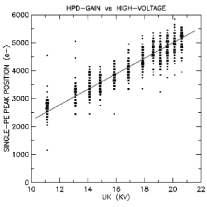
The position of the single-photoelectron peak above pedestal in electrons is the gain (in units of e-/pe). Fig. 2 shows a scan of gain vs applied cathode voltage , for all channels. The theoretical gain curve,
| (1) |
is overlaid. Here is the barrier potential, and . We obtain a gain of 5000 at 20 KV, as expected. Additionally, we see linearity of gain across the VHV scan, as expected. The gain uniformity at 20 KV is 10% RMS, for all pixels.
3.3 Signal-to-Noise
A well-separated single-photoelectron peak is necessary for good single-photon detection, particularly in the case of binary readout. One may define the significance of separation of the single-photoelectron peak from pedestal as a measure of signal-to-noise, viz.,
| (2) |
with the mean and RMS of the Gaussian fits denoted conventionally. A scan across applied high voltage yields a signal-to-noise for . This value is just below our design expectation of 7, even though it is obtained using the slower analog electronics of our test setup.
3.4 Magnetic Field Effects
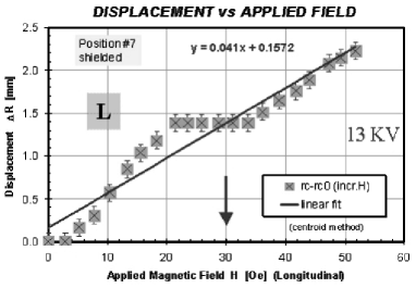
Preliminary measurements of magnetic field effects on HPD performance were made by placing the HPD in a pair of Helmholtz coils, having better than 5% field uniformity in the central region. The point spread function (PSF) was generated by a LED through a pinhole in a baffle at the face of the HPD. The pinhole was moved to various locations and the position of the PSF spot was reconstructed by a centroid method. One expects that the photoelectron trajectories are distorted by the applied field, so the centroid movement across the pixel array can be traced as a function of applied field and shielding.
For the unshielded case, the centroid moves as expected when either transverse or longitudinal applied fields are varied. There is a step in the radial displacement of the centroid from its initial position as it crosses a pixel boundary under the influence of increasing field. Hence, the applied field required to displace the PSF a single pixel is determined from this as 9 G, for transverse field at half radius. This number is larger than one would naively expect, due to the Kovar body of the HPD providing some shielding capacity at low fields. This is consistent with our simulations of the HPD, and is confirmed by making a hysteresis loop in the displacement.
For the shielded case, the HPD is surrounded by a tube of CO-NETIC AA foil, arranged in four layers of 0.25 mm each, with the HPD recessed 5 cm inside the tube. Again, both transverse and longitudinal applied fields are varied. A typical result for the displacement is shown in Fig. 3, in which the step between pixels may be clearly seen. The location of the image represents an average response to the longitudinal field. The high voltage in this measurement was limited to 13 KV, see below. Hence, on the average, the applied field required to displace the PSF a single pixel is 60 G (T) and 30 G (L).
For BTEV, we expect to reduce the dipole fringe field to 30 G maximum modulus in the region of the HPDs. We would like to stay below the intrinsic resolution of the device (0.4 mm) up to this limit, in order not to have to depend too much on software corrections. The present limits are 18 G (T) and 8 G (L), on average. Additional studies are being carried out.
4 HPD Operational Experience
Our overall operational experience with the HPD, given the “issues” mentioned above, is promising. There are small turn-on effects, but the device stabilizes as the electronics thermalizes. The humidity must be low in the detector volume for stable operation. The biggest concerns are related to the VHV distribution.
There is a strong effect on the readout noise level (both total and common-mode subtracted) introduced by ripple in the high voltage power distribution. We investigated this by making a scan of the power supply rejection ratio in frequency and amplitude. The profile matches that of the va_rich itself, indicating a strong coupling to the readout inputs. The noise response of the system degrades significantly above 10 mV pp ripple, and at frequencies above 2 kHz. However, the noise is reduced to an acceptable level by simple RC filtering local to the HPD, using appropriate VHV components.
In operation with a magnetic shield in close proximity there will be corona discharges unless the bare HPD electrode and the shield are properly insulated. This is challenging in a close-packed array, where radial space is at a premium. We have made a series of tests of insulating schemes to determine which is best for stable operation. We have modified the HPD design with an insulation scheme being fabricated which we believe will make the problem manageable.
5 Front-End Electronics Development
The development of the readout electronics for the BTEV RICH HPD was undertaken with the goal of producing an ASIC and a hybrid board for low-noise, fast readout with minimum pile-up at Tevatron rates. The starting point for development was the Viking front-end VA_32/75 (amplifier) and TA32C (discriminator).
5.1 The va_btev Chip
The va_btev ASIC itself has 64 channels of parallel analog input with 64 parallel digital current outputs. It has low noise, with an ENC specification of 500 e- at , and a readout design goal of SNR = 7:1. The peaking time of 75 nsec matches the Tevatron rate of 132 nsec. The fall time (200 nsec) extends the signal beyond the next crossing for a given hit channel, however there is little loss of efficiency due to low occupancy. The ASIC has a global threshold setting for the chip, as well as fine tuning of individual channel thresholds with a 4-bit DAC. It has a calibration input connected to an input multiplexer.
The design for an single channel is as follows. The input pad is DC-coupled to a charge-sensitive preamplifier, followed by an optional gain stage, and a shaper. This analog section is ac-coupled to a comparator that implements the global and fine thresholds. The output is fed to a monostable multivibrator which produces a current level output for each channel. It also feeds into a Fast-OR output.
5.2 The VA_BTEV Hybrid Board
The VA_BTEV hybrid PCB is comprised of three va_btev ASICs, followed by parallel level-adapters, an FPGA for programmable interfacing, and local power regulation. The readout is binary. One hybrid will service a single HPD.
The first development iteration has been completed, with two prototypes tested. These boards are fully rigid, while the next iteration will feature a flex-circuit neck between the ASICs and the other components in order to negotiate mechanical constraints. Additionally, this design isolates the analog and digital sections of the board for best noise performance. The second generation also includes redesigned power regulation and other improvements. Prototypes have been fabricated and are undergoing testing.
6 Front-End Electronics Testing
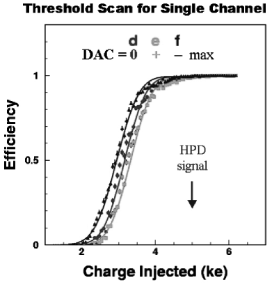
Tests of the VA_BTEV hybrid prototype have been performed, using a test-bench setup designed for full characterization and data acquisition. A threshold scan was performed by injecting a variable impulse charge through a 1.0 pF capacitor, giving a resultant curve as shown in Fig. 4. The global threshold is set at a nominal value of 3100 e- for the entire chip, and the 4-bit fine threshold is adjusted to zero and its extremes, giving the three curves shown. All curves reach full efficiency for charge collection at the HPD signal level of 5000 e-. These curves were fit, yielding 350 e- noise (erf sigma) for this channel. For all channels in this first development iteration, the noise ranges from 275–1000 e-, yielding SNR 18–5, respectively.
The noise as measured is lower for positive injected charge. This is fortunate for the HPD in which holes are collected, so this effect works in our favor. Inclusion of the gain stage lowers the noise but tends to produce a loss of efficiency at higher level signals. To fully understand this, we are making more timing studies.
Integration tests of the hybrid prototypes with the HPD are in progress.
7 Summary and Future
We are engaged in a development program to produce a 163-channel HPD and its associated electronics for the BTEV experiment. We have confirmed the basic properties of this HPD, which works as expected. We need to continue with operational and system tests. We have developed the fast front-end va_btev ASIC and hybrid board. The first prototypes have been tested successfully, and establish a proof-of-principle of the design. Noise, timing, and integration studies are underway. A beam test of 15 fully-instrumented HPDs is scheduled for Spring 2003 at FNAL.
References
- [1] S. Blusk, “Design and Expected Performance of the BTeV RICH”, these proceedings.
- [2] A. Braem et al., Nucl. Instr. and Meth. A 433 (1999) 153.
- [3] S. Easo, “Development of the RICH Detectors in LHCb”, these proceedings; and M. Alemi et al., Nucl. Instr. and Meth. A 449 (2000) 48. This is the development effort from which we have derived the most direct benefit.
- [4] P. Cushman et al., Nucl. Instr. and Meth. A 442 (2000) 289.
- [5] R. DeSalvo et al., Nucl. Instr. and Meth. A 315 (1992) 375.
- [6] S. Stone, “Construction and Operational Experience with the LiF-TEA CLEO-III RICH Detector”, these proceedings.
- [7] E. H. Darlington, J. Appl. Phys. 8 (1975) 85.