Pixel Detectors for Particle Physics and Imaging Applications
Abstract
Semiconductor pixel detectors offer features for the detection of radiation which are interesting for particle physics detectors as well as for imaging e.g. in biomedical applications (radiography, autoradiography, protein crystallography) or in Xray astronomy. At the present time hybrid pixel detectors are technologically mastered to a large extent and large scale particle detectors are being built. Although the physical requirements are often quite different, imaging applications are emerging and interesting prototype results are available. Monolithic detectors, however, offer interesting features for both fields in future applications. The state of development of hybrid and monolithic pixel detectors, excluding CCDs, and their different suitability for particle detection and imaging, is reviewed.
keywords:
pixeldetector , semiconductor detectorTalk given at the 9th European Symposium on Semiconductor Detectors, Elmau, Germany, June 2002
Introduction
The requirements on semiconductor pixel detectors for charge particle detectors in high energy physics compared to those from imaging can be very different. In particle physics experiments individual charged particles, usually triggered by other subdetectors, have to be identified with high demands on spatial resolution and timing. In imaging applications the image is obtained by the un-triggered accumulation (integrating or counting) of the quanta of the impinging radiation, often also with high demands (e.g. 1 MHz per pixel in certain radiography or CT applications). Si pixel detectors for high energy charge particle detection can assume typical signal charges collected at an electrode in the order of 5000-10000 electrons even taking into account charge sharing between cells and detector deterioration after irradiation to doses as high as Mrad. In tritium autoradiography, on the contrary, or in low energy Xray astronomy the amount of charge to be collected with high efficiency can be much below e. The spatial resolution is governed by the attainable pixel granularity to a few to about 10m at best, obtained with pixel cell dimensions in the order of m to m. The requirements from radiology (mammography) are similar, while some applications in autoradiography require sub-m resolutions, not attainable with present day pixel detectors. For applications with lower demands on the spatial resolution (m)) but with demands on real time and time resolved data acquisition, semiconductor pixel detectors are however attractive.
Thin detector assemblies are mandatory for the vertex detectors at collider experiments, in particular for the planned linear collider. While silicon is almost a perfect material for particle physics detectors, allowing the shaping of electric fields by tailored impurity doping, the need of high photon absorption efficiency in radiological applications requires the study and use of semiconductor materials with high atomic charge, such as GaAs or CdTe. For such materials the charge collection properties are much less understood and mechanical issues in particular those related to hybrid pixels are abound, most notably regarding the hybridization of detectors when they are not available in wafer scale sizes. Last but not least the cost-performance ratio is an important factor to consider if an imaging application should be commercially interesting.
Hybrid Pixel Detectors for Particle Physics
In the ”hybrid pixel technique” sensor and FE-chips are separate parts of the detector module connected by the small conducting bumps applied by using the bumping and flip-chip technology. All of the LHC-collider-detectors [1, 2, 3] ALICE, ATLAS, and CMS, LHCb for the RICH system [4], as well as some fixed target experiments (NA60 [5] at CERN and BTeV [6] at Fermilab) employ the hybrid pixel technique to build large scale () pixel detectors. Pixel area sizes are either rectangular (typically m m as for ATLAS) or quadratic (m m as for CMS). The detectors are arranged in cylindrical barrels of layers and disks covering the forward and backward regions. The main purpose that these detectors must serve is (a) identification of short lived particles (e.g. b-tagging for Higgs and SUSY signals), (b) pattern recognition and event reconstruction and (c) momentum measurement, in this order of importance. Among the technical issues of high demand which must be addressed the need to withstand a total (10 years) particle fluence of neq corresponding to a radiation dose of about Mrad is the most demanding one. The discovery that oxygenated silicon is radiation hard with respect to the non-ionizing energy loss of protons and pions [7] saves pixel detectors at the LHC for which this radiation is most severe due to their proximity to the interaction point. electrode in n-bulk material sensors have been chosen to cope with the fact that type inversion occurs after about neq. After type inversion the -diode sits on the electrode side thus allowing the sensor to be operated partially depleted. Figure 1(a) shows the layout of the ATLAS pixel sensor [8]. The n+ pixels are isolated against each other by the moderated p-spray technique [8, 9]. The bias grid at the bottom allowes to test the sensor before bonding to the electronics ICs is made. All pixels are set under voltage by the punch through biasing mechanism.
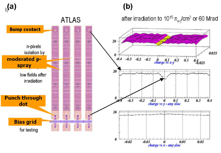
Figure 1(b) show the charge collected in two adjacent pixels after irradiation with protons/cm2, the full LHC dose after 10 years. A tolerable loss in charge collection efficiency is observed at the punch-through dot, which goes at the expense of the biasing feature which is too important to be sacrificed, and at the edge of the pixel. Everywhere else the collection even after this high dose is homogeneous. The sensors can be operated after irradiation with bias voltages in excess of V in full depletion. Pixel sensors for the LHC detectors are close to or already in production in large quantities.
The requirements on the FE-chip also impose severe constraints on noise, threshold dispersion, timewalk and power consumption. After several chip generations first in radiation soft CMOS and BiCMOS technologies and later in the radiation hard DMILL and 1/4 micron technologies have at last produced FE-ICs with the required performance and decent yield in excess of . After irradiation to the full LHC dose, the ATLAS 1/4 micron pixel chip FE-I shows noise values of about e and threshold dispersions in the range of e after threshold tuning. The power consumption per pixel is about W.
The process of chip and sensor connection called hybridization is done by fine pitch bumping and subsequent flip-chip which is achieved with either PbSn (solder) or indium bumps at a failure rate of . Figure 2 shows rows of m pitch bumps obtained by these techniques.
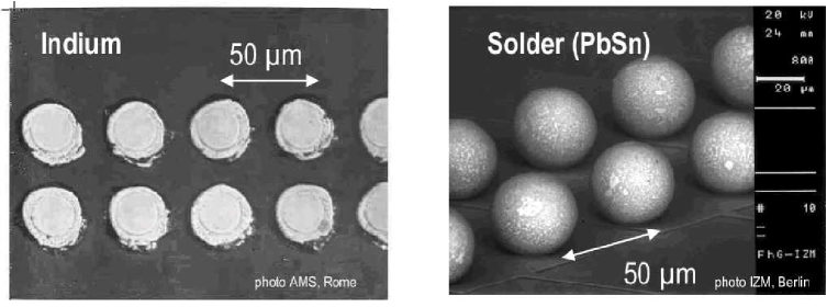
Indium bumps are applied using a wet lift-off technique applied on both sides (sensor and IC) [10]. The connection is obtained by thermo-compression. The Indium joint is comparatively soft and the gap between IC and sensor is about m. PbSn bumps are applied by electroplating [11]. Here the bump is galvanically grown on the chip wafer only. The bump is connected by flip-chipping to an under-bump metallization to the sensor substrate pixel. Both technologies have been successfully used with 8” IC-wafers and 4” sensor wafers.
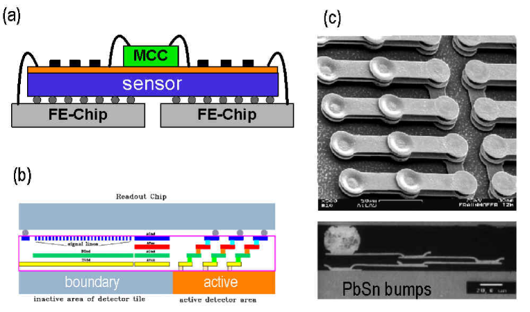
In the case of ATLAS sixteen FE-chips are bump-connected to a silicon sensor to form a of 2.1 cm by 6.4 cm area (fig. 3(a)). The I/O lines of the chips are connected via wire bonds to a kapton flex circuit glued atop the sensor. The flex houses a module control chip (MCC) responsible for front end time/trigger control and event building. The total thickness at normal incidence is in excess of of a radiation length.
The modules are arranged in ladders (staves) and cooled by evaporation of a fluorinert liquid ( or ) at an input temperature below in order to maintain the entire detector below to minimize the damage induced by radiation. This operation requires pumping and the cooling tubes must stand bar pressure if pipe blocking occurs. All detector components must withstand temperature cycles between and room temperature.
In summary, the Hybrid Pixel Technology is the present day technology for large area pixel detectors in particle physics. Several pixel vertex detectors are in production for LHC- and other experiments. Some potentially major issues still exist, most notably yield issues which in this technology come into play in many areas as chip-wafer and sensor-wafer yields, bumping and flip-chipping yields, as well as burn-in yields of modules with 16 ICs and about 50000 individual amplifier channels.
What are the possible future advances and directions and what are the limitations of the hybrid pixel technology? The area of a pixel cell is limited by the readout circuitry obtainable for a given area. With the availability of chip technologies with small structure sizes (m) the target pixel size can be made substantially smaller than planned for the first generation of large area hybrid pixel detectors. Area sizes of m2 or somewhat below are, however, at the limit for this technology in my opinion. The limit for small pitch bumping is in the order of m [12]. An interesting alternative to the flex-kapton solution to provide power and signal distribution to and from the module is the so-called Multi-Chip-Module Technology deposited on Si-substrate (MCM-D), pioneered by IZM (Berlin), for pixel particle detectors in collaboration with Wuppertal University [13]. A multi-conductor-layer structure is built up on the silicon sensor. This allows to bury all bus structures in four layers in the inactive area of the module thus avoiding the kapton flex layer and any wire bonding at the expense of a small thickness increase of . Figure 3(b) illustrates the principle and fig. 3(c) shows scanning electron microphotographs (ref. IZM, Berlin) of a via structure made in MCM-D technology.
Hybrid Pixel Detectors for Imaging Applications
Radiology
There is a vast amount of radiology detection and imaging techniques. The discussion in this paper will be limited to an application which possibly opens new directions in radiology due to fully digital imaging, i.e. pixel detectors with individual X-ray photon counting in every pixel cell. This approach offers many features which are very attractive for X-ray imaging: excellent linearity and an infinite dynamic range (at least in principle), optimal exposure times and a good image contrast compared to conventional film-foil based radiography thus avoiding over- and underexposed images. There are very interesting developments using integrating methods such as flat panel imagers based on a-Sci [14] or a-Se technologies [15], which are to be considered the state of the art in large area radiography. Their review, however, is beyond the scope of this paper and is referred to dedicated conferences [16].
Two counting hybrid pixel detector developments are called MEDIPIX [17], a CERN-based collaboration and MPEC [18] at Bonn University. The challenges to be addressed in order to become competitive with integrating systems are: high speed ( MHz) counting with at least 15 bit, operation with very little dead time, low noise and particularly low threshold operation with small threshold dispersion values. In particular the last item is important in order to allow homogeneous imaging of soft Xrays. It is also mandatory for a differential energy measurement, realized so far as a double threshold with energy windowing logic [19, 20]. A differential measurement of the energy, exploiting the different shapes of Xray spectra behind for example tissue or bone, can enhance the contrast performance of an image. The idea of using a linear feedback shift register as a small counter which fits in a pixel area was first realized in [21] and is implemented in both, MPEC and MEDIPIX, circuits. Finally, for radiography high photon absorption efficiency is mandatory, which renders the not easy task of high Z sensors and their hybridization necessary.
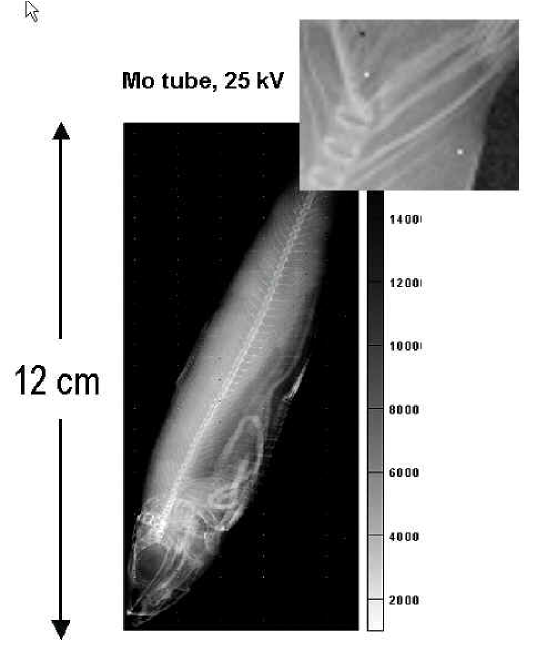
The MEDIPIX chip (version 2) [20] uses , m m large pixels fabricated in m technology, energy windowing via two tunable discriminator thresholds, and a 15 bit counter. The maximum count rate per pixel is about 1 MHz. Figure 4 shows an X-ray scan of a sardine taken in successive scanning steps with the MEDIPIX1 chip ( pixels, m m) using a Si sensor. GaAs sensors have also been successfully operated.
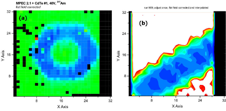
Imaging sensor systems [22, 23] using the MPEC chip have been made also with high Z semiconductors for more efficient X-ray absorption. A technical issue here is the bumping of individual die sensors of Cd(Zn)Te or GaAs. This has been solved at ISAS, Tokyo in collaboration with Mitsubishi Industries and Bonn University by employing double Au-stud bumps with In-filling material on order to account for thickness inhomogeneities in the sensor surface [23]. Figure 5 shows an image of a nut and that of a screw obtained with a CdTe sensor using the MPEC2.3 counting chip. The MPEC chip features pixels (m m), double threshold operation, 18-bit counting at MHz per pixel as well as low noise values (e with CdTe sensor) and threshold dispersion (e after tuning).
Both MPEC and MEDIPIX developments now address modules with a larger detection area () and high-Z sensors. While the counting pixel approach is new and interesting for imaging applications, it will be difficult to compete on a short time scale with already commercially available integrating systems such as flat panel imagers [14, 15]. The possible market value of photon counting pixel systems is not yet explored.
Crystallography
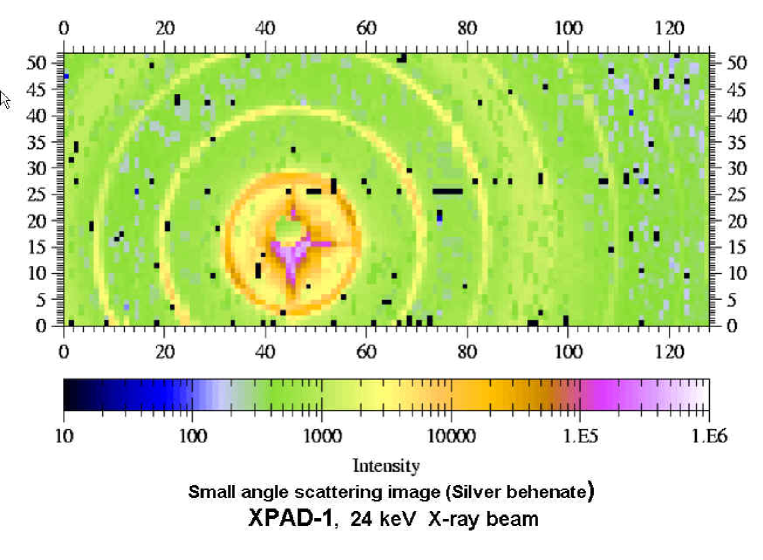
Counting hybrid pixel detectors are also starting to become used in protein crystallography with synchrotron radiation. Here the challenge is to image Bragg patterns produced by scattered Xray photons of typically 6 keV or higher at a high rate (typ. MHz/pixel). The typical spot size of a diffraction maximum is m, calling for pixel sizes in the order of m. The high linearity of the hit counting method and the absence of so-called ”blooming effects”, i.e. the response of non-hit pixels in the close neighbourhood of a Bragg maximum, makes these detectors very appealing for protein crystallography experiments. Developments are underway for ESRF (Grenoble, France) and SLS (Swiss Light Source at the Paul-Scherrer Institute, Switzerland) beam lines. The XPAD detector [24] (m m pixels) planned for ESRF beam lines has modules with 10 chips bonded to a cm2 silicon substrate. The PILATUS detector [25] at the SLS (m m pixels) is made of sixty 16 chip modules each covering cm2, i.e. a total area of cm2. The maximum count rate of both detectors is MHz/pixel. A delicate threshold tuning question remains to obtain a homogenous response function of the detectors also at the pixel boundaries where a loss of charge on a pixel occurs due to charge sharing and may lead to hit losses. Figure 6 shows a diffraction image of Ag-Behenate obtained with the XPAD detector [26].
In conclusion, the hybrid pixel technique has been established also for imaging using silicon and high-Z material such as GaAs or CdTe. The method of photon counting in every pixel offers at least in principle the possibility of an infinite dynamic range and linearity, giving hope for a new quality of experiments with synchrotron light detectors. For radiology the use of double (multiple) thresholds is interesting to enhance the contrast performance. It will, however, be very demanding to go much beyond a count rate of about 1 MHz per pixel and to produce large area detectors.
Monolithic Pixel Detectors
Monolithic pixel detectors, in which amplifying and logic circuitry as well as the radiation detecting sensor are made from on piece of silicon, has been the dream of semiconductor detector physicists. The first monolithic pixel detector, successfully operated in a particle beam was made by Snoeys and collaborators [27] as early as in 1992. They used a p-type bulk with n-diffusion layer with ohmic contacts as pixellated collection electrodes on the top allowing only PMOS transistors in the active detector area. No large scale detector evolved from this approach.
A new era calling for monolithic pixel or CCD vertex detectors is that of future colliders most notably linear colliders, where very low () material per layer, small pixel sizes (mm) and very high rate capability (80 hits/mm2/ms) is required. This is due to the very intense beam strahlung of a narrowly focussed electron beams close to the interaction region which produces electron positron pairs in vast numbers. High readout speeds of MHz with s frame time are required. These challenges are addressed at the TESLA collider [28] by CMOS CCDs [29], CMOS Active Pixel Sensors [30] and DEPFET pixel detectors [31, 38].
CMOS Active Pixels
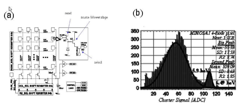
CMOS active pixel detectors as they are used in CMOS cameras are suited also for the detection of minimum ionizing particles. However their fill factor is less than and the total chip area is small. Mimosa111minimum ionizing MOS array Active Pixel Sensors (MAPS) [30] have been developed to overcome these deficiencies. As shown in fig. 7 the epitaxial layer of a standard CMOS (m or m) process is used for the generation of electron-hole pairs. They are trapped between potential barriers on both sides of the epi-layer and reach, by thermal diffusion, an n-well/p-epi collection diode, rendering small pixel sizes a necessity and not a demand. The sensor is depleted only directly under this n-well diode. Only here full charge collection is obtained. Matrix operation is done using a standard 3-transistor readout commonly employed by CMOS matrix devices (see fig. 8(a)). A line of the matrix is selected by transistor M3, the signal is readout via a source follower stage (M2), and reset by transistor M1. The charge obtained for a signal from a high energy particle is in the order of only e or less, the collection time is 100ns, but low noise values (15–30e) and small pixel sizes (m m) can be achieved. This is demonstrated in fig. 8(b) which shows the response to a 55Fe keV Xray signal. The small peak corresponds to hits entering in the small depleted region under the n-well. The large peak is due to Xrays absorbed in the undepleted area of a pixel.
Summarizing PRO’s and CON’s of CMOS monolithic pixel detectors for particle physics I would conclude that from the above mentioned ‘dream’ of fully monolithic CMOS charge sensing, amplification, readout and logic, one is still a bit away. While the low cost (potentially $ for pixels) for ‘off-the-shelf’ CMOS sensors is indeed a very attractive feature, a area fill factor still requires a special development and RD programme (like MIMOSA APS). In the active area, due to the n-well collection diode, no CMOS (only NMOS) circuitry is possible. The voltage signals are very small (mV), of the same order as transistor threshold dispersions which at least requires some dedicated design effort. At present [32] also a severe radiation tolerance issue exists. While the MAPS sensors withstand non-ionizing radiation (neutrons) up to about n/cm2, ionizing radiation, even soft X-rays, impose a serious problem for present designs as the devices stop functioning already after krad. This is under investigation. It seems that the radiation sensitivity is not inherently due to the MAPS sensor structure itself. Last, but not least, the necessity of a sufficiently thick epitaxial layer as charge collection layer, renders only a few processing technologies suited for sensors. With the rapid change of commercial process technologies this also is an issue of concern. The CMOS camera market may save these developments.
DEPFET Pixels
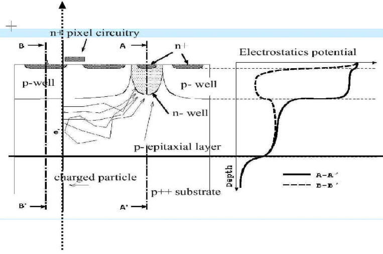
The DEPFET (Depletion Field Effect Transistor) pixel principle [33] has been and is being developed for three very different application areas: particle physics vertex detection [31], X-ray astronomy [34, 35] and for biomedical autoradiography [36]. Figure 9 shows the principle of operation of this device. On a sidewards depleted bulk (Si) the potential for electrons is formed such that the minimum is located about m below the top surface.
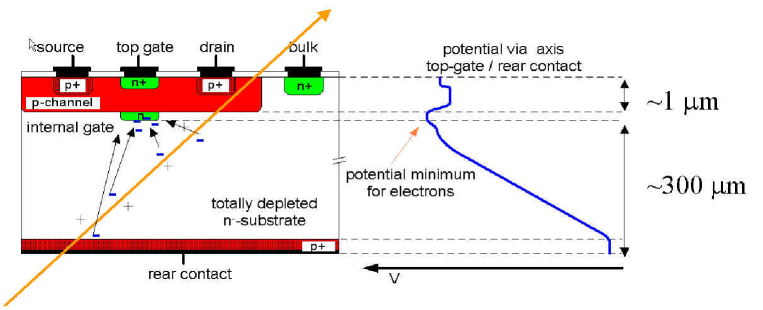
By additionally shaping the potentials of bulk, source and drain of an implanted JFET or MOS transistor on the pixel’s surface, aided by a deep-n implantation under the gate region, a local potential minimum for electrons is formed under the transistor channel which acts as an ‘internal gate‘. The holes created by the impinging radiation drift towards the rear contact, the electrons are collected and stored in the potential bucket of the internal gate, thereby changing its potential resulting in a modulation of the channel current of the implanted transistor. The collected electrons are removed from the internal gate by a clear pulse applied to a dedicated CLEAR contact outside the transistor reagion or by other clear mechanisms e.g. through the external gate by punch-through to the internal gate.
The very low input capacitance and the in situ amplification (i.e. charge to current conversion) of the device makes DEPFET pixel detectors very attractive for low noise operation. The latter is very important for low energy X-ray astronomy and for autoradiography applications. For particle physics, where the signal charge is large in comparison, this feature can be used to design very thin detectors [31, 37] (m) with very low power consumption when operated as a row-wise selected matrix. Depending on the application, i.e. for very low noise operation in spectroscopy or very fast readout in particle physics the device is operated in source follower readout mode or drain current readout mode (see paper given at this conference [38]). Figure 10 shows the response of a single DEPFET pixel operated in source follower readout mode to an 55Fe source. The measured energy resolution is
at a temperature of C. Very similar values were also obtained at room temperature. The noise contribution is dominated by Fano noise ( at 6 keV and RT). The DEPFET structure itself contributes with , mostly 1/f, channel noise.
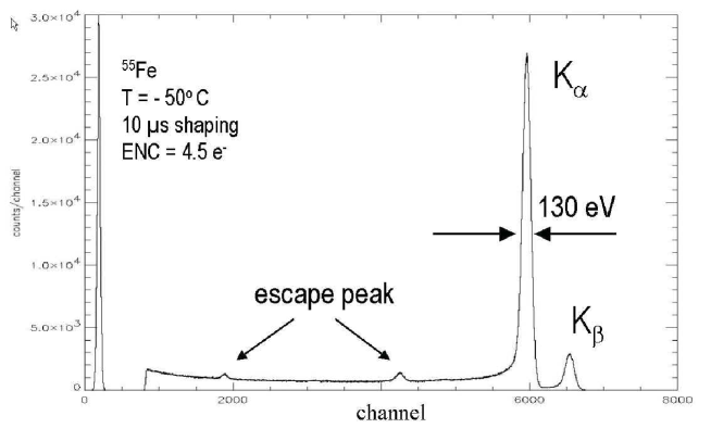
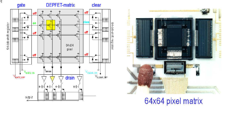
Figure 11 shows the principle of operation of a large pixel matrix [39]. Rows are selected by applying a voltage to the external gate of a row. Drains are connected column-wise. The drain current of each pixel in a selected row is detected and amplified in a dedicated amplification circuit. Pedestals are taken the same way several cycles before and subtracted. Finally, clear pulses are applied to the clear contacts to empty the internal gates.
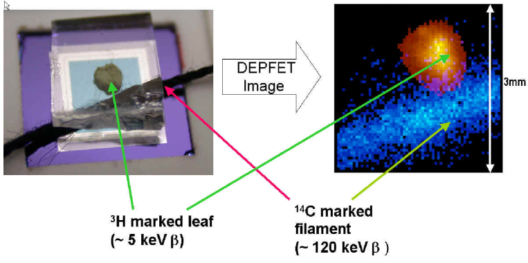
DEPFET pixel matrices are presently being developed for low noise high energy resolution operation in the X-ray satellite project XEUS [34] and for high speed, high spatial resolution in the TESLA vertex detector [31]. A DEPFET Bioscope matrix has already been used [39] in autoradiographical imaging of tritium marked biological samples. Figure 12 demonstrates the successful separation of two different radio markers (3H and ) with high spatial resolution [40].
Summary
Driven by the demands for high spatial resolution, high rate particle detection in high energy physics, semiconductor pixel detectors have also started to become exploited for imaging applications. Hybrid pixel detectors, in which sensor and electronic chip are separate entities, connected via bump bonding techniques represent today’s state of the art for both, particle detection and imaging applications. Monolithic detectors, in the form of CMOS sensors, are already used for imaging in CMOS cameras. For the detection of high energy particles they are so far of limited use mainly because their fill factor is smaller than 1, i.e. less than 100% detection coverage, and their radiation tolerance is weak. The next generation of collider experiments, however, will have to target monolithic pixel detectors. Present approaches in this direction are: Monolithic Active Pixel Sensors (MAPS) which try to overcome the limitations of CMOS camera chips, and pn-DEPFET Pixel Detectors which are also very attractive for (low energy) Xray astronomy and autoradiographical imaging.
Acknowledgements
I would like to thank Woitek Dulinski for an honest discussion of the features and technicalities of the MIMOSA Active Pixel concept.
References
- [1] Technical Design Report of the ATLAS Pixel Detector, CERN/LHCC/98-13 (1998).
-
[2]
CMS, the Tracker System Project, Technical Design Report,
CERN/LHCC/98-006 (1998);
W. Erdmann, The CMS pixel detector, Nucl. Inst. Meth. A447 (2000) 178-83. -
[3]
ALICE Technical Design Report, CERN/LHCC 99-12 (1999);
F. Antinori, A pixel detector system for ALICE, Nucl. Inst. Meth. A395 (1997) 404-409. - [4] T. Gys, The pixel hybrid photon detectors for the LHCb-RICH project Nucl. Inst. Meth. A465 (2001) 240-246.
-
[5]
A. Baldit et al., CERN-SPSC-2000-010 (2000);
C. Lourenco, E. Radermacher, CERN-SPSC-2002-025 (2002). - [6] BTeV Proposal (2000), FNAL document http://www-btev.fnal.gov/DocDB/0000/000066/002/index.html.
- [7] ROSE Collaboration, G. Lindström et al., Nucl. Inst. Meth. A466 (2001) 308-326; G. Lindström, paper presented at this conference (9th European Symposium on Semiconductor Detectors, Elmau 2002).
- [8] M. S. Alam et al., Nucl. Inst. Meth. A456 (2001) 217-232.
- [9] R. Richter, paper presented at this conference (9th European Symposium on Semiconductor Detectors, Elmau 2002).
- [10] C. Gemme, Study of Indium bumping for the ATLAS pixel detector, Nucl. Inst. Meth. A465 (2001) 200–203.
-
[11]
G. Engelmann, J. Wolf, L. Dietrich, S. Fehlberg, O. Ehrmann and
H. Reichl, Proc. 1999 Joint International Meeting of the
Electrochemical Society, Hawaii 1999, Vol. 99-2 p. 907;
J. Wolf, PbSn60 Solder Bumping by Electroplating, Pixel2000 Workshop, Genova, Italy, June 2000. - [12] O. Ehrmann, Fraunhofer Institut IZM, Berlin, private communication
- [13] P. Gerlach, C. Linder, K.H. Becks, Nucl. Inst. Meth. A473 (2001) 102-106 and references therein; M. Töpper, Intl. Conf. on High Density Packaging and MCMs, Denver, Colorado, April 1999.
-
[14]
T. Ducourant et al., Proc. SPIE 3977 (2000) 14-25;
N. Jung et al., Proc. SPIE 3336 (1998) 396-407. - [15] O. Tousignant et al., Proc. SPIE 4682 (2002) 503-510.
- [16] see for instance: Proc. of SPIE Conference on Medical Imaging 2002, San Diego
-
[17]
M.Campbell, E.H.M.Heijne, G.Meddeler, E.Pernigotti, W.Snoeys,
IEEE Trans. Nucl. Sci. 45(3), (1998) 751–753;
Medipix Collaboration, S.R. Amendiola et al., Nucl. Inst. Meth. A422 (1999) 201-205;
Medipix Collaboration, S.R. Amendiola et al., Nucl. Inst. Meth. A466 (2001) 74-78. -
[18]
P. Fischer, J. Hausmann, M. Overdick, B. Raith, N. Wermes,
L. Blanquart, V. Bonzom, P. Delpierre, Nucl. Inst. Meth. A405 (1998) 53–59;
P. Fischer et al., IEEE Trans. Nucl. Sci., Vol 46, No. 4 (1999)1070 ;
L. Blanquart, V. Bonzon, G. Comes, P. Delpierre, P. Fischer, J. Hausmann, M. Keil, M. Lindner, S. Meuser, N. Wermes, Nucl. Inst. Meth. A439 (2000) 80–90. -
[19]
P. Fischer, A. Helmich, M. Lindner, N. Wermes, L. Blanquart, IEEE
Trans. Nucl. Sci. Vol.47 no.3 (2000) 881–884;
M. Lindner, L. Blanquart, P. Fischer, H. Krüger, N. Wermes, Nucl. Inst. Meth. A465 (2000) 229–234. - [20] X. Llopart, M. Campbell, R. Dinapoli, D. SanSegundo, E. Pernigotti, Proc. NSS/MIC Conf., San Diego 2001, accepted for publication in IEEE Trans. Nucl. Sci. (2002).
- [21] P. Fischer, An area efficient 128 channel counter chip, Nucl. Inst. Meth. A378 (1996) 297–300.
- [22] M. Lindner et al., Nucl. Inst. Meth. A466 (2000) 63–73 and 466 (2000) 63.
-
[23]
P. Fischer, M. Kouda, H. Krüger, M. Lindner, G. Sato,
T. Takahashi, S. Watanabe, N. Wermes, preprint 2001, submitted to
IEEE Trans. Nucl. Sci, 2001;
P. Fischer, M. Kouda, S. Krimmel, H. Krüger, M. Lindner, M. Löcker, G. Sato, T. Takahashi, S. Watanabe, N. Wermes, Single Photon X-Ray Imaging with Si- and CdTe-Sensors, Intl. Workshop on Radiation Imaging Detectors, Orosei, Sardinien, Sept. 2001, paper submitted to Nucl. Inst. Meth. A. -
[24]
P. Delpierre, J.F. Berar, L. Blanquart, B. Caillot, J.C. Clemens,
C. Mouget, IEEE Trans. Nucl. Sci. 48(4), (2001) 987-991;
P. Delpierre, J.F. Berar, L. Blanquart, N. Boudet, P. Breugnon, B. Caillot, J.C. Clemens, I. Koudobine, C. Mouget, R. Potheau, I. Valin, NSS-MIC/IEEE, San Diego (USA), Nov 4-10, 2001, accepted for publication in IEEE Trans. Nucl. Sci., Sept. 2002. - [25] C. Brönnimann et al., Journal of Syn. Rad. 7 (2000) 301.
- [26] P. Delpierre (CPPM, Marseille), private communication.
- [27] W. Snoeys et al., IEEE Trans.Nucl. Sci. 39 (1992) 1263.
- [28] TESLA Technical Design Report, DESY-01-011 (2001).
- [29] T. Behnke, S. Bertolucci, R.D. Heuer, R. Settles, TESLA Technical Design Report, Part 4, DESY-01-011 (2001).
- [30] R. Turchetta et al., Nucl. Inst. Meth. A458 (2001) 677-689 and papers submitted to this conference (9th European Symposium on Semiconductor Detectors, Elmau 2002) by M. Deveaux and by G. Deptuch.
- [31] P. Fischer, M. Schumacher, M. Trimpl, J. Ulrici, N. Wermes, L. Andricek, G. Lutz, R. Richter, Desy Linear Collider Note LC-DET-2002-004 (2002).
- [32] W. Dulinski (Strasbourg), private communication.
- [33] J. Kemmer, G. Lutz, Nucl. Inst. Meth. A253 (1987) 356.
-
[34]
P. Holl, P. Fischer, P. Klein, G. Lutz, W. Neeser, L. Strüder,
N. Wermes, Active Pixel Matrix for X-ray Satellite Missions,
IEEE Trans. on Nuclear Science, Vol. 47, No. 4 (2000);
L. Strüder et al., Proc. SPIE Vol. 4012 (2000) 200–217. - [35] P. Lechner, paper submitted to this conference (9th European Symposium on Semiconductor Detectors, Elmau 2002).
-
[36]
W. Neeser et al., IEEE Trans. Nucl. Sci. 47(3), (2000) 1246;
P. Klein et al., Nucl. Inst. Meth. A454 (2000) 152–157. - [37] L. Andricek, MPI-Munich, private communication.
- [38] P. Fischer, Readout Concepts for DEPFET Pixel Detectors, paper given at this conference (9th European Symposium on Semiconductor Detectors, Elmau 2002).
- [39] J. Ulrici, S. Adler, P. Buchholz, P. Fischer, P. Klein, M. Löcker, G. Lutz, W. Neeser, L. Strüder, M. Trimpl, N. Wermes, Nucl. Inst. Meth. A465 (2001) 247–252.
- [40] J. Ulrici (Bonn Univ.), private communication.