THE TARGET SILICON DETECTOR FOR THE FOCUS SPECTROMETER
Abstract
We describe a silicon microstrip detector interleaved with segments of a beryllium oxide target which was used in the FOCUS photoproduction experiment at Fermilab. The detector was designed to improve the vertex resolution and to enhance the reconstruction efficiency of short-lived charm particles.
The FOCUS Collaboration111See http://www-focus.fnal.gov/authors.html for additional author information. , , , , , , , , , , , , , , , , , , , , , , , , , , , , , , , , , , , , , , , , , , , , , , , , , , , , , , , , , , , , , , , , , , , , , , , , , , , , , , , , , , , , , , , , , , , , , , , , , , , , , , , ,
1 Introduction
FOCUS is a Fermilab fixed target photoproduction (Average GeV) experiment which has been configured to investigate the production and decay of charmed particles. The FOCUS experiment is an upgraded version of Fermilab experiment E687 [1, 2]. One of the significant improvements made to the E687 detector is the segmentation of the target and the installation of four supplementary silicon planes called the Target Silicon Strip Detector (TSSD).
In photoproduction, relatively long lived charm particles are principally identified by the separation between the primary production point within the target material and the secondary decay vertices of the charm particle and the anti-charm particle. Generally, only one of the two secondary vertices is identified. Secondary vertices which are identified outside of the target material are mainly due to particle decays. Inside the target material secondary vertices can result from secondary hadronic interactions as well as from decays. By searching for decays outside of the target material there is a significant improvement in signal to noise in charm particle mass plots. We used a target composed of beryllium oxide (BeO) because of its relatively high density, 3.0 gm/cm3, which allows for a compact target, and its low number of atomic electrons, which reduces the number of radiation lengths per interaction length. The principal drawback to a segmented target arrangement is that the target interaction region grows in length. If the only tracking measurements are made downstream of the target, then the spatial resolution of vertices is degraded as the decays occur more and more upstream. This loss in resolution can be reduced if additional silicon strip measurements are made inside the target region.
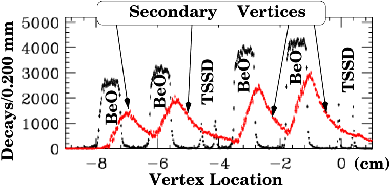
The FOCUS target region layout is schematically displayed in Fig. 1 and reconstructed vertices from charm are shown in Fig. 2. Each of the four BeO target segments is 3.0 cm square and 6.75 mm long. A 1.0 cm decay region follows each target segment. Two sets of TSSD plane doublets are located behind the second BeO target and behind the most downstream BeO target. The transverse size of the BeO target segments was chosen to match the photon beam profile. The TSSD planes are followed by a scintillator (TR1) used for triggering, four stations of Silicon Strip Detectors (SSD’s) with each station consisting of three silicon microvertex planes, and a second scintillator, (TR2). By demanding a hit in the TR1 scintillator we attempt to select interactions that occurred in the target region. A coincidence hit in TR2 reduces the number of spurious noise hits in TR1. The main vertex tracking is accomplished in the SSD’s and is described in detail in reference 3.

The components of the Target Silicon Strip Detector consist of 4, 25 micron pitch, 300 micron thick planes of silicon microstrip detector and the electronics necessary to amplify, digitize, and store the information. In Section 2 we describe the physical layout of a Target Silicon Strip plane and how the planes and target segments were mounted. In Section 3 we describe the readout electronics. In Section 4 we discuss how the hit information in the TSSD’s is matched up with the tracking information from the downstream SSD planes. In Section 5 we describe the performance of the TSSD. In section 6 we detail the use of the detector as a target rather than as an active detector.
2 Physical Description of the TSSD’s
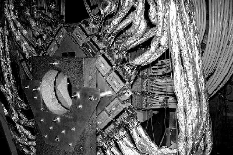
Each target silicon wafer of 2048 channels has an active area of 5 cm square. The silicon wafer is wire-bonded onto a 15 cm square, 1 mm thick quartz plate. The central 1024 channels of the silicon wafer are fanned out on the quartz plate and wire-bonded to two flexible ribbons made of very thin circuit board material. The outer 1024 (512 on a side) channels are tied together and grounded making the effective active area of each plane 2.5 cm 5 cm. The outer edge of each flexible ribbon is attached to a 132 pin Connei connector. A front and side view of a single plane is shown in Fig. 3. The planes were fabricated by MICRON SEMICONDUCTOR Limited [4] in England and were adapted from a WA85 Chip design. In order to provide greater rigidity and to allow for alignment the quartz plate is mounted onto a G-10 frame. Finally, two G-10 frames from a doublet are mounted onto a holding fixture. The holding fixture is held by bushings on low carbon steel rods which are fixed to a granite mounting. The segmented targets and the two doublets are supported by the steel rods. Precise location along the beam direction is performed using spacers on the steel rods. Finally, the planes and support structures were mounted inside a Faraday shielded, temperature controlled hut.

The two planes in each doublet are aligned at 45 degrees to the horizontal. Each plane has a coordinate in the same view as one of the views in the external SSD silicon array. The ribbons from each doublet of detectors are attached to an aluminum housing which has a separate connection to the granite support. The aluminum housing holds the individual Connei connectors and supports the front-end electronics. The advantage of this arrangement is that the front-end electronics support is disconnected from the individual silicon plane support and allows for the removal of the pre-amplifiers without damaging the wafer alignment.
We purchased five planes from MICRON SEMICONDUCTOR Limited in order to have one spare plane. All planes had a typical strip breakdown voltage in excess of 100 V. Other electrical properties for the five planes are presented in Table 1. We operated the planes with higher bias voltages (over-depletion) than the factory specified full depletion voltage listed in Table 1.
| Plane # | Thickness | Depletion | Resistance | Leakage | Leakage Current |
|---|---|---|---|---|---|
| (m) | Voltage | Between Strips | Current | at Dep. + 20 V | |
| 1 | 303 | 10.0 | 3 M | 10nA | 20 nA |
| 2 | 301 | 10.8 | 5 M | 9nA | 17 nA |
| 3 | 287 | 19.5 | 13 M | 4nA | 6 nA |
| 4 | 303 | 25.0 | 20 M | 9nA | 13 nA |
| (spare) | 291 | 20.1 | 40 M | 2nA | 5 nA |
3 Readout Electronics of the TSSD’s
The signals from each of the individual silicon strips are fed through Connei connectors into MSP1 pre-amplifiers [5]. The amplifiers are mounted on the aluminum support housing as shown in Fig. 4. The MSP1 pre-amplifiers have an intrinsic 20 ns rise time and about a 100 ns wide response to a 7 ns wide square pulse and have a good noise figure even in the presence of a high input capacitance (50 pF).222Both the added capacitance of a detector and resistance in the readout serve to increase the noise coming from a pre-amplifier.
The differential output signals from each group of MSP1’s are sent over 40 ft. long twisted pair cables that are bundled together and shielded with aluminum foil and clear packing tape. These bundles are then split into groups of 64 channels and read into electronics boards (AMP/DIG) that amplify and digitize the analog signals coming from the MSP1’s.
In the AMP/DIG boards, the signals pass through a 1:1 transformer to enhance isolation from the upstream electronics, and then are amplified by a factor of 50 using an AD8002 amplifier. The charge is integrated using an OPA660 diamond transistor as a non-feedback ns-integrator [6] to produce a voltage level for the CDX1172AM FADC chip (see Fig. 5). This voltage is sampled every 54 ns (3 accelerator buckets) and stored in a buffer memory. The RC decay time for the signal was chosen to be about 800 ns to lessen the variation of signal size for the 3 accelerator buckets covered by each sample.

When the experimental trigger fires, two signals in the buffer memory, one in–time and one 3 samples () early, are fed into an arithmetic logic unit (ALU). The earlier sample is subtracted from the in–time sample.333The baseline subtraction helps reject low frequency common-mode noise as well as reduce the effects of pile-up. If the difference exceeds the threshold stored in the ALU for that channel, the FADC information is given a channel address and stored in an output buffer. Output buffers are read out sequentially across a crate of AMP/DIG boards.
The AMP/DIG boards are organized so that each silicon plane can be read out by one crate of electronics. Each crate holds 16 9U280 mm VME boards. Constants for each board are downloaded from a CAMAC controller board specially designed to both control a crate of AMP/DIG boards and organize the information from a crate into an event record. Each event record consists of 16 bit data words, a crate identification word, and a word count. The event records from all 4 crates are transmitted from the experimental hall to the counting house at ECL levels on a single twisted flat cable. Typically, all 4 crates are read out in less than . An average event record for a target silicon plane due to a charm containing event consists of about 6 channels of electronics noise which exceeds threshold, an additional 7 channels due to pair contamination, and 14 channels due to the particles created from the charm.
The profile of hits from regular photon data is presented in Fig. 6. The number of missing and inefficient channels is of order 1-2%. Due to charge sharing, a missing channel does not necessarily translate to a loss in efficiency but rather a loss in resolution.

4 Hit Reconstruction
To incorporate the TSSD’s in the track reconstruction, we refit existing SSD tracks in a staged process. The information from the closest (most downstream) planes of the TSSD is used first. Once refit with any available information from the downstream target silicon planes, the tracks are then extrapolated to the most upstream planes and refit again. All three categories of tracks, the original SSD track, the tracks refit using the downstream TSSD information (if any), and the tracks refit using information from all TSSD planes (if any) are saved for later vertex determination. This approach allows us to include multiple coulomb scattering effects in a natural way, use the well tested SSD tracking algorithm in a seamless way, and find the best solution for the refit track at a point nearest the decay and/or production vertex.
To begin the process, the SSD tracks are first refit taking into account multiple coulomb scattering in such a manner as to find the best fit for tracks entering the SSD system.444 SSD Tracks are originally fit to optimize momentum determination, i.e. to find the best parameters for tracks leaving the SSD system.
The refit SSD tracks are extrapolated to the two most downstream target silicon planes and a three sigma search radius (about 1-2 strips typically) is identified to search for hits. The search is not allowed to extend for more than strips.
The closest non-zero (zero count ADC hits are hits that just exceed the baseline subtraction) ADC hit to an extrapolation is used as a seed to determine the number of adjacent strips that fired for the extrapolated SSD track. Once the hits are determined, a simple linear weighting between the seed hit and the adjacent hit with the largest signal is used to determine the centroid. If more than 2 hits are found, none of the hits are used in the refit, although the number of hits, the summed ADC information, and the centroid are saved. The ADC pulse height distribution for the hits found during the refit to the extrapolated SSD tracks is plotted in Fig. 7. A minimum ionizing peak is clearly observed in all planes.
To further reduce confusion the extrapolations of other SSD tracks are checked to see if there is overlap with the SSD track used to find the seed hit. No hits are allowed to be shared in the most upstream planes, but single hits in each downstream plane are allowed to be shared with another SSD track. The number of ADC hits used, and the number of overlapping SSD track extrapolations are used to determine the resolution error used in the refit.
At the end of this refit process, we use the SSD tracks and the E687 free form vertexing method [1] to determine the most likely location of the production vertex. If this vertex occurs upstream of one or both of the TSSD doublets, SSD tracks are replaced with tracks refit using the TSSD. Finally, the vertex location is used to calculate the amount of multiple coulomb scattering to include in the analysis of the event. Further refinements are possible, such as for neutral kaons that decay relatively far from the production vertex, but seldom necessary for charm reconstruction.

5 TSSD Performance
The FOCUS experiment took data during the 1996-1997 fixed target run at Fermilab from September 1996 to September 1997. The TSSD was installed in the middle of data taking during the holiday (Dec.–Jan.) shutdown of the Fermilab Tevatron. The information from the TSSD is present for about of the FOCUS data. For a short period (less than of the data containing TSSD information) after the installation, plane number 1 had readout problems that resulted in a loss of resolution and some efficiency for this plane. Otherwise, the TSSD performed consistently at high efficiency for the duration of its use. The reconstructed data, as well as the simulation of the TSSD, have been thoroughly tested and utilized in all published FOCUS physics analyses to date [7, 8, 9, 10, 11, 12, 13, 14]. With the additional information from the TSSD we significantly improved tracking resolution in the target region of the FOCUS spectrometer. The improvement is demonstrated in several tests using a representative subsample of the data.
In Fig. 8 we show the normalized transverse impact parameters in two views and for two momentum regions. Vertices with three or more tracks are refit after removing one of the tracks. This removed track is projected back to the reconstructed vertex and the transverse miss distance between the track and the vertex determined and normalized using the computed error for the miss. In order to show the improvement in resolution using the TSSD, the same error estimate is used for the case with and without the TSSD included in the tracking information. It is clear that using the TSSD information improves the position resolution.

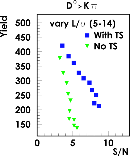
In Fig. 9 we present a plot of the charm yield for the decay using the SSD system alone and then in conjunction with the TSSD system. By making an exponential fit to drop off in yield as a function of detachment we find that we have improved lifetime resolution by . It is obvious that the charm decays have a better signal/noise ratio with higher yields for the same significance of separation.
In Fig. 10 we present a background subtracted plot of the proper time resolution and the evolution for the decay using a representative subset of the data from different running periods of the FOCUS experiment. During the running without the TSSD planes installed, the Be0 targets were moved about 1 cm closer to the SSD system. In addition to compensating for the shift of the targets away from the SSD, using the target silicon information significantly enhances the proper time resolution.

We have developed software to reconstruct long lived mesons tracks using the charm production vertex and information from the target silicon planes. In Fig. 11 we present two mass distributions of where the primary and secondary vertex information indicated that the passed through one of the Target Silicon doublets. It is evident that the signal to noise is substantially improved when confirming TSSD hits are found.

Tracks from candidates have also been reconstructed using just the information in the silicon and a single track from the decay vertex. Such a technique could be used for determining the direction for a form factor analysis of the decay . In this instance, the decays are used again to test the technique. Briefly, putative D tracks are formed using the primary vertex and target silicon hits. The D track with the highest confidence level to form a vertex with the single track from the decay vertex is retained and refit using adjacent hits (if any) in the target silicon. In Fig. 12 we show that the resolution of the D direction with this technique is comparable to a more traditional approach using the vector connecting a fully reconstructed decay vertex to the primary vertex. Since the resolutions of the two methods are highly correlated, it should be possible to make improvements, such as a better determination of the primary vertex (see Section 6 below), that benefit both techniques.

6 Target Silicon Planes as Target Elements
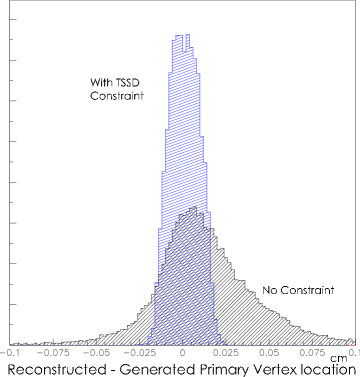
One way to improve both the direction resolution of a partially reconstructed charm decay, and the lifetime resolution for a fully reconstructed charm decay, is to improve the resolution of the primary vertex. Since two hadrons containing charm are created at the primary vertex, tracks associated with a partially reconstructed decay are sometimes included in the reconstruction of the primary vertex. Due to the finite lifetime of the charm hadrons involved, the primary vertex tends to be reconstructed downstream of its true location. One way to reduce this bias is to use a very thin target and constrain the primary vertex to be included in the target material during reconstruction. Using a full simulation of the E831 spectrometer, we have studied the improvement possible if one uses the target silicon planes as passive targets rather than a detector. In Fig. 13 we show the results of the technique. In our simulation, we find that the pull in the primary vertex location is reduced and the lifetime resolution substantially improved when we employ this technique.

7 Summary and Conclusions
We have briefly described one of the first silicon strip systems to be used inside of an experimental target. The use of the system significantly improved our lifetime and vertex resolution. We believe that our experience will prove useful to future experiments. One can imagine, for instance, a future fixed target charm experiment employing many silicon (or active diamond) planes in the target region to take advantage of the techniques presented in this paper.
Acknowledgments
We wish to acknowledge the assistance of the staffs of Fermi National Accelerator Laboratory, the INFN of Italy, and the physics departments of the collaborating institutions. This research was supported in part by the U. S. National Science Foundation, the U. S. Department of Energy, the Italian Istituto Nazionale di Fisica Nucleare and Ministero dell’Università e della Ricerca Scientifica e Tecnologica, the Brazilian Conselho Nacional de Desenvolvimento Científico e Tecnológico, CONACyT-México, the Korean Ministry of Education, and the Korean Science and Engineering Foundation.
References
- [1] E687 Collaboration, P.L. Frabetti et al., Nucl. Instrum. Methods A 320, 519 (1992).
- [2] E687 Collaboration, P.L. Frabetti et al., Nucl. Instrum. Methods A 329, 62 (1993).
- [3] G. Bellini et al., Nucl. Instrum. Methods A 252, 366 (1986).
- [4] MICRON SEMICONDUCTOR Limited, 1 Royal Buildings, Marlborough Road, Churchill Industrial Estate, Lancing, Sussex BN15 8UN, England.
- [5] J.P. Avondo et al., Nucl. Instrum. Methods A 241, 107 (1985).
- [6] The Burr-Brown Corporation, Burr-Brown Applications Handbook, p. 257 (1994).
- [7] FOCUS Collaboration, J. M. Link et al., “A high statistics measurement of the lifetime,” Accepted by Phys. Rev. Lett.
- [8] FOCUS Collaboration, J. M. Link et al., Phys. Lett. B 525, 205 (2002).
- [9] FOCUS Collaboration, J. M. Link et al., Phys. Lett. B 523, 53 (2001)
- [10] FOCUS Collaboration, J. M. Link et al., Phys. Rev. Lett. 88, 041602 (2002)
- [11] FOCUS Collaboration, J. M. Link et al., Phys. Rev. Lett. 87, 162001 (2001)
- [12] FOCUS Collaboration, J. M. Link et al., Phys. Lett. B 512, 277 (2001)
- [13] FOCUS Collaboration, J. M. Link et al., Phys. Rev. Lett. 86, 2955 (2001)
- [14] FOCUS Collaboration, J. M. Link et al., Phys. Lett. B 491, 232 (2000) [Erratum-ibid. B 495, 443 (2000)]